

SANYO LM8562 Datasheet
Ordering number: EN 2658A
PMOS LSI
LM8562
Digital Alarm Clock
Overview
The LM8562 is a digital clock-use LSI having features such as
easy setting, two alarms. Since the LM8562 is designed to be
able to direct drive an LED panel of duplex type, the package
in which the LM8562 is placed is a 28-pin shrink DIP with a
small mounting area.
Features
(1) Duplex LED display (LM8560-use LED panel usable)
(2) Two alarms on chip (600Hz, 1200 Hz)
(3) Up, down/fast, slow time setting available (easy setting)
(4) 12/24-hour mode, 50/60 Hz selectable (provided that it is
impossible to select the combination of 24-hour mode and
60 Hz)
(5) On-chip CR oscillator for backup use at the time of power
failure
(6) Power failure indicator
(7) 59-minute alarm/sleep timer
(8) 6-minute snooze function
(9) Radio output function
(10) P-channel ED MOS
(11) Pin 28 dual-in-line shrink package
(12) Wide operating voltage/operating temperature range
V
= –14 to –8 V / –20 to +70°C
DD
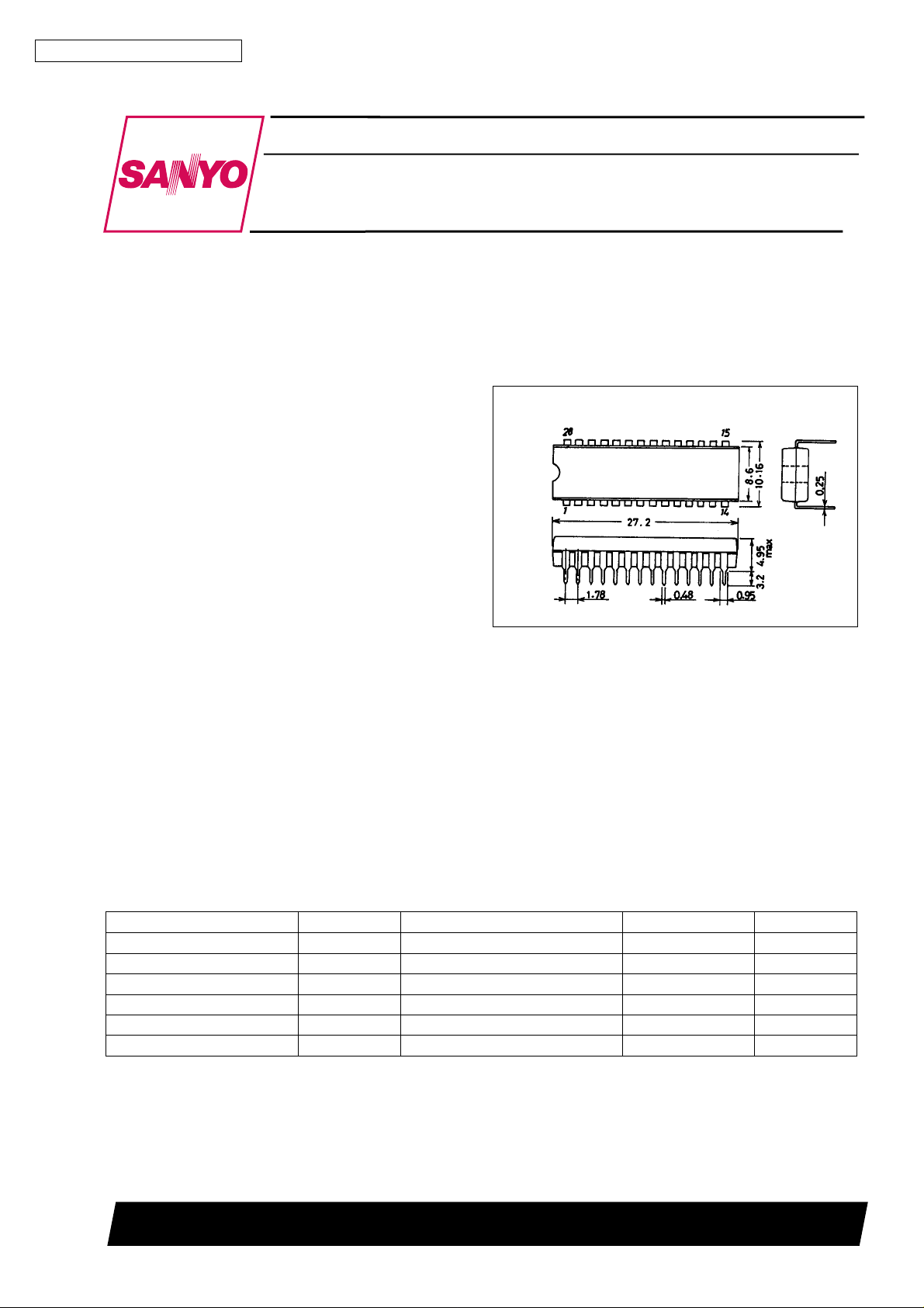
Package Dimensions
unit : mm
3029A-DIP28S
[LM8562]
SANYO : DIP28S
Specifications
Absolute Maximum Ratings at Ta = 25°C, VSS=0V
Parameter Symbol Conditions Ratings Unit
Supply voltage V
Input voltage V
Output voltage V
Allowable power dissipation Pd max Ta = 70°C 0.7 W
Operating temperature Topr –20 to +70 °C
Storage temperature Tstg –55 to +125 °C
max –17.0 to +0.3 V
DD
IN
OUT
–17.0 to +0.3 V
–17.0 to +0.3 V
SANYO Electric Co.,Ltd. Semiconductor Bussiness Headquarters
TOKYO OFFICE Tokyo Bldg., 1-10, 1 Chome, Ueno, Taito-ku, TOKYO, 110 JAPAN
D2897HA (II)/6209TA No.2658-1/7
LM8562
Allowable Operating Conditions at Ta = –20 to +70°C, VSS=0V
Parameter Symbol Conditions min typ max Unit
Supply voltage V
Standby voltage V
Input high-level voltage V
Input low-level voltage V
Input high-level voltage V
Input low-level voltage V
Input high-level voltage V
Input mid-level voltage V
Input low-level voltage V
Input high-level voltage V
Input low-level voltage V
DD
ST
1 50/60 Hz INPUT pin VSS–1 V
IH
1 VDD+2 V
IL
2 CR OSC pin VSS–1 V
IH
2V
IL
3 3-level input pins VSS– 0.7 V
IH
IM
3V
IL
4 Input pins other than the above VSS–2 V
IH
4V
IL
Input level hold time tH 10 ms
Input chattering time tC 10 ms
Electrical Characteristics atTa=25±2°C, VSS=0V,VDD= –12 V
Parameter Symbol Conditions min typ max Unit
Output high-level current I
Output OFF-state leakage current I
Output high-level current I
Output OFF-state leakage current I
Output high-level current I
Output OFF-state leakage current I
OH
OF
OH
OF
OH
OF
Operating frequency fop 50/60 Hz INPUT pin DC 2000 Hz
Input high-level current I
Input low-level current I
Input high-level current I
Input low-level current I
Input high-level current I
Input low-level current I
Pull-down resistance R
Pull-up resistance R
Operating current I
Power failure detect circuit V
IH
IL
IH
IL
IH
IL
PD
PU
DD
BU
OSC stability f
OSC accuracy f
OSC frequency f
OSC
Note 1 : The allowable segment current drain is 78 mA max. for AM & 10’SHR ag & de and 39 mA max. for other than AM &
10’SHR ag & de in the range of power dissipation 700 mW.
AM & 10’SHR ag & de pin,
1
V
OUT=VSS
1V
OUT=VDD
Segment output pins other than the
2
above, V
2V
OUT=VDD
ALM-1, ALM-2, RADIO OUTPUT pin,
3
V
OUT=VSS
3V
OUT=VDD
1VIH=V
1VIL=V
2 CR OSC pin, VIH=V
2VIL=V
3 3-level input pins, VIH=V
3VIL=V
3-level input pins, VIN= 1/2 V
VIN= 1/2V
– 2.0 V
OUT=VSS
– 2.0 V
SS
DD
DD
DD
DD
– 2.0 V
SS
SS
DD
Output : No load 2 8 15 mA
VDD=–9V±10% –10 10 %
S
VDD= –9 V –10 10 %
A
R = 180 kΩ, C = 3300 pF 2400 Hz
–14 –8 V
–7.5 V
V
SS
V
SS
+2 V
DD
SS
V
1/2 VDD– 1 1/2 VDD+1 V
DD
VDD+1 V
SS
+2 V
DD
V
32 (Note1) mA
20 µA
16 (Note1) mA
20 µA
2mA
10 µA
10 µA
–10 µA
10 µA
60 µA
20 120 µA
–120 –20 µA
1.0 MΩ
0.8 MΩ
–7.5 –5.0 V
No.2658-2/7
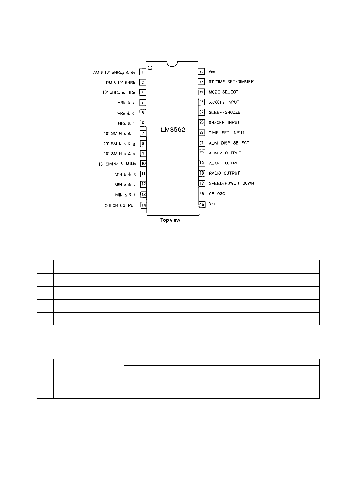
Pin Assignment
LM8562
Pin Functions
1. 3-Level Input Pins
No. Pin Name
17 SPEED/POWER DOWN Test mode Normal Power-down mode
21 ALM-DISP SELECT Alarm 2 display & setting NOP Alarm 1 display & setting
22 TIME SET INPUT Slow-down (AC = fast-down) NOP Slow-up (AC = fast-up)
23 ON/OFF INPUT ON NOP OFF
24 SLEEP/SNOOZE Sleep display & sleep-in NOP Second display & snooze-in
26 MODE SELECT 24-hour mode, 50 Hz 12-hour mode, 50 Hz 12-hour mode, 60 Hz
27 RT-TIME SET/DIMMER Time setting inhibit
Dimmer display
V
SS
NOP : No operation
AC : Pulse input
2. Input/Output Pins
No. Pin Name
18 RADIO OUTPUT — When not used
19 ALM-1 OUTPUT — Alarm1 OFF
20 ALM-2 OUTPUT — Alarm2 OFF
16 CR OSC 1-pin OSC circuit
V
SS
3. Input Pins
No.25 50/60 Hz INPUT = 50 Hz or 60 Hz clock signal input
No.15, 28 V
SS,VDD
= Power supply pin
Input Level
OPEN V
Timer setting inhibit
Normal display
Input Level
DD
Time setting enable
Normal display
V
DD
No.2658-3/7
 Loading...