

SANYO LM7001JM, LM7001J Datasheet
Ordering number : EN5262
D3095HA (OT) No. 5262-1/8
Features
• The LM7001J and LM7001JM are PLL frequency
synthesizer LSIs for tuners, making it possible to make
up high-performance AM/FM tuners easily.
• These LSIs are software compatible with the LM7000,
but do not include an IF calculation circuit.
• The FM VCO circuit includes a high-speed
programmable divider that can divide directly.
• Seven reference frequencies: 1, 5, 9, 10, 25, 50, and
100 kHz
• Band-switching outputs (3 bits)
• Controller clock output (400 kHz)
• Clock time base output (8 Hz)
• Serial input circuit for data input (using the CE, CL, and
DATA pins)
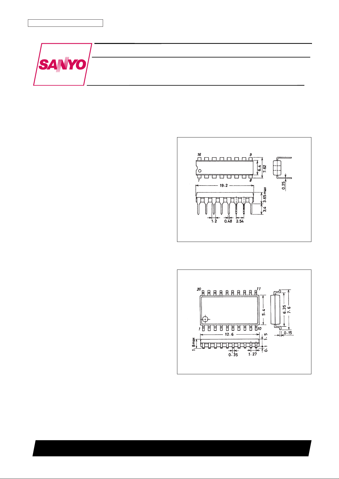
Package Dimensions
unit: mm
3006B-DIP16
unit: mm
3036B-MFP20
SANYO: DIP16
[LM7001J]
SANYO: MFP20
[LM7001JM]
LM7001J, 7001JM
SANYO Electric Co.,Ltd. Semiconductor Bussiness Headquarters
TOKYO OFFICE Tokyo Bldg., 1-10, 1 Chome, Ueno, Taito-ku, TOKYO, 110-8534 JAPAN
Direct PLL Frequency Synthesizers
for Electronic Tuning
NMOS LSI
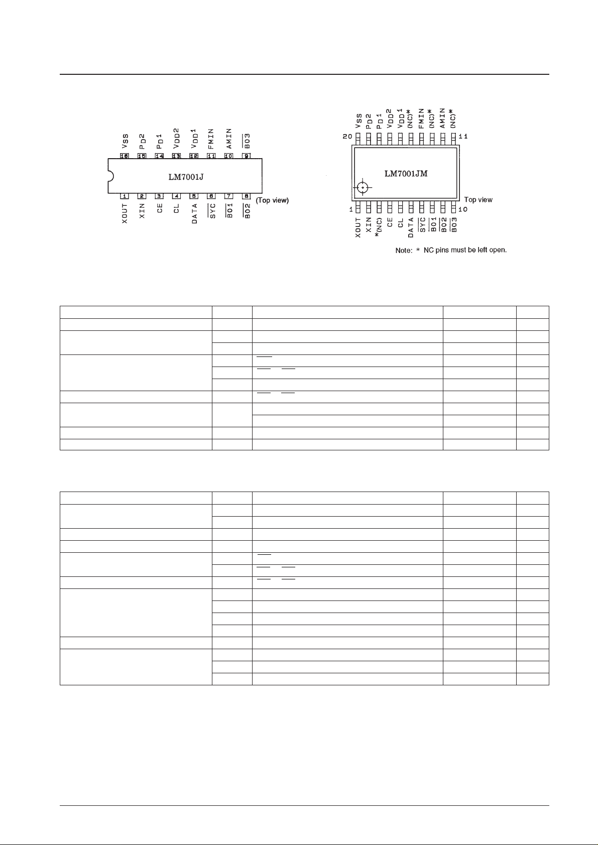
Pin Assignments
Specifications
Absolute Maximum Ratings at Ta = 25°C, VSS= 0 V
Allowable Operating Ranges at Ta = –40 to +85°C, VSS= 0 V
Note: 1. f
ref
= 25, 50, or 100 kHz
2. f
ref
= Reference frequencies other than those for *1.
3. “s” refers to the control bit in the serial data.
No. 5262-2/8
LM7001J, 7001JM
Parameter Symbol Conditions Ratings Unit
Maximum supply voltage V
DD
max VDD1, VDD2 –0.3 to +7.0 V
Maximum input voltage
V
IN
1 max CE, CL, DATA –0.3 to +7.0 V
V
IN
2 max Input pins other than VIN1 –0.3 to VDD+ 0.3 V
V
OUT
1 max SYC –0.3 to +7.0 V
Maximum output voltage V
OUT
2 max BO1 to BO3 –0.3 to +13 V
V
OUT
3 max Output pins other than V
OUT
1 and V
OUT
2 –0.3 to VDD+ 0.3 V
Maximum output current I
OUT
max BO1 to BO3 0 to 3.0 mA
Allowable power dissipation Pd max
Ta = 85°C: LM7001J (DIP16) 300 mW
Ta = 85°C: LM7001JM (MFP20) 180 mW
Operating temperature Topr –40 to +85 °C
Storage temperature Tstg –55 to +125 °C
Parameter Symbol Conditions Ratings Unit
Supply voltage
V
DD
1 VDD1, PLL circuit operating 4.5 to 6.5 V
V
DD
2 VDD2, crystal oscillator time base 3.5 to 6.5 V
Input high-level voltage V
IH
CE, CL, DATA 2.2 to 6.5 V
Input low-level voltage V
IL
CE, CL, DATA 0 to 0.7 V
V
OUT
1 SYC 0 to 6.5 V
Output voltage
V
OUT
2 BO1 to BO3 0 to 13 V
Output current I
OUT
BO1 to BO3, VDD= 4.5 to 6.5 V 0 to 3.0 mA
f
IN
1 XIN, sine wave, capacitor coupled 1.0 to 7.2 typ to 8.0 MHz
Input frequency
f
IN
2 FMIN, sine wave, capacitor coupled*1, s*3= 1 45 to 130 MHz
f
IN
3 FMIN, sine wave, capacitor coupled*2, s*3= 1 5 to 30 MHz
f
IN
4 AMIN, sine wave, capacitor coupled, s*3= 0 0.5 to 10 MHz
Crystal element for guaranteed oscillation Xtal XIN to XOUT, CI ≤ 30 Ω 5.0 to 7.2 typ to 8.0 MHz
V
IN
1 XIN, sine wave, capacitor coupled 0.5 to 1.5 Vrms
Input amplitude V
IN
2 FMIN, sine wave, capacitor coupled 0.1 to 1.5 Vrms
V
IN
3 AMIN, sine wave, capacitor coupled 0.1 to 1.5 Vrms
Electrical Characteristics in the Allowable Operating Ranges
Note: 1. VDD= 3.5 to 6.5 V
2. With a 7.2 MHz crystal connected between XIN and XOUT, f
IN
2 = 130 MHz, VIN2 = 100 mVrms, other input pins at VSS, output pins open.
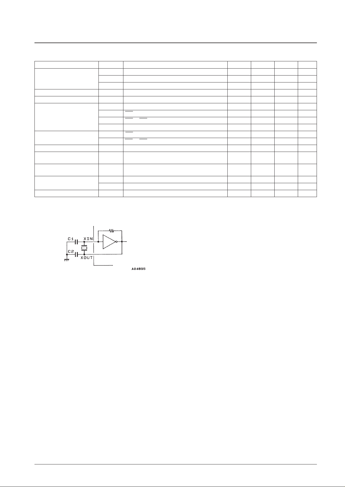
Oscillator Circuit Example
Kinseki, Ltd.
HC43/U: 2114-84521 (1): CL = 10 pF, C1 = 15 (10 to 22) pF, C2 = 15 pF
HC43/U: 2114-84521 (2): CL = 16 pF, C1 = 22 (15 to 33) pF, C2 = 33 pF
Nihon Denpa Kogyou, Ltd.
NR-18: LM-X-0701: CL = 10 pF, C1 = 15 pF, C2 = 15 pF
Since the circuit constants in the crystal oscillator circuit depend on the crystal element used and the printed circuit board
pattern, we recommend consulting with the manufacturer of the crystal element concerning this circuit.
No. 5262-3/8
LM7001J, 7001JM
Parameter Symbol Conditions min typ max Unit
R
f1
XIN 1.0 MΩ
Built-in feedback resistance R
f2
FMIN 500 kΩ
R
f3
AMIN 500 kΩ
Input high-level current I
IH
CE, CL, DATA: VIN= 6.5 V 5.0 µA
Input low-level current I
IL
CE, CL, DATA: VIN= 0 V 5.0 µA
V
OL
1 FMIN, AMIN: I
OUT
= 0.5 mA 3.5 V
V
OL
2 SYC: I
OUT
= 0.1 mA,
*1
0.02 0.3 V
Output low-level voltage
V
OL
3 BO1 to BO3: I
OUT
= 2.0 mA 1.0 V
V
OL
4 PD1, PD2: I
OUT
= 0.1 mA 0.3 V
Output off leakage current
I
OFF
1 SYC: V
OUT
= 6.5 V 5.0 µA
I
OFF
2 BO1 to BO3: V
OUT
= 13 V 3.0 µA
Output high-level voltage V
OH
PD1, PD2: I
OUT
= –0.1 mA 0.5 V
DD
V
High-level 3-state
I
OFFH
PD1, PD2: V
OUT
= V
DD
0.01 10.0 nA
off leakage current
Low-level 3-state
I
OFFL
PD1, PD2: V
OUT
= 0 V 0.01 10.0 nA
off leakage current
Current drain
I
DD
1 VDD1 + VDD2:
*2
25 40 mA
I
DD
2 VDD2: PLL block stopped 2.0 3.5 mA
Input capacitance C
IN
FMIN 1 2 3 pF
 Loading...