

SANYO LE28FV4001T-25, LE28FV4001T-20, LE28FV4001R-25, LE28FV4001M-20, LE28FV4001R-20 Datasheet
...
Ordering number : EN*5468
22897HA(OT) No. 5468-1/14
Overview
The LE28FV4001M, T, R Series are 4 MEG flash
memory products that feature a 542488-word × 8-bit
organization and 3.3 V single-voltage power supply
operation. CMOS peripheral circuits were adopted for
high speed, low power, and ease of use. The
LE28FV4001M also supports high-speed data rewriting
by providing a sector (256 bytes) erase function.
Features
• Highly reliable 2 layer polysilicon CMOS flash
EEPROM process
• Read and write operations using a 3.3 V single-voltage
power supply
• High-speed access: 200 and 250 ns
• Low power
— Operating (read): 10 mA (maximum)
— Standby: 20 µA (maximum)
• Highly reliable read write
—Number of sector write cycles: 104cycles
— Data retention: 10 years
• Address and data latches
• Sector erase function: 256 bytes per sector
• Self-timer erase/program
• Byte program time: 35 µs (maximum)
• Write complete detection function: Toggle bit/Data
poling
• Hardware and software data protection functions
• Pin assignment conforms to the JEDEC byte-wide
EEPROM standard.
• Package
SOP 32-pin (525 mil) plastic package: LE28FV4001M
TSOP 42-pin (10 × 14 mm) plastic package:LE28FV4001T
TSOP 40-pin (10× 14 mm) plastic package: LE28FV4001R
Package Dimensions
unit: mm
3205-SOP32
unit: mm
3087A-TSOP40
Preliminary
SANYO: SOP32
[LE28FV4001M. T, R]
SANYO: TSOP40 (TYPE-I)
[LE28FV4001M. T, R]
LE28FV4001M, T, R-20/25
SANYO Electric Co.,Ltd. Semiconductor Bussiness Headquarters
TOKYO OFFICE Tokyo Bldg., 1-10, 1 Chome, Ueno, Taito-ku, TOKYO, 110-8534 JAPAN
4MEG (52488 × 8 Bits) Flash Memory
CMOS LSI
These FLASH MEMORY products incorporate technology licensed from Silicon Storage Technology, Inc.
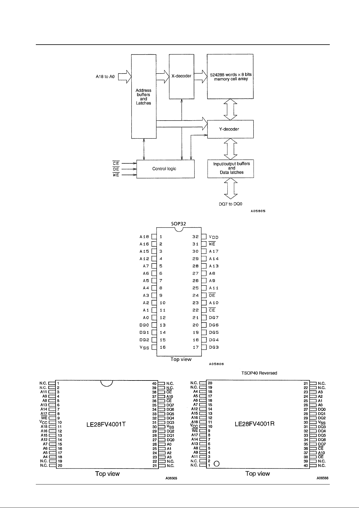
Block Diagram
Pin Assignments
No. 5468-2/14
LE28FV4001M, T, R-20/25

Pin Functions
Function Logic
Command Settings
Notes on command settings
1. X = high or low
2. The sector address is taken from A8 to A18, the sector size is 256 bytes, and A0 to A7 can be high or low during a sector erase operation.
3. The program address is taken from A0 to A18.
4. Data is displayed in hexadecimal.
5. SDP refers to the software data protect function, which uses a 7-byte read cycle sequence.
Y = Can be executed even when the software data protect function is enabled.
N = Cannot be executed when the software data protect function is enabled.
6. Figures 9 and 10 show the operation of the software data protect function using 7-byte read cycle sequences.
7. When an address of 0000 is specified, the manufacturer code, BF, is output, and when the address is 0001, the device code, 04, is output.
No. 5468-3/14
LE28FV4001M, T, R-20/25
Symbol Pin Functions
A18 to A0 Address input
Supply the memory address to these pins.
The address is latched internally during a write cycle.
These pins output data during a read cycle and input data during a write cycle.
DQ7 to DQ0 Data input and output Data is latched internally during a write cycle.
Outputs go to the high-impedance state when either OE or CE is high.
CE Chip enable
The device is active when CE is low.
When CE is high, the device becomes unselected and goes to the standby state.
OE Output enable
Makes the data output buffers active.
OE is a low-active input.
WE Write enable
Makes the write operation active.
WE is an active-low input.
V
DD
Power supply Apply 3.3 V ±0.3 V to this pin.
V
SS
Ground
N.C. No connection These pins are not connected to the chip internally.
Mode CE OE WE A18 to A0 DQ7 to DQ0
Read V
IL
V
IL
VIHA
IN
D
OUT
Write V
IL
V
IH
VILA
IN
D
IN
Standby or write inhibit V
IH
X X X High-Z
Write inhibit
X V
IL
X X High-Z/D
OUT
X X VIHX High-Z/D
OUT
A18 to A10 = VIL, A8 to A1 = VIL,
Manufacturer code (BF)
Product identification V
IL
V
IL
V
IH
A9 = 12 V, A0 = V
IL
A18 to A10 = VIL, A8 to A1 = VIL,
Device code (04)
A9 = 12 V, A0 = V
IH
Command
Request Setup command cycle Execute command cycle
SDP
cycles Operation Address Data Operation Address Data
Sector erase 2 Write X 20H Write Sector address D0H N
Byte program 2 Write X 10H Write Program address Program data N
Reset 1 Write X FFH Y
Read ID 3 Write X 90H Read (7) (7) Y
Software data unprotect 7 See Figure 9.
Software data protect 7 See Figure 10.

Product Overview
The LE28FV4001M, LE28FV4001T, and LE28FV4001R are 524288-word × 8-bit flash memory products that provide
sector erase and byte programming functions. These flash memories can be erased and programmed using a 3.3-volt
single-voltage power supply, they conform to the JEDEC standards for byte-wide memory pin assignments, and are pin
compatible with industry standard EPROM, flash EPROM, and EEPROM memories.
The maximum byte programming time for the LE28FV4001M, LE28FV4001T, and LE28FV4001R is 35 µs, and the
maximum sector erase time is 4 ms. Optimization is possible using the toggle bit and Data polling functions, which
indicate the completion of the write cycle for both programming and erase operations. These products provide both
hardware and software protection functions to protect data from being overwritten unintentionally. These products
guarantee 10,000 rewrite cycles in sector units. Data is retained for at least 10 years.
The block diagram for these products as well as the pin assignments for the 40-pin TSOP and 32-pin SOP packages are
shown on page 2. The pin functions and command settings are listed on page 3.
Device Operation
Commands are provided to access the device memory operation functions. The commands are written to a command
register with standard microprocessor write timing. Commands are written by setting WE to the low level while CE is
held low. The address is latched on the falling edge of WE or CE, whichever falls last. Data is latched on the rising edge
of WE or CE, whichever rises first. However, during the software write protect sequence, the address is latched on the
rising edge of OE or CE, whichever rises first.
Command Definition
The Command Settings section on page 3 presents a list of the commands and an overview of their functions. This
section describes those functions in detail.
To execute the LE28FV4001M, LE28FV4001T, and LE28FV4001R byte program or erase function, the software protect
function must be executed first.
1. Sector erase operation
The sector erase operation consists of a setup command and an execute command. The setup command sets the
device to a state where all the bytes within the sector can be erased electrically. A sector has 256 bytes. Since almost
all applications use erase operations that are not whole chip erase operations but rather are single sector erase
operations, this sector erase operation significantly increases the flexibility and ease-of-use of the LE28F4001 Series.
The setup command is executed by writing 20H to the command register.
An execute command (DDH) must be written to the command register to execute the sector erase operation. The
sector erase operation starts on the rising edge of WE pulse and is automatically completed by an internal timer.
Figure 6 shows the timing and waveforms for this operation.
This two-stage sequence in which a setup command and a following execute command are required guarantees that
the memory at the sector specified by the address data will not be erased accidentally.
2. Sector erase flowchart
The quick and reliable erasure of up to 256 bytes of memory can be achieved by following the sector erase flowchart
shown in Figure 1. The whole operation consists of executing two commands. A sector erase operation completes in
a maximum of 4 ms. Although the erase operation can be terminated by executing a reset operation, the sector may
not be completely erased if that reset is executed before the 4 ms time-out period elapses. The erase command can be
re-executed as many times as required before the erase completes. Excessive erasure cannot cause problems with the
LE28FV4001 Series products.
No. 5468-4/14
LE28FV4001M, T, R-20/25

3. Byte programming operation
The byte programming operation is started by writing a setup command (10H) to the command register.
Once the setup command is executed, the execute command is started by the next WE pulse transition. Figure 7
shows the timing waveforms for this operation. The address and the data are latched internally on the falling edge
and rising edge of the WE pulse, respectively. The WE rising edge also corresponds to the start of the programming
operation. The programming operation is automatically completed under internal timing control. Figures 2 and 7
show the programming characteristics and waveforms.
As mentioned previously, this two-stage sequence in which a setup command and a following execute operation, are
required guarantees that memory cells will not be programmed accidentally.
4. Byte programming flowchart
Data is stored into the device (i.e., the device is programmed) by the byte programming flowchart shown in Figure 2.
The byte programming command sets up the byte for writing. The address is latched on the falling edge of WE or
CE, whichever falls last. The data is latched on the rising edge of WE or CE, whichever rises first, and the
programming operation starts. The application can detect the completion of the write by Data polling or by using the
toggle bit.
5. Reset operation
The reset command is a procedure for safely terminating an erase or programming command sequences. Writing
FFH to the command register after issuing an erase or programming setup command will safely cancel that operation.
The contents of memory will not be changed. The device goes to read mode after executing a reset command. The
reset command cannot activate the software data protect function. Figure 8 shows the timing wavefroms.
6. Read operation
A read operation is performed by setting CE and OE, and then WE to read mode. Figure 3 shows the read mode
timing waveforms, and the read mode conditions are shown as “function logic”. A read cycle from the host searches
for the memory array data. The device remains in the read state until another command is written to the command
register.
As a default, the device will be in read mode in the write protect state from the time power is first applied until a
command is written to the command register. The unprotect sequence must be executed to perform a write operation
(erase or programming).
The read operation is controlled by CE and OE, and both must be set to the logic low level to activate the read
function. When CE is at the logic high level, the chip is in the unselected state and only draws the standby current.
OE controls the output pins. The device output pins will be in the high-impedance state if either CE or OE is at the
logic high level.
7. Read ID operation
The read ID operation consists of a single command, 90H. A read operation from address 0000H will then return the
manufacturer code, BFH and a read operation from address 0001H will return the device code, 04H. This operation
is terminated by writing any other valid command to the command register.
Protecting Data from Unintentional Writes
To protect the accumulated stored data that the user intends to be nonvolatile, the LE28FV4001 Series products provide
both hardware and software functions to prevent unintentional writes when power is applied or cut off.
1. Hardware data protection
The LE28FV4001 Series products incorporate a hardware data function that prevents unintentional writes.
• Write inhibit mode: Write operations are disabled if either OE is at the low logic level, CE is at the high logic level,
or WE is at the high logic level.
• Noise and glitch protection: WE pulses shorter than 15 ns will not execute a write operation.
• The LE28FV4001 Series products were designed to hold unintentional writes to a minimum by setting the device
to read mode as the default when power is first applied.
No. 5468-5/14
LE28FV4001M, T, R-20/25
 Loading...