

Page 1
FILE NO.
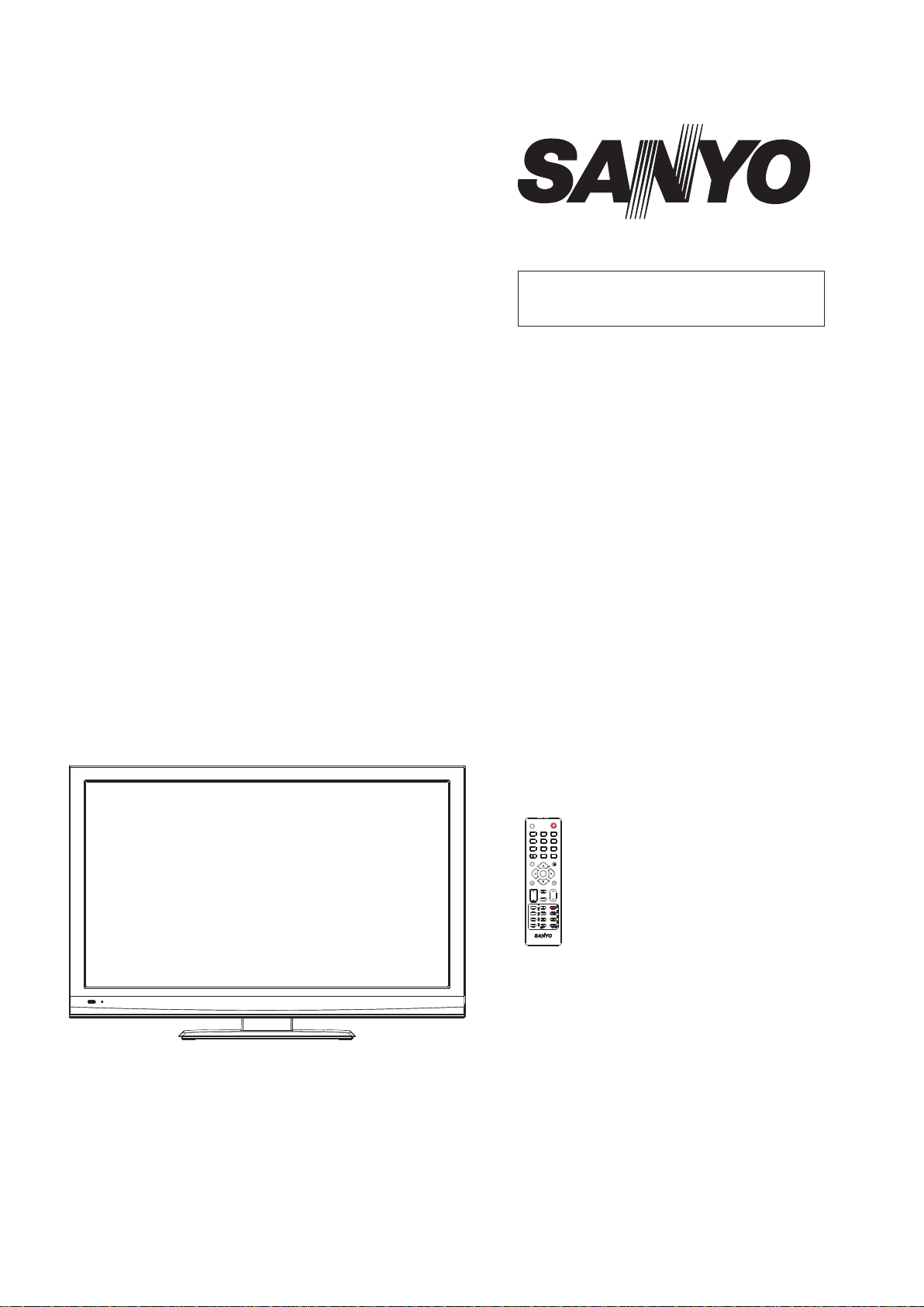
SERVICE MANUAL
LED-LCD TV
LCE-32R77
PRODUCT CODE No.
PRODUCT CODE No.
1 682 351 96: PAL/SECAM
-B/G, D/K, I
NTSC(AV)
INPUT
3
2
1
6
5
4
8
9
7
FREEZE
0
SLEEP
DISPLAY
ENTER
EXIT
MENU
MUTE
VOL CH
FAVORITE
TTX
FUNCTION
ZOOM
MIX
AUTO/STEREO
INDEX
PICTURE
SUBTITLE
SOUND
TEXT/USB
RC-1310-0A
REFERENCE No.:SM0915230
Page 2

CONTENTS
Safety precautions………………………………………………………………………..…
Alignment instructions …………………………….…….…………………………………
Software upgrade instructions ..................................................................................
Working principle analysis……………………………….………….…………...............
Block diagram…………………………………..………………………………….…………
IC block diagram………………………………………………………………………..……
Wiring diagram …………………………………………………………………………….
Troubleshooting flow chart ………………………………………………………………..……
Schematic diagram…………………………………………………………………………
APPENDIX-A: Assembly list
APPENDIX-B: Exploded View
Assembling the Stand
WALL MOUNTING INSTRUCTIONS
3
5
11
16
17
18
32
33
36
Page 3

Attention: This service manual is only for service personnel to take reference with. Before
servicing please read the following points carefully.
Safety precautions
1. Instructions
Be sure to switch off the power supply before replacing or welding any components or
inserting/plugging in connection wire. Anti static measures must be taken (throughout the entire
production process!):
a) Do not touch here and there by hand at will;
b) Be sure to use anti static electric iron;
c) It’s necessary for the welder to wear anti static gloves.
Please refer to the part list before replacing components that have special safety requirements.
Do not replace with different components with different specs and type at will.
2. LCD servicing precautions
2.1 Screens are different from one model to another and therefore not interchangeable. Be sure to
use the screen of the original model for replacement.
2.2 The operation voltage of LCD screen is 700-825V. Be sure to take proper measures in
protecting yourself and the machine when testing the system in the course of normal operation or
right after the power is switched off. Please do not touch the circuit or the metal part of the module
that is in operation mode. Relevant operation is possible only one minute after the power is
switched off.
2.3 Do not use any adapter that is not identical with the TV set. Otherwise it will cause fire or
damage to the set.
2.4 Never operate the set or do any installation work in bad environment such as wet bathroom,
laundry, kitchen, or nearby fire source, heating equipment and devices or exposure to sunlight etc.
Otherwise bad effect will result.
2.5 If any foreign substance such as water, liquid, metal slices or other matters happens to fall into
the module, be sure to cut the power off immediately and do not move anything on the module lest
it should cause fire or electric shock due to contact with the high voltage or short circuit.
2.6 Should there be smoke, abnormal smell or sound from the module, please shut the power off
at once. Likewise, if the screen is not working after the power is on or in the course of operation,
the power must be cut off immediately and no more operation is allowed under the same
condition.
2.7 Do not pull out or plug in the connection wire when the module is in operation or just after the
power is off because in this case relatively high voltage still remains in the capacitor of the driving
circuit. Please wait at least one minute before the pulling out or plugging in the connection wire.
2.8 When operating or installing LCD please don’t subject the LCD components to bending,
twisting or extrusion, collision lest mishap should result.
2.9 As most of the circuitry in LCD TV set is composed of CMOS integrated circuits, it’s necessary
to pay attention to anti statics. Before servicing LCD TV make sure to take anti static measure and
ensure full grounding for all the parts that have to be grounded.
2.10 There are lots of connection wires between parts behind the LCD screen. When servicing or
moving the set please take care not to touch or scratch them. Once they are damaged the screen
Page 4
would be unable to work and no way to get it repaired.
If the connection wires, connections or components fixed by the thermotropic glue need to
disengage when service, please soak the thermotropic glue into the alcohol and then pull them
out in case of dagmage.
2.11 Special care must be taken in transporting or handling it. Exquisite shock vibration may lead
to breakage of screen glass or damage to driving circuit. Therefore it must be packed in a strong
case before the transportation or handling.
2.12 For the storage make sure to put it in a place where the environment can be controlled so as
to prevent the temperature and humidity from exceeding the limits as specified in the manual. For
prolonged storage, it is necessary to house it in an anti-moisture bag and put them altogether in
one place. The ambient conditions are tabulated as follows:
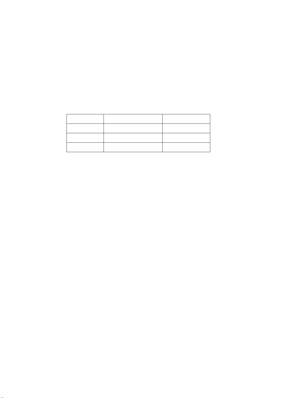
Temperature Operation range +5 ~ +35 oC
Storage range -20 ~ +60 oC
Humidity Operation range 20% ~ 80%
Storage range 10% ~ 90%
2.13 Display of a fixed picture for a long time may cause a permanent after-image on the screen,
as commonly called “ghost shadow”. The degree of the after-image varies with the maker of LCD
screen. This phenomenon doesn’t represent failure. This “ghost shadow” may remain in the
picture for a period of time (several minutes). But when operating it please avoid displaying still
picture in high brightness for a long time.
3. Installation precautions
3.1 The front panel of LCD screen is made of glass. When installing it please make sure to put it in
place.
3.2 For service or installation it’s necessary to use specified screw lest it should damage the
screen.
3.3 Be sure to take anti dust measures. Any foreign substance that happens to fall down between
the screen and the glass will affect the receiving and viewing effect
3.4 When dismantling or mounting the protective partition plate that is used for anti vibration and
insulation please take care to keep it in intactness so as to avoid hidden trouble.
3.5 Be sure to protect the cabinet from damage or scratch during service, dismantling or
mounting.
Page 5
Adjustment Instructions
1 Safety Instructions
1.1 Power supply must be cut off when replacing or welding any component or inserting / pulling out
connective lines;
1.2 Anti-electrostatic measures must be carried out during the whole producing processes!
a) Do not touch IC by hands at will;
b) Use anti-electrostatic iron;
c) Welder must wear anti-electrostatic glove;
1.3 Replacing any component with special safety requirement must refer to component list without
changing its specification and model at will.
1.4 Power supply voltage must be ~(100-240) V±10% 50 Hz.
2 Adjustment Equipments
VG-848 (YPbPr, VGA signal generator)
VG-848 (HDMI signal generator)
CA-210
3 Adjustment Processes
3.1 Power voltage test
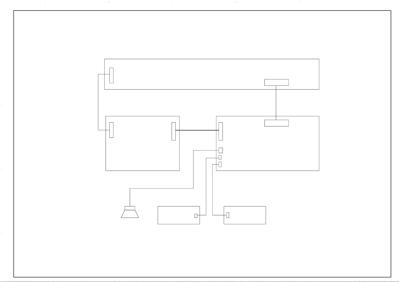
According to the wiring diagram ‘9232ME7001JL’, connect power board assembly, data
processing assembly, IR/Key board assembly correctly, supply with power, press button standby
to turn on the TV set.
3.11 Model LC-32MEXX
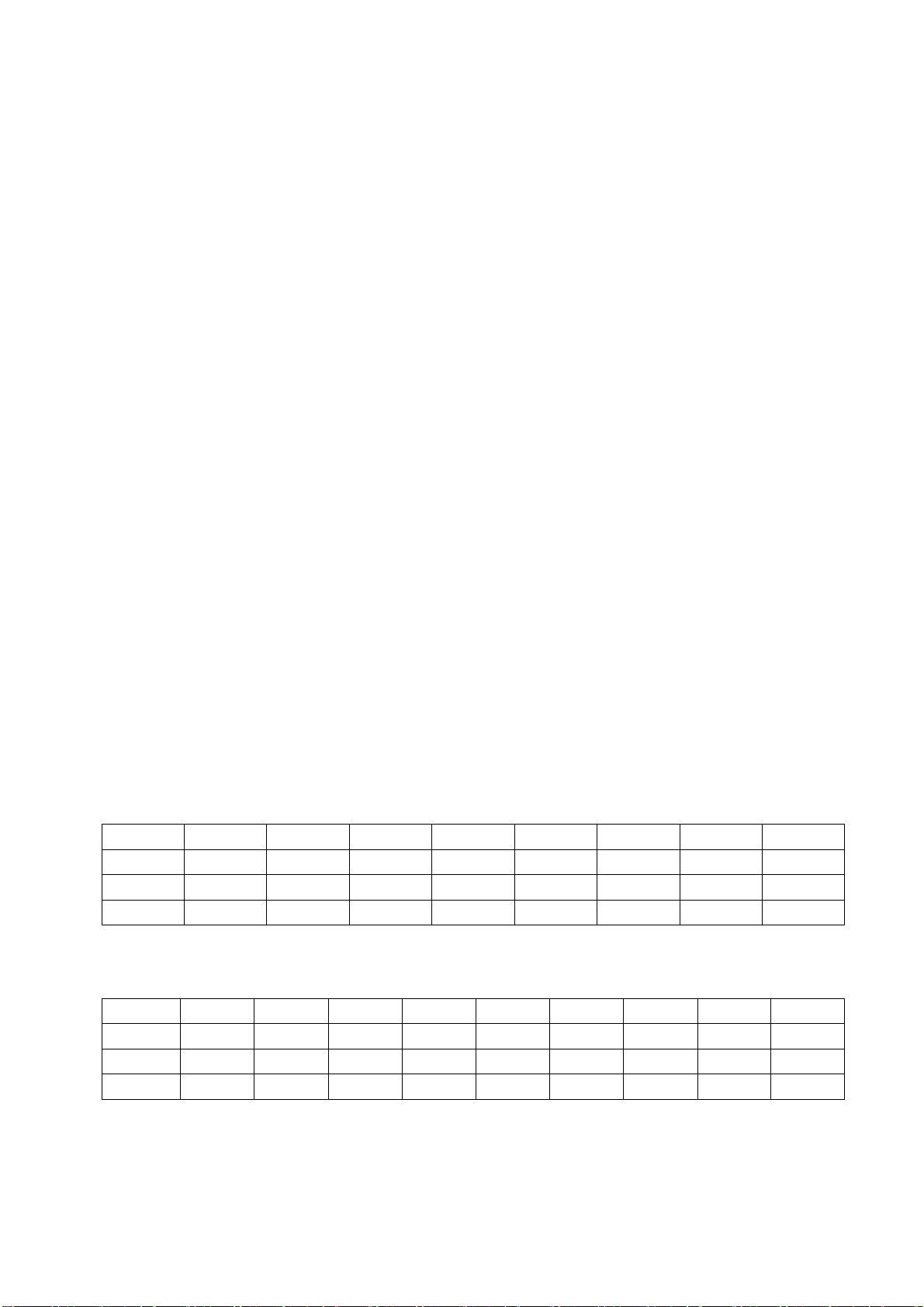
Test voltage of X301 each pin on power board in turn shown as Table 1:
Table 1 Voltage of X301 each pin
X301
Min. (V) 0 11.3 0 4.85 4.85 4.85 3.25 4.85
Typical(V) 0 12.0 0 5.00 5.00 5.00 3.30 5.00
Max. (V) 0 12.6 0 5.35 5.35 5.35 3.35 5.07
Pin 1
2、3 4、5
6 7 8 9 10
3.12 Model LE-32/42MEXX and LC-39/46/50MEXX
Test voltage of X301 each pin on power board in turn shown as Table 2:
Table 2 Voltage of X301 each pin
Pin 1、2 3、4 5、6 7、8
X301
Min. (V) 11.3 0 11.3 0 4.85 4.85 4.85 3.25 4.85
Typical(V) 12.0 0 12.0 0 5.00 5.00 5.00 3.30 5.00
Max. (V) 12.6 0 12.6 0 5.35 5.35 5.35 3.35 5.07
9 10 11 12 13
3.13 Model LE-46/55MEXX
Test voltage of X301 each pin on power board in turn shown as Table 3:
Page 6
X301
最小(V)
典型(V)
最大(V)
Pin 1、2 3、4 5、6 7、8
24.3 0 11.3 0 4.85 4.85 4.85 3.25 4.85
24.0 0 12.0 0 5.00 5.00 5.00 3.30 5.00
23.6 0 12.6 0 5.35 5.35 5.35 3.35 5.07
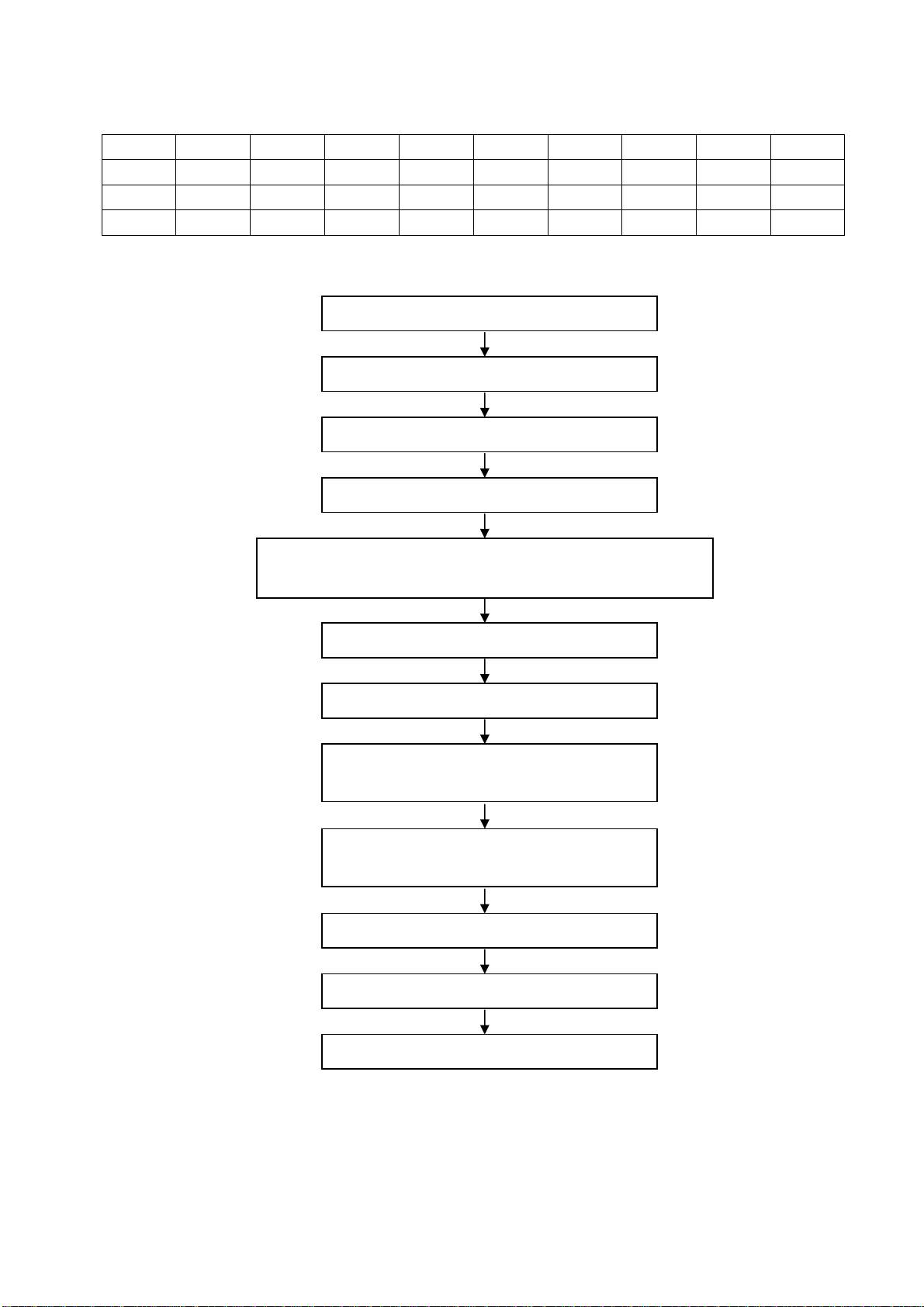
3.2 Adjustment flow as Fig. 1:
Input central signal, check TV function (omitted channel, analog
parameters control, etc. ), check earphone, speakers output.
Table 3 Voltage of X301 each pin
9 10 11 12 13
Check if DDC、FLASH has been written?
Produce data processing board on line.
General assembly and combined adjustment
White balance adjustment
Input AV signal, check relevant functions.
Input HDMI signal (mode), check YPbPr functions.
Input VGA signal, check display and all functions
(such as analog parameter), H/V center, etc..
Input HDMI signal, check display and all functions
(such as analog parameter), H/V center, etc..
Input USB signal, check relevant functions.
Default settings before shipment
Check accessory and packing
Fig. 1 Adjustment flow chart
Page 7

4 Adjustment Instructions
4.1 The unit adjustments
4.1.1 According to the wiring diagram “9232ME7001JL”, connect power/backlight board assembly,
data processing assembly, IR/Key board assembly correctly, supply with power, turn on the TV set.
Check display.
4.1.2 Factory menu instruction
a) Press key “INPUT”, press digital keys “2、5、8、0” in turn to enter into primary factory menu;
b) Press keys “” and “” to move cursor to each page of primary factory menu, then press
key “ENTER” to enter into submenu page;
c) Press keys “” and “” to move cursor upward or downward within any one page;
d) Press keys “” and “” to do adjustment when move cursor to one item;
e) Press key “MENU” to exit submenu page of factory menu sequentially;
f) Press key “EXIT” to exit factory menu in any case;
g) Factory menu item: Aging Mode to be used for aging the TV set when the option is “On”;
press any key on key board to exit aging mode during the aging process;
h) Factory menu item: Othersetting → Power on mode:
‘On’: to turn on the TV set with one step;
‘Off’: to turn on the TV set with two steps;
‘Memory’: to keep the last power-off state when power on the TV set again;
4.2 White balance adjustment
4.2.1 Before adjustment
The TV set should be working above 30 minutes to be in a stabler state before adjustment. Use
CA-210 BBY channel to adjust white balance;
a) VGA channel adjustment
Input square signal (VG848 Timing: 854 (VESA 800
×600/60 Hz), enter into user menu
Setup→VGA Setting→ AUTO to make picture display fully; then input signal (VG848 PAT: 914),
enter into factory menu page ADC ADJUST to perform AUTO ADC until the prompt “SUCCESS”
displays.
b) YPbPr channel adjustment
Input signal (VG848 Timing: 968 (480i/60 Hz),PAT: 918 (100% color bar + gray scale)) ,
enter into factory menu page ADC ADJUST to perform AUTO ADC until the prompt “SUCCESS”
displays.
c) Only Normal color temperature need adjusting for the model. Chromatic coordinates of bright
scale must be set as (△X=±5, △Y=±5), chromatic coordinates of dark scale must be set as (△X=±10,
△Y=±10). Chromatic coordinates of each model are listed as Table 4:
Table 4 Chromatic coordinates of each model
WARM NORMAL COOL
6500K(313、329) 9300K(285、293) 12000K(272、278)
Page 8
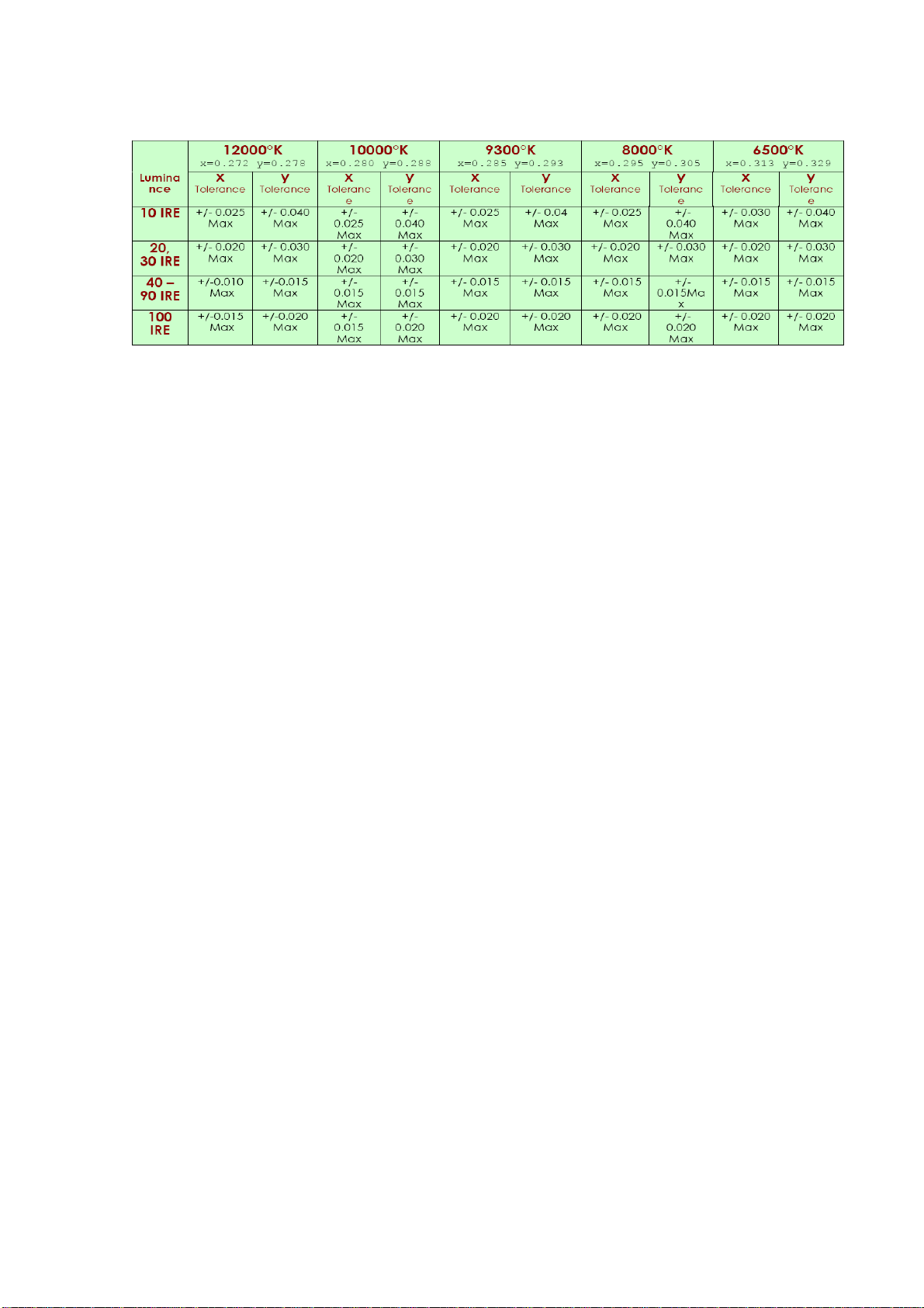
d)BBY:Insignia-Dynex TV Spec Part of chromatic coordinates are listed as Fig. 2:
Fig.2 Chromatic coordinates of white balance
4.2.2 Four groups of white balance adjustments
4.2.2.1 DVI channel adjustment (HDMI,USB channel with the same adjustment method of this one)
Input signal (VG848 Timing: 854,PAT: 921 (16-gray-step)), enter into factory menu page Color
Temp, fix item G-GAIN, adjust items R-GAIN、B-GAIN to set chromatic coordinates of the reversed
th
scale as the date of NORMAL; fix item G-OFFSET, adjust items R-OFFSET、B-OFFSET to set
4
th
chromatic coordinates of the 4
scale as the date of NORMAL; adjust items R-GAIN、B-GAIN and
R-OFFSET、B-OFFSET repeatedly as above until chromatic coordinates of both gray scales are the
date of NORMAL;
Check if chromatic coordinates of WARM is (313、329), if not, adjust items R GAIN / B GAIN /
R OFF/ B OFF to be up to the requirements and then save the date.
Check if chromatic coordinates of COOL is (272、278), if not, adjust items R GAIN / B GAIN /
R OFF/ B OFF to be up to the requirements and then save the date.
4.2.2.2 VGA channel adjustment
Input signal (VG848 Timing: 854,PAT: 921 (16-gray-step)), enter into factory menu page Color
Temp, fix item G-GAIN, adjust items R-GAIN、B-GAIN to set chromatic coordinates of the reversed
th
scale as the date of NORMAL; fix item G-OFFSET, adjust items R-OFFSET、B-OFFSET to set
4
th
chromatic coordinates of the 4
scale as the date of NORMAL; adjust items R-GAIN、B-GAIN and
R-OFFSET、B-OFFSET repeatedly as above until chromatic coordinates of both gray scales are the
date of NORMAL;
Check if chromatic coordinates of WARM is (313、329), if not, adjust items R GAIN / B GAIN /
R OFF/ B OFF to be up to the requirements and then save the date.
Check if chromatic coordinates of COOL is (272、278), if not, adjust items R GAIN / B GAIN /
R OFF/ B OFF to be up to the requirements and then save the date.
4.2.2.3 YPbPr channel adjustment
Input signal (VG848 Timing: 968,PAT: 921 (16-gray-step)), enter into factory menu page Color
Temp, fix item G-GAIN, adjust items R-GAIN、B-GAIN to set chromatic coordinates of the reversed
th
scale as the date of NORMAL; fix item G-OFFSET, adjust items R-OFFSET、B-OFFSET to set
4
th
chromatic coordinates of the 4
scale as the date of NORMAL; adjust items R-GAIN、B-GAIN and
R-OFFSET、B-OFFSET repeatedly as above until chromatic coordinates of both gray scales are the
date of NORMAL;
Check if chromatic coordinates of WARM is (313、329), if not, adjust items R GAIN / B GAIN /
R OFF/ B OFF to be up to the requirements and then save the date.
Check if chromatic coordinates of COOL is (272、278), if not, adjust items R GAIN / B GAIN /
R OFF/ B OFF to be up to the requirements and then save the date.
Page 9
4.2.2.4 AV channel adjustment(TV channel with the same adjustment method of this one)
Input signal (VG848 Timing: 969,PAT: 921 (16-gray-step)), enter into factory menu page Color
Temp, fix item G-GAIN, adjust items R-GAIN、B-GAIN to set chromatic coordinates of the reversed
th
scale as the date of NORMAL; fix item G-OFFSET, adjust items R-OFFSET、B-OFFSET to set
4
th
chromatic coordinates of the 4
th
scale is about 10nit; adjust items R-GAIN、B-GAIN and R-OFFSET、B-OFFSET repeatedly as
4
scale as the date of NORMAL and make sure the brightness of the
above until chromatic coordinates of both gray scales are the date of NORMAL;
Check if chromatic coordinates of WARM is (313、329), if not, adjust items R GAIN / B GAIN /
R OFF/ B OFF to be up to the requirements and then save the date.
Check if chromatic coordinates of COOL is (272、278), if not, adjust items R GAIN / B GAIN /
R OFF/ B OFF to be up to the requirements and then save the date.
5 Function check
5.1 TV functions
Input central signal to RF port, enter into menu Channel first, then search for programs
automatically and check if any program is omitted; check the speakers output and the display.
5.2 AV port
Input AV signal, check the sound and the picture.
5.3 YPbPr/YCbCr port
Input YUV signal from VG848 with formats listed as Table 5 respectively, check the sound and
the display.
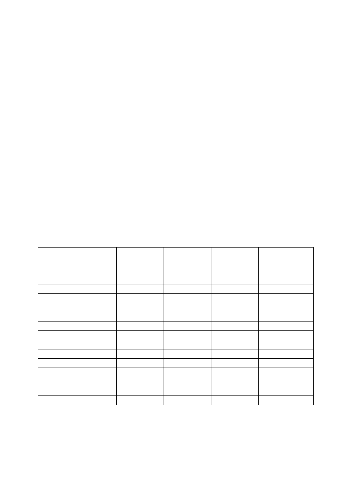
Table 5 YUV received signal formats
No. Definition
1 720×480i/59.94 Hz 15.73 59.94 13.50 CEA-770.2-C
2 720×480i/60 Hz 15.75 60 13.51 CEA-770.2-C
3 720×576i/50 Hz 15.62 50 13.50 ITU-R BT.656–4
4 720×480p/59.94 Hz 31.47 59.94 27.00 CEA-770.2-C
5 720×480p/60 Hz 31.50 60 27.03 CEA-770.2-C
6 720×576p/50 Hz 31.25 50 27.00 ITU-R BT.1358
7 1280×720p/50 Hz 37.50 50 74.25 SMPTE 296M
8 1280×720p/59.94 Hz 44.95 59.94 74.18 CEA-770.3-D
9 1280×720p/60 Hz 45.00 60.00 74.25 CEA-770.3-D
10 1920×1080i/50 Hz 28.12 50 74.25 SMPTE 274M
11 1920×1080i/59.94 Hz 33.72 59.94 74.18 CEA-770.3-C
12 1920×1080i/60 Hz 33.75 60.00 74.25 CEA-770.3-C
13 1920×1080p/50 Hz 56.25 50 148.50
14 1920×1080p/59.94 Hz 67.43 59.94 148.35
15 1920×1080p/60 Hz 67.50 60.00 148.50
H.- Freq.
(kHz)
V.- Freq.
(Hz)
Dot pulse Freq.
(MHz)
Note
5.4 VGA port
Input VGA signal from VG848 with formats listed as Table 6 respectively, check the sound and
the display. If H./V. of picture displays abnormally, enter into user menu Setup→VGA Setting→
AUTO to perform calibration automatically to display the picture fully.
Page 10
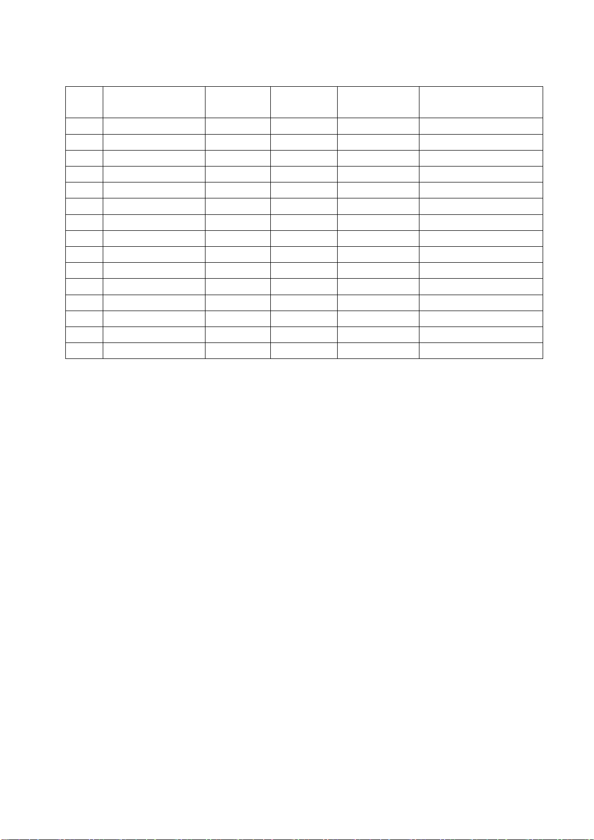
Table 6 VGA received signal formats
No. Definition
1 720×400@70 Hz 31.47 70.08 28.32 VGA-T
2 640×480@60 Hz 31.50 60.00 25.18 VGA
3 640×480@72 Hz 37.90 72.00 31.50 VESA
4 640×480@75 Hz 37.50 75.00 31.50 VESA
5 800×600@56 Hz 35.16 56.25 36.00 VESA
6 800×600@60 Hz 37.90 60.00 40.00 VESA Guidelines
7 800×600@75 Hz 48.08 75.00 50.00 VESA
8 1024×768@60 Hz 48.40 60.00 65.00 VESA Guidelines
9 1024×768@70 Hz 56.50 70.00 75.00 VESA
10 1024×768@75 Hz 60.00 75.00 78.75 VESA
11 1280×768@75 Hz 60.30 75.00 102.25 VESA
12 1360×768@60 Hz 47.70 60.00 85.5 VESA
13 1280×1024@60 Hz 64.00 60.00 108.0 VESA (FHD panel)
14 1280×1024@75 Hz 80.00 75.00 135.0 VESA (FHD panel)
15 1920×1080@60 Hz 67.50 60.00 148.5 CEA-861(FHD panel)
H.- Freq.
(kHz)
V.- Freq.
(Hz)
Dot pulse Freq.
(MHz)
Note
5.5 HDMI port
Input HDMI/DVI signal from VG849 with formats listed as Table 5&6 respectively, check the
sound and the display.
5.6 USB port
Input USB signal, check the sound and the display.
6 Presetting before shipment
Enter into factory menu, select items Other Setting→SHIPMENT to perform presetting before
shipment automatically. The unit only responds the command ‘shut down’ after presetting. The step of
presetting before shipment must be done after factory adjustments completed. Main steps of
SHIPMENT are listed as below:
1)Display guided menu of initial setup when turning on the TV set;
2)Reset default date of picture mode (TV channel picture mode: STANDARD, TV channel color
temperature: NORMAL; VGA channel picture mode: STANDARD, VGA channel color temperature:
COOL; other channels picture mode: COLORFUL, other channels color temperature: COOL); reset
sound mode as SANDARD and the volume as 20;
3)Clear up the date of channel and favorite list;
4)Menu language: simplified Chinese for models of sale in domestic market,
English for export models
Page 11
Software Upgrading Instruction
7 Software Upgrading Instructions as Table 7
Table 7 Software Upgrading Instruction
Location Part No. Part model Software functions
N102 5272532007 EN25Q32B-104HIP Main Software Yes Upgrade with ALL100, etc.
N102 5272532007 EN25Q32B-104HIP HDCP KEY Yes Upgrade with ALL100, etc.
8 Software (FALSH) upgrading methods
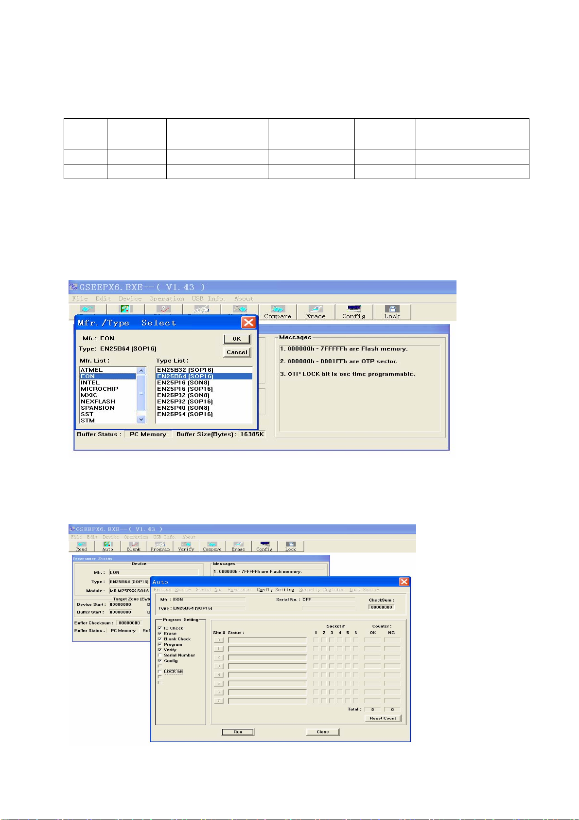
8.1 Execute ALL-100 upgrading file GSEEP.EXE;
8.2 Click menu Device, select FLASH model EN25Q32B shown as Fig. 3;
Note: real FLASH model depends on the real material, models shown by Fig. 3 are just for illustration.
Upgrading
before SMT
Upgrading method
Fig. 3 Device model selection interface
8.3 Click toolbar AUTO, enter into interface AUTO, make sure to tick off option Config when
upgrading Flash. Please refer to Fig. 4.
Fig. 4 AUTO upgrading interface
Page 12
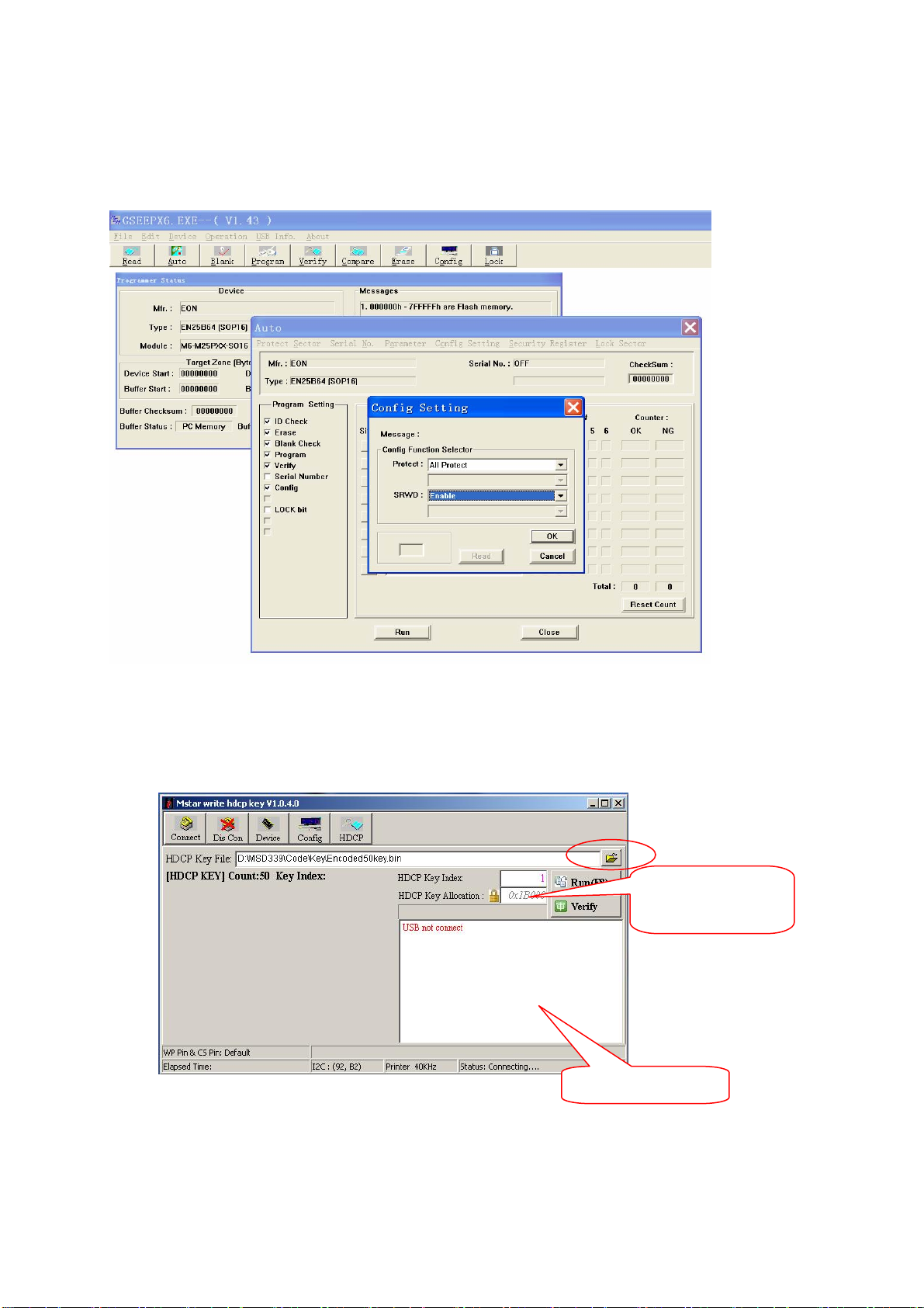
8.4 Click option Config Setting in AUTO interface, set option Protect as All Protect, and set
option SRWD as Enable, then click ‘OK’ to complete write-protect setup. Make sure the above both
options are reset when executing ALL-100 upgrading software again after exiting it. If there is no
option SRWD, please upgrade ALL-100 upgrading software. Please refer to Fig. 5.
Fig. 5 Config Setting interface
9 HDCP KEY upgrading methods
9.1 Connect to upgrading device;
9.2 Execute file ISP_ToolV1.04.exe which interface is shown as Fig. 6;
Location address:
0x3B0000
Fig. 6 ISP tool
9.3 Click button “Open” to load encrypted KEY file;
9.4 Click button “Run” to begin KEY upgrading. upgrading information will display in the information
frame after upgrading completed.
Information frame
Page 13
10 Software upgrading methods
10.1 Software upgrading methods from USB port (it is advise to use the method preferentially)
a) Copy file offered by RD department to the root directory of U disk. Note that the file name must
be MERGE.bin and be kept in the root directory of U disk.
b) Insert U disk to USB port, switch to non-USB channel (such as TV, AV channel, etc.), enter
into factory menu, choose “software upgrading USB”, then click “OK” to begin upgrading;
c) Click “Confirm upgrading” with left button when upgrading confirmation menu displays. Note
that U disk must not be pulled out or the unit must not be cut off during the upgrading process.
10.2 ISP(connected by VGA)upgrading method
a) Connect the unit and PC with upgrading connected board and VGA cable.
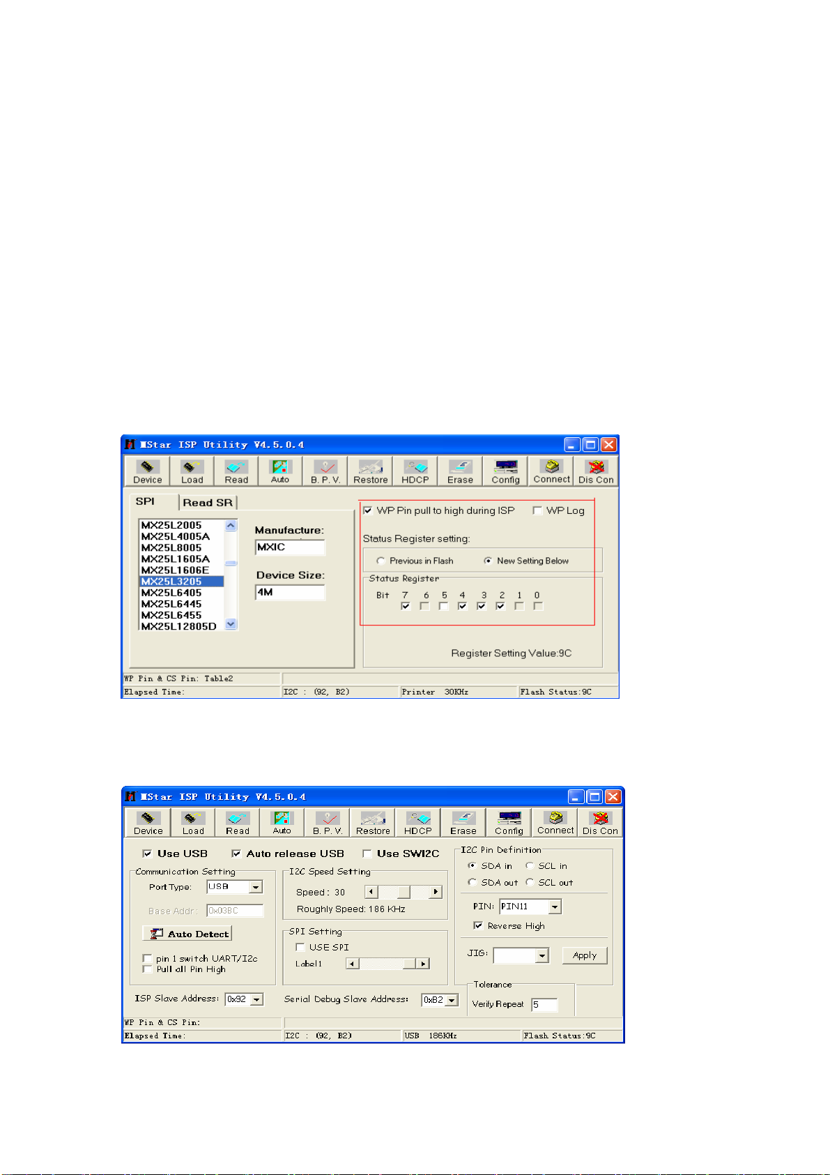
b) Open upgrading tool ISP_Tool(V4.5.0.5), select label Device to make configuration within red
frame shown as Fig. 7;
Fig. 7 Device configuration dialog
c) Select label Config to make configuration shown as Fig. 8;
Fig. 8 Config configuration dialog
Page 14
Note: I2C speed is set as about 60% commonly and should not be set too fast. If it is not easy to
connect successfully, please set I2C speed slower.
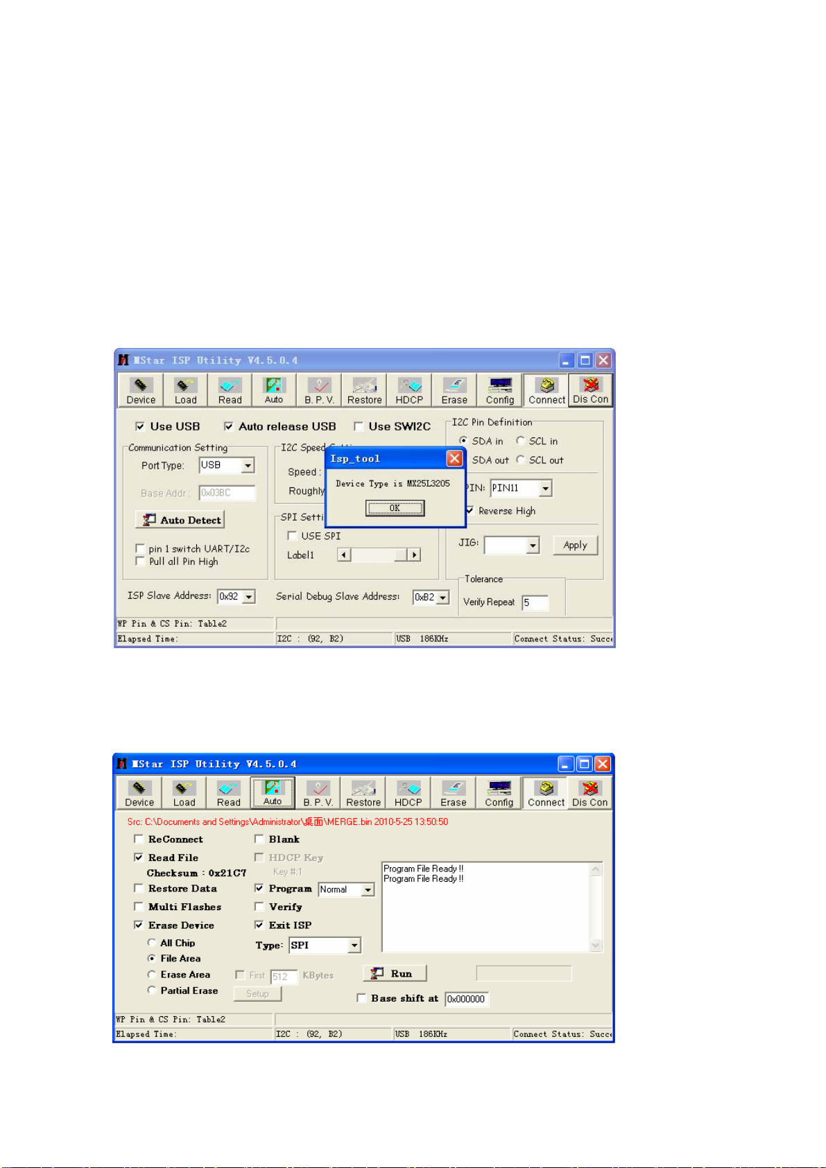
d) Select label Read, open bin file whose file path can display completely in the label Auto,
e) Select label Auto, select items Read File, Erase Device (sub-item File Area of Erase Device
had better be selected), Program and Exit ISP, then click button “Connect”, a dialog shown as Fig. 9
will display if connection is successful, in which device type identified by the system automatically will
display and option “Flash_0” in the static frame “SpiFlash_X” will be ticked off. If device type or
“Flash_0” is not identified correctly, the connection is failed, then ISP tool will repeat identification
automatically until device type and “Flash_0” are identified correctly, if not, please check hardware
connection.
Fig. 9 Successful connect interface
f) Click button “Run” to begin software upgrading after successful connection . Please refer to
Fig. 10;
Fig. 10 Software upgrading interface
Page 15
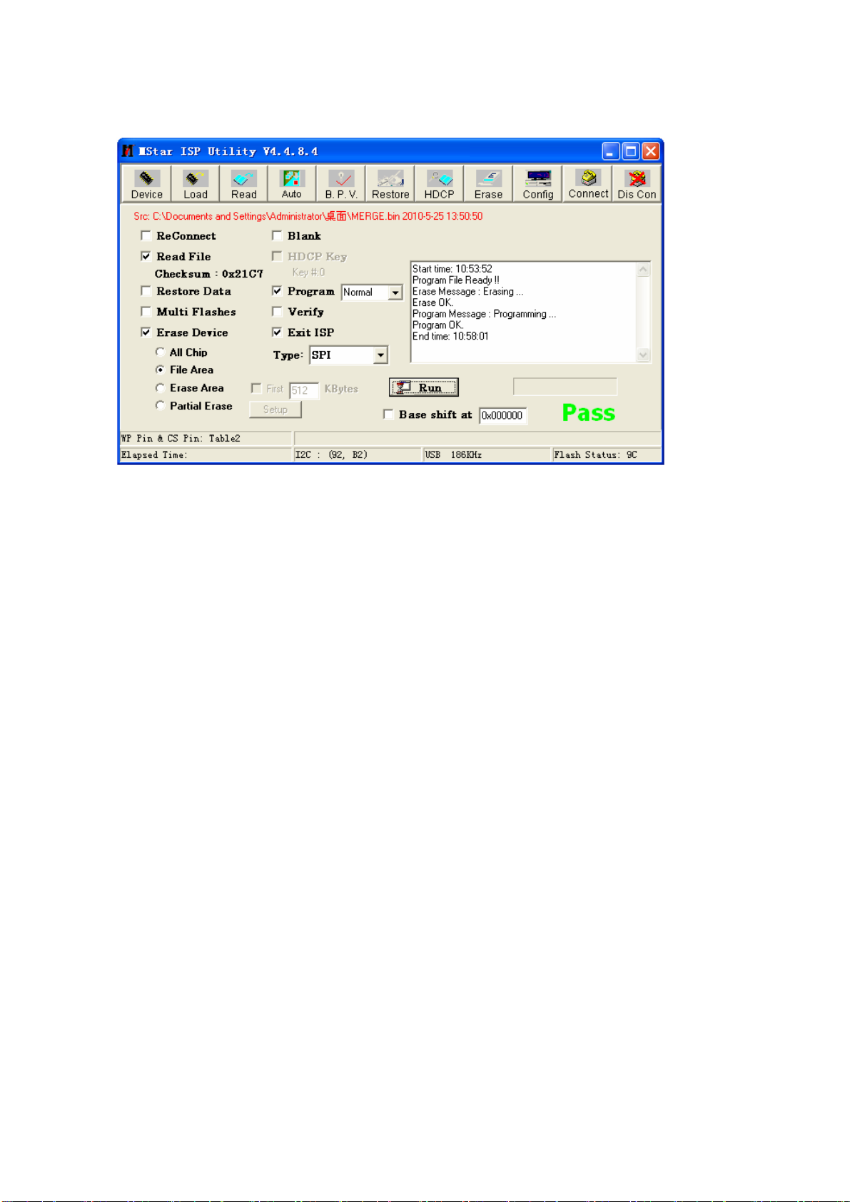
g) Successful software upgrading interface is shown as Fig. 11;
Fig. 11 Successful software upgrading interface
10.3 Software upgrading method from USB port (it is advised to use the method if the picture could
not display because of wrong panel parameters)
a) Copy file offered by RD department to the root directory of U disk. Note that the file name must
be MERGE.bin and be kept in the root directory of U disk.
b) Insert U disk to USB port, keep pressing any key on the key board of the unit except key
“Standby” or “Input”, connect to power supply, switch on power switch of the unit, then IR indicator
light begins twinkling to show the unit is during the upgrading process, unloose the key you press, the
unit will reset automatically after upgrading process completed.
Note that U disk must not be pulled out or the unit must not be cut off during the upgrading
process.
Page 16

Working principle analysis of the unit
RF signal from antenna is sent into Tuner chip N401 to be processed by
HF-amplifier and mixer to get digital IF signal DIF, then DIF signal is sent to
main chip N101(MST6E182VGC).
HDMI signal is sent to HDMI switch chip N201 to be switched by
three-way-signal-selection switch and then sent to main chip N101
(MST6E182VGC).
Video and audio signals from AV, YPbPr , VGA, USB are sent to main chip
N101(MST6E182VGC)directly.
Main chip N101(MST6E182VGC)is a special large scale IC with full functions,
such as HDMI interface processing, video decoding, video switch selection,
A/D and D/A transformation, interleaved/successive scan processing, mode
transformation, OSD and low-voltage difference output processing, etc.;
furthermore, it also has functions of audio selection and audio processing,
MCU, etc.; external video signal is processed by main chip N101
(MST6E182VGC), then 4 pairs of difference signals and one pair of clock
signals are outputted to LCD to display; external audio signal processed by
main chip N101(MST6E182VGC) is sent to sound amplifier N402 to be
amplified and then sent to speakers.
Page 17
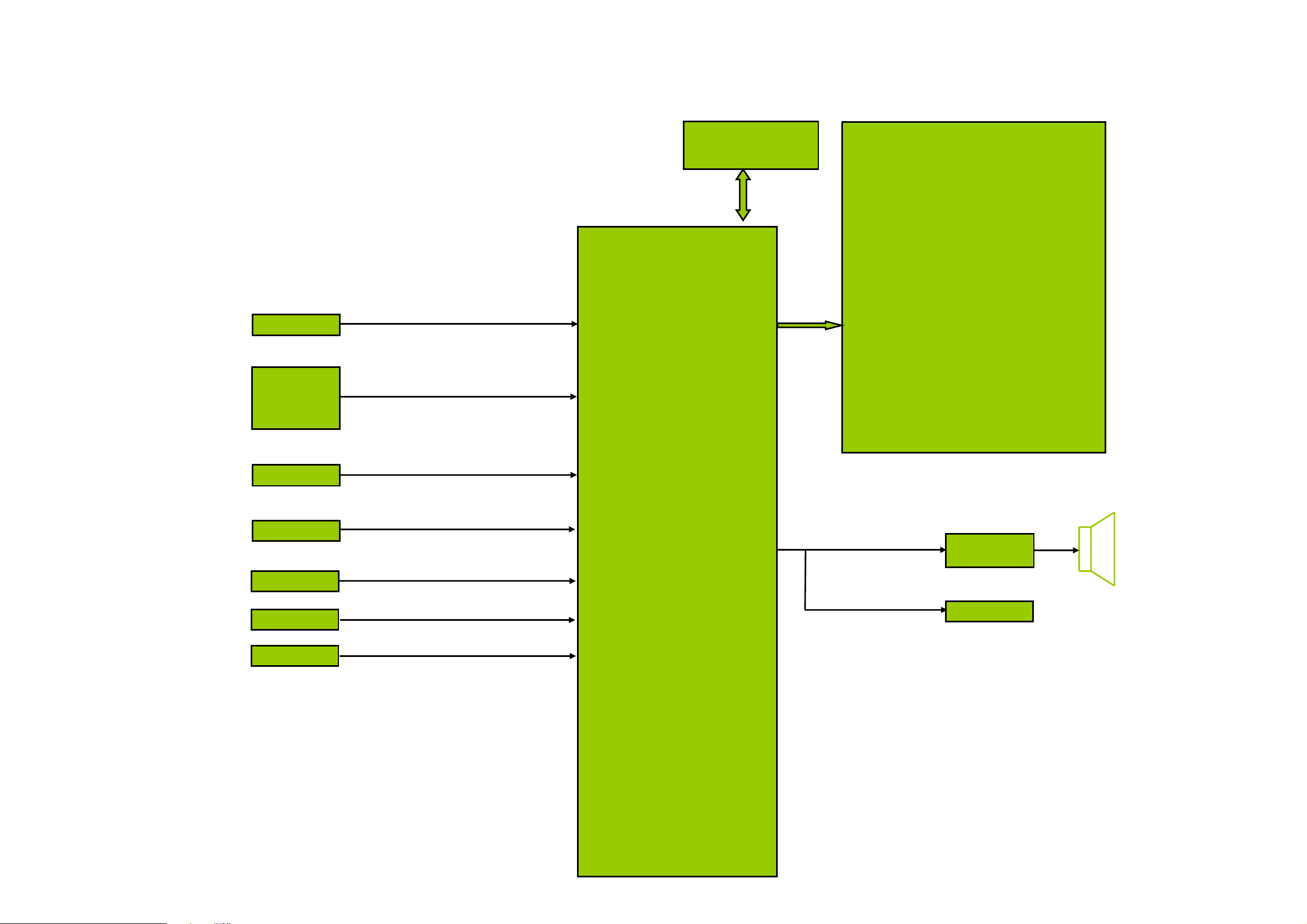
Block Diagram
USB
TUNER
SPI FLASH
Panel
LVDS
AV
YPbPr
VGA
HDMI 1
HDMI 2
MST6E182VG
SPEAKER
AMP
HP
Page 18
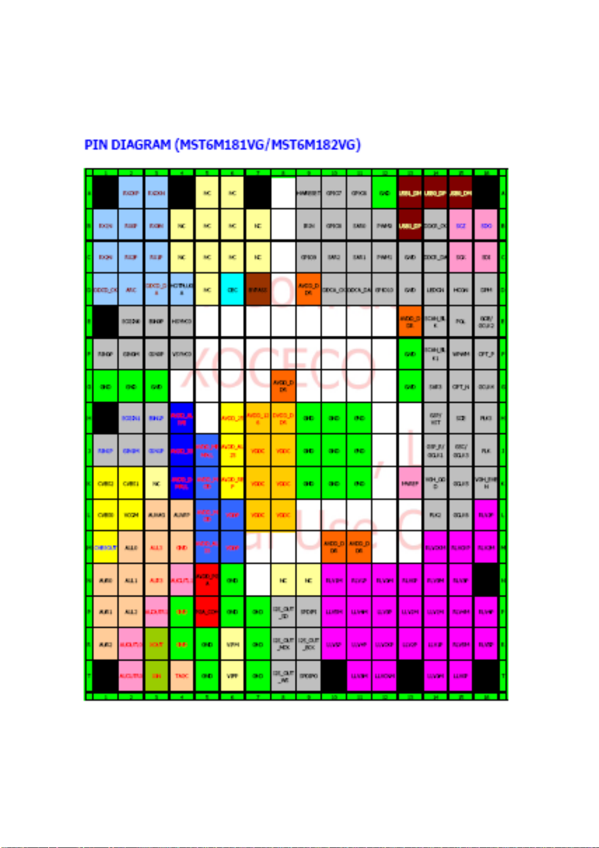
IC Block Diagram
1、 MST6M181VG/MST6M182VG
Page 19
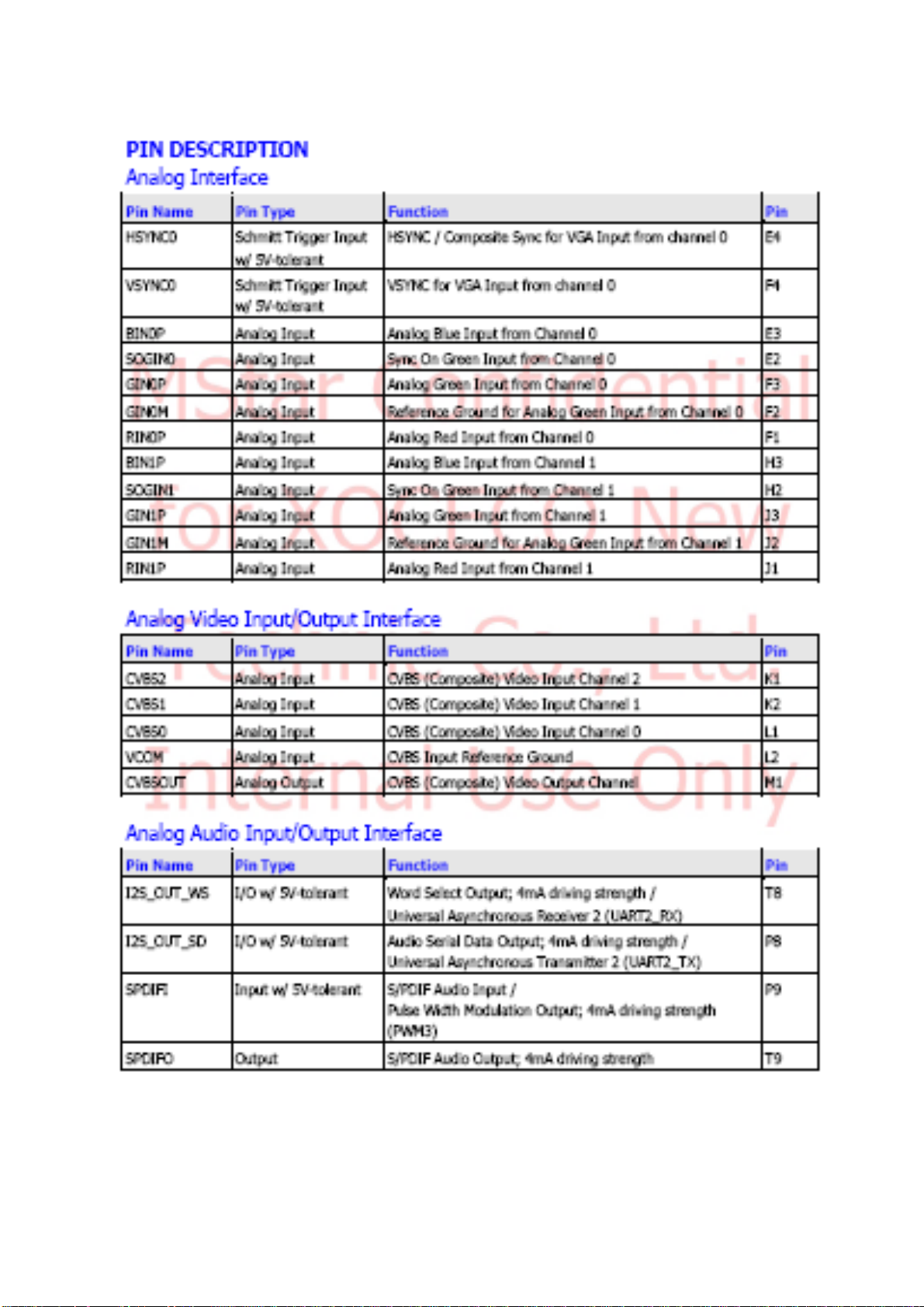
Page 20
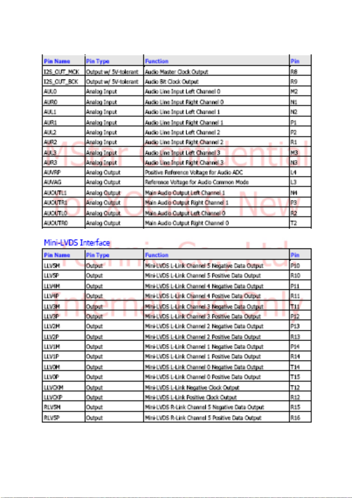
Page 21
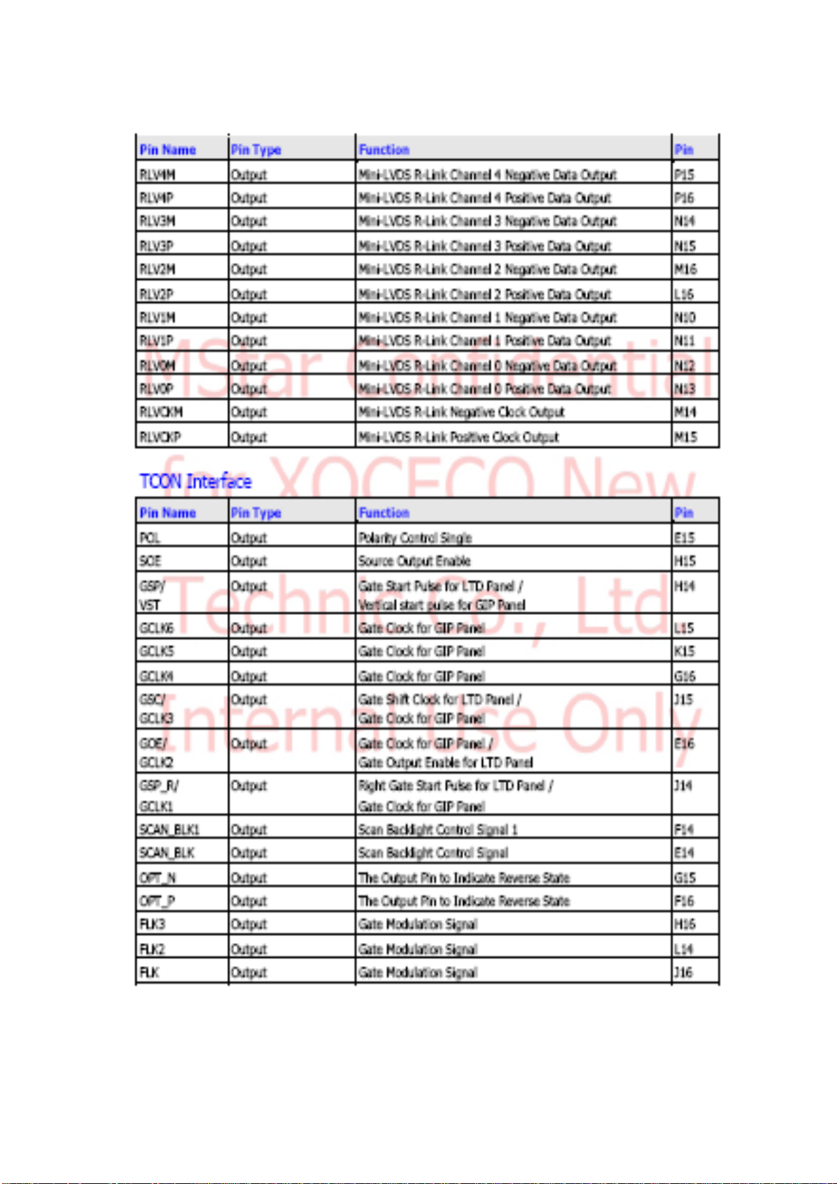
Page 22
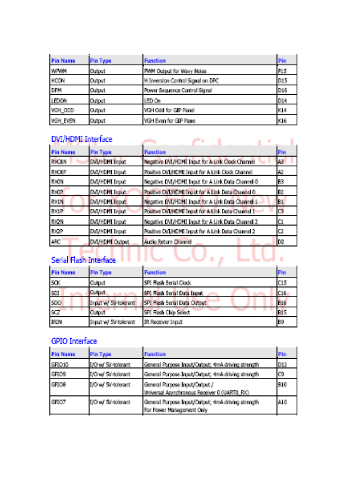
Page 23
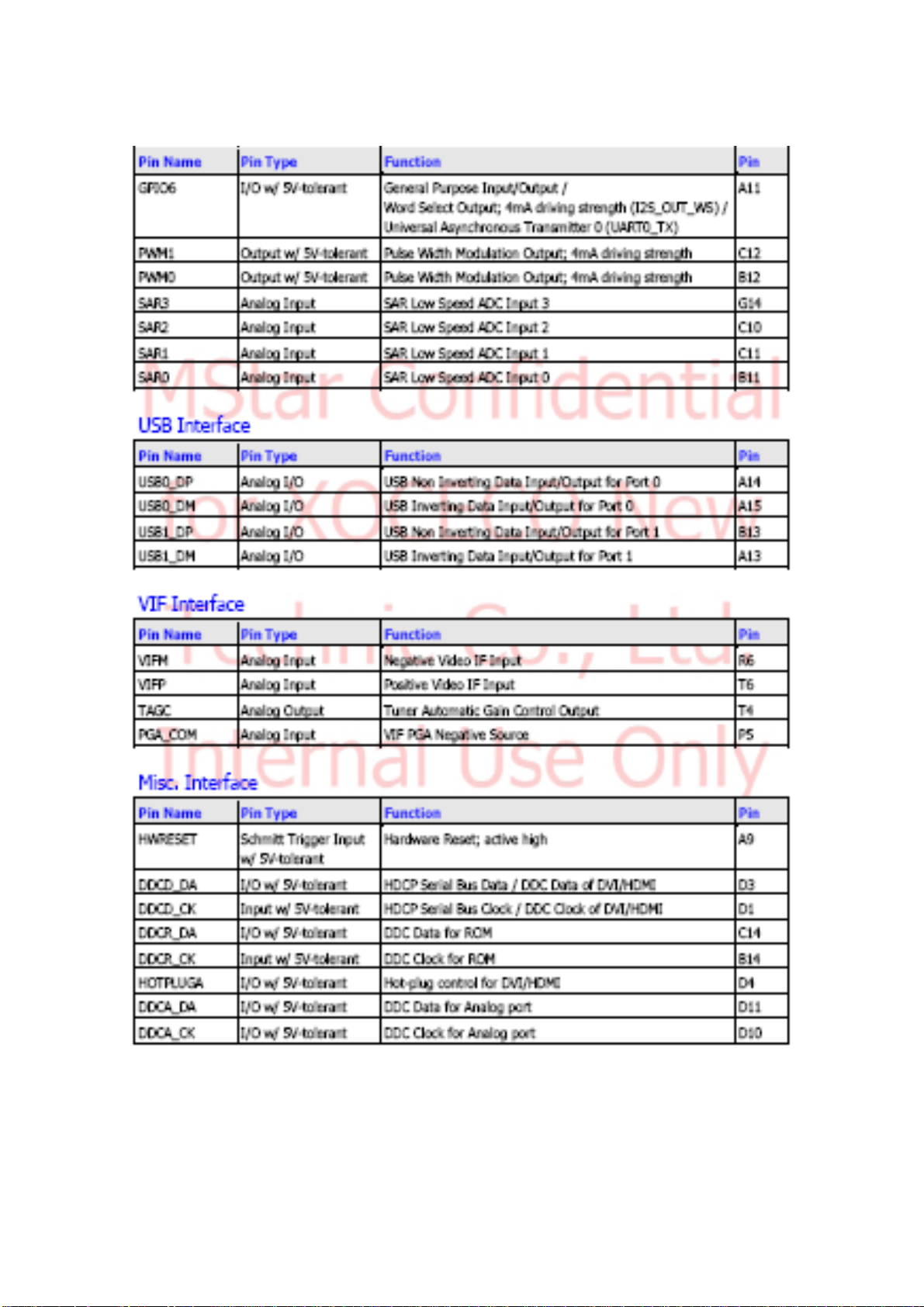
Page 24
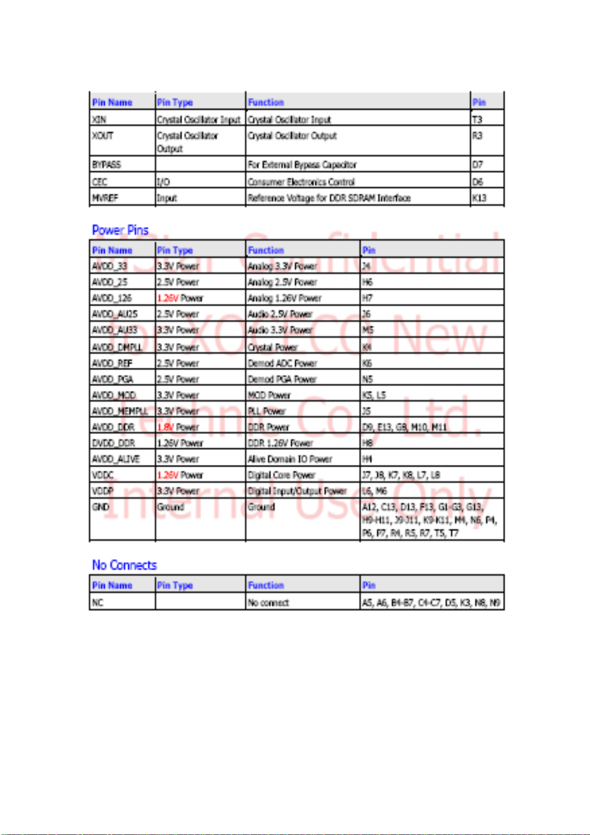
Page 25
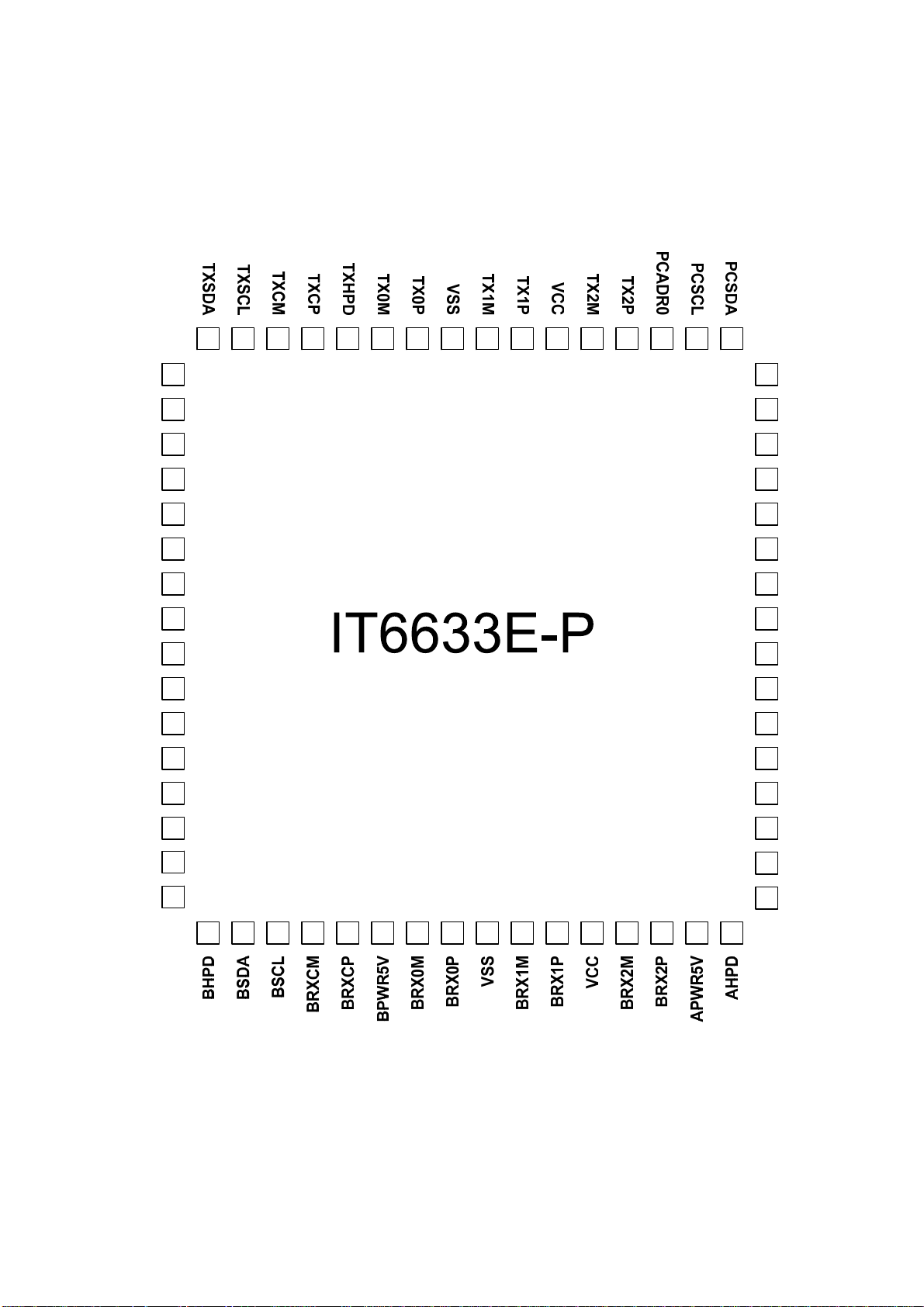
2、 IT6633
Pin Diagram
33343536373839404142434445464748
TXPWR5V
CHPD
CSDA
CSCL
CRXCM
CRXCP
CPWR5V
CRX0M
CRX0P
VSS
CRX1M
CRX1P
VCC
49
50
51
52
53
54
55
56
57
58
59
60
61
32
31
30
29
28
27
26
25
24
23
22
21
20
NC
REXT
ARX2P
ARX2M
NC
ARX1P
ARX1M
VSS
ARX0P
ARX0M
VCC
ARXCP
ARXCM
CRX2M
CRX2P
NC
62
63
64
Figure 1. IT6633 pin diagram
19
ASCL
18
ASDA
17
RESET
16151413121110987654321
Page 26
IT6633
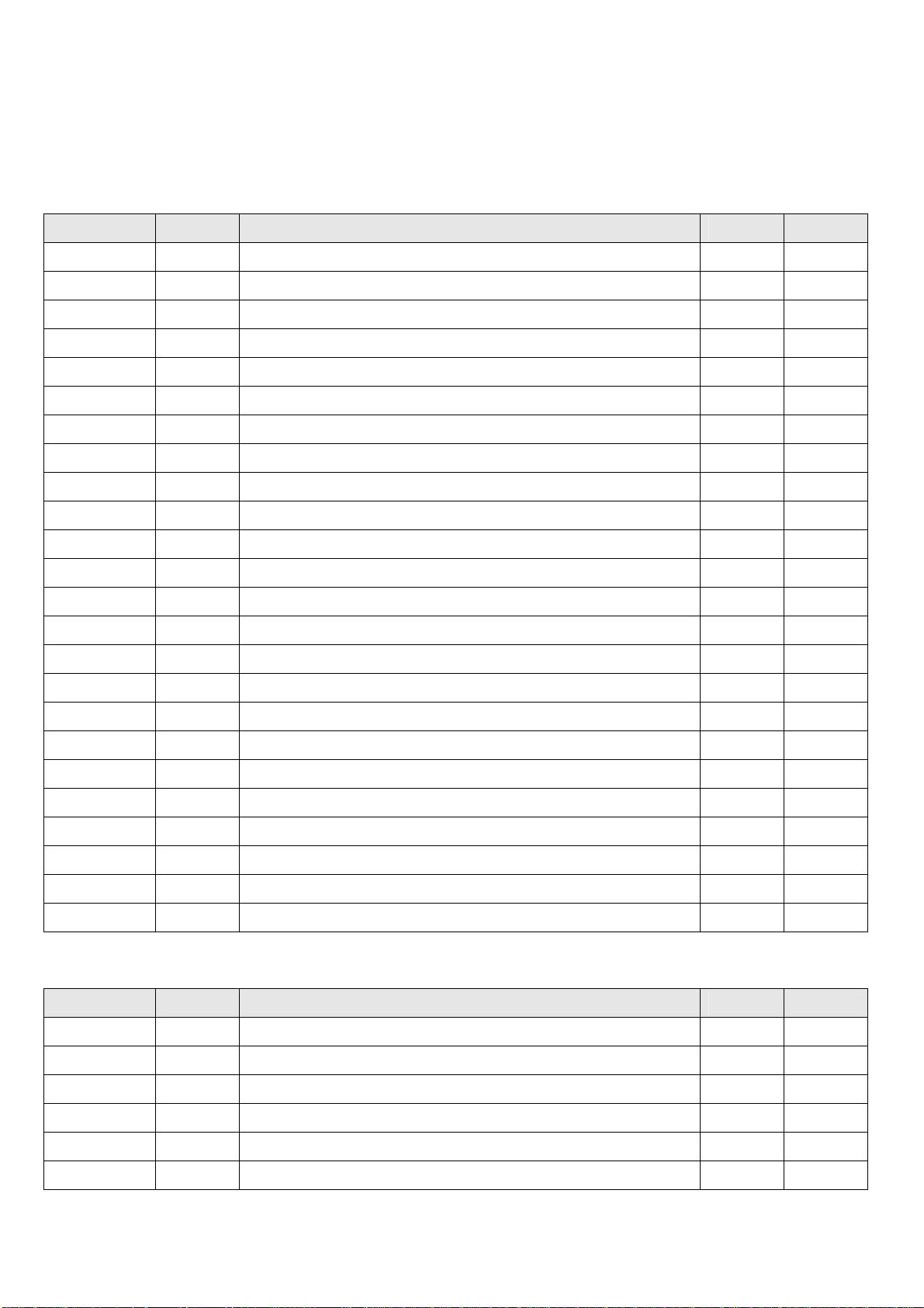
Pin Description
TMDS High Speed Differential Input Pins (All these pins provide ±8kV HBM ESD Protection)
Pin Name Direction Description Type Pin No.
ARX2P Input Channel 2 positive input of Port A TMDS 30
ARX2M Input Channel 2 negative input of Port A TMDS 29
ARX1P Input Channel 1 positive input of Port A TMDS 27
ARX1M Input Channel 1 negative input of Port A TMDS 26
ARX0P Input Channel 0 positive input of Port A TMDS 24
ARX0M Input Channel 0 negative input of Port A TMDS 23
ARXCP Input Clock channel positive input of Port A TMDS 21
ARXCM Input Clock channel negative input of Port A TMDS 20
BRX2P Input Channel 2 positive input of Port B TMDS 14
BRX2M Input Channel 2 negative input of Port B TMDS 13
BRX1P Input Channel 1 positive input of Port B TMDS 11
BRX1M Input Channel 1 negative input of Port B TMDS 10
BRX0P Input Channel 0 positive input of Port B TMDS 8
BRX0M Input Channel 0 negative input of Port B TMDS 7
BRXCP Input Clock channel positive input of Port B TMDS 5
BRXCM Input Clock channel negative input of Port B TMDS 4
CRX2P Input Channel 2 positive input of Port C TMDS 63
CRX2M Input Channel 2 n egative inp ut of Port C TMDS 62
CRX1P Input Channel 1 positive input of Port C TMDS 60
CRX1M Input Channel 1 n egative inp ut of Port C TMDS 59
CRX0P Input Channel 0 positive input of Port C TMDS 57
CRX0M Input Channel 0 n egative inp ut of Port C TMDS 56
CRXCP Input Clock channel positive input of Port C TMDS 54
CRXCM Input Clock channel negative input of Port C TMDS 53
TMDS High Speed Differential Output Pins
Pin Name Direction Description Type Pin No.
TX2P Output Channel 2 positive output of output port TMDS 36
TX2M Output Channel 2 negative output of output port TMDS 37
TX1P Output Channel 1 positive output of output port TMDS 39
TX1M Output Channel 1 negative output of output port TMDS 40
TX0P Output Channel 0 positive output of output port TMDS 42
TX0M Output Channel 0 negative output of output port TMDS 43
Page 27
IT6633
TXCP Output Clock channel positive output of output port TMDS 45
TXCM Output Clock channel negative output of output port TMDS 46
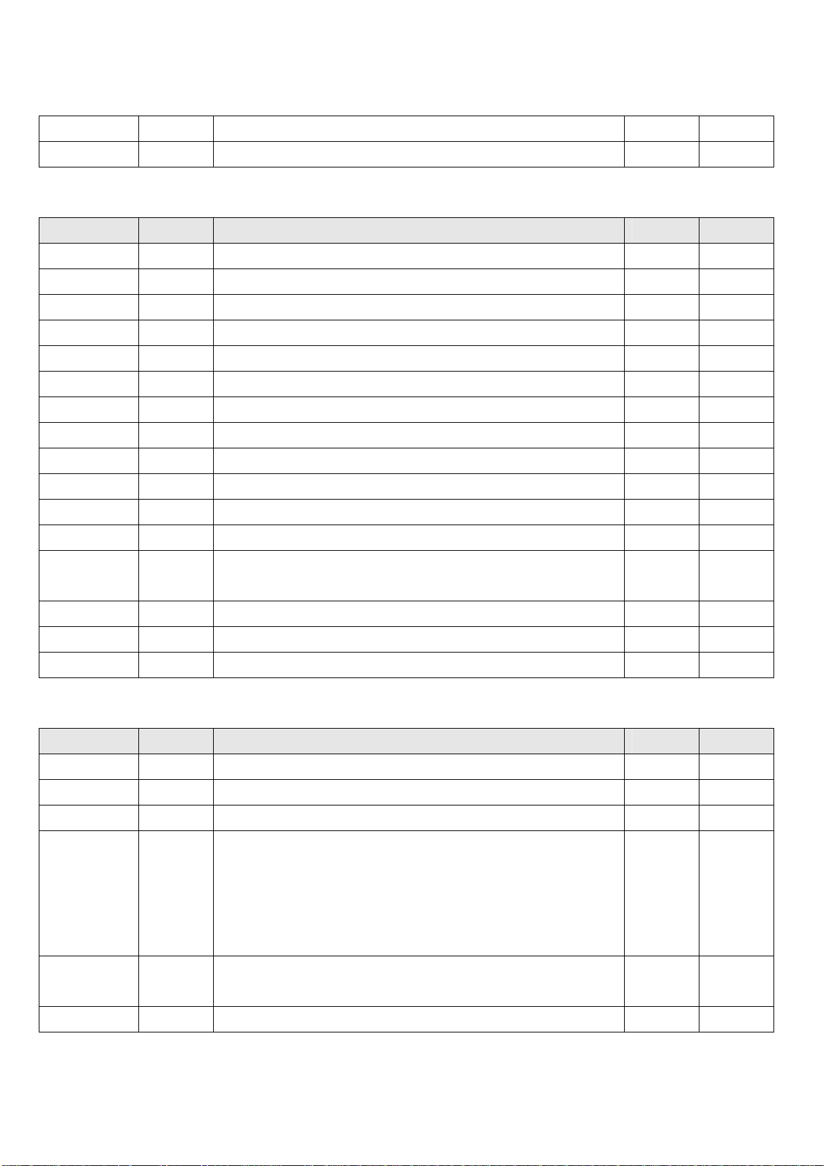
DDC, HPD and PWR5V Control Pins
Pin Name Direction Description Type Pin No.
ASCL I/O Port A DDC bus clock line 5V-Tol. 19
ASDA I/O Port A DDC bus data line 5V-Tol. 18
BSCL I/O Port B DDC bus clock line 5V-Tol. 3
BSDA I/O Port B DDC bus data line 5V-Tol. 2
CSCL I/O Port C DDC bus clock line 5V-Tol. 52
CSDA I/O Port C DDC bus data line 5V-Tol. 51
TXSCL I/O Output Port DDC bus clock line 5V-Tol. 47
TXSDA I/O Output Port DDC bus data line 5V-Tol. 48
TXHPD Input HPD signal of the HDMI Sink 5V-Tol. 44
AHPD Output HPD signal to be sent back to Source connected to Port A LVTTL 16
BHPD Output HPD signal to be sent back to Source connected to Port B LVTTL 1
CHPD Output HPD signal to be sent back to Source connected to Port C LVTTL 50
TXPWR5V Output When ‘1’, indicates that the selected input port has a valid
LVTTL 49
PWR5V input and TMDS clock
APWR5V Input PWR5v of input port A for detection 5V-Tol 15
BPWR5V Input PWR5v of input port B for detection 5V-Tol 6
CPWR5V Input PWR5v of input port C for detection 5V-Tol 55
Other Control and Configuration Pins
Pin Name Direction Description Type Pin No.
RESET Input Reset signals for logic blocks (active-high) LVTTL 17
PCSCL Input Serial programming Clock for chip programming (5V-tolerant) Schmitt 34
PCSDA I/O Serial programming Data for chip programming (5V-tolerant) Schmitt 33
PCADR0 Input Control of serial programming device address:
LVTTL 35
‘0’: 0x94
‘1’: 0x96
(default to ‘0’: 0x94 by internal weak pulled-down resistor of
100kΩ)
REXT Analog External resistor for auto-calibration. Must be tied to VSS via a
Analog 31
500Ω precision resistor.
NC Must be left unconnected 28, 32, 64
Page 28
IT6633
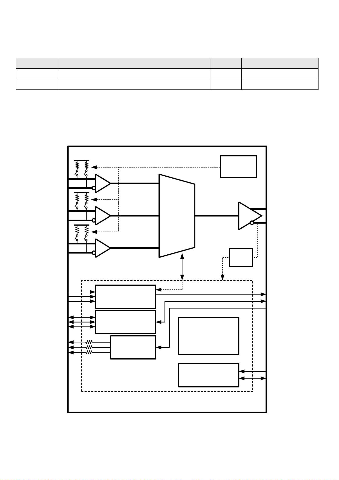
Power and Ground Pins
Pin Name Description Type Pin No.
VCC Chip power supply (3.3V) Power 12, 22, 38, 61
VSS Chip ground Ground 9, 25, 41, 58
Functional Description
Auto-
calibration
ARX[2,1,0,C]P
ARX[2,1,0,C]M
EQ
BRX[2,1,0,C]P
BRX[2,1,0,C]M
CRX[2,1,0,C]P
CRX[2,1,0,C]M
APWR5V
BPWR5V
CPWR5V
ASCL/ASDA
BSCL/BSDA
CSCL/CSDA
AHPD
BHPD
CHPD
EQ
EQ
Active port
indication
DDC I2C Repeater/
Switch
HPD Control
3:1
MUX
Register Block
Control Logic
EDID RAM
and
TX[2,1,0,C]P
DRV
TX[2,1,0,C]M
RX
Detect
TXPWR5V
TXSCL/TXSDA
TXHPD
PCADR0
PCSCL/PCSDA
IT6633E-P Block
Figure 2. Functional block diagram of IT6633
Page 29
SSTIMER
OC_ADJ
PLL_FLTP
VR_ANA
NC
AVSS
PLL_FLTM
BST_A
GVDD_OUT
PVDD_A
OUT_A
RESET
PVDD_A
STEST
PDN
VR_DIG
OSC_RES
DVSSO
DVDD
MCLK
FAULT
SCLK
SDIN
LRCLK
AVDD
SDA
SCL
DVSS
GND
VREG
BST_B
PVDD_B
PVDD_C
OUT_C
PVDD_D
BST_D
PGND_AB
OUT_B
PGND_CD
OUT_D
AGND
PGND_AB
PVDD_B
PGND_CD
PVDD_D
BST_C
PVDD_C
GVDD_OUT
P0075-01
PHP Package
(TopView)
TAS5707
1
2
3
4
5
6
7
8
9
10
11
12
13
14
15 161718 19 20
21 222324
25
26
27
28
29
30
31
32
484746
45 44
43 42 41 40 39 38 37
36
35
34
33
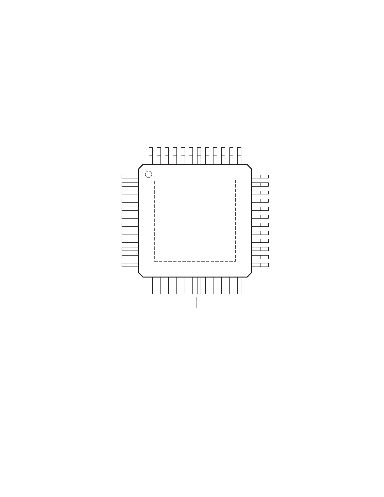
3、 TAS5707, TAS5707A
48-TERMINAL, HTQFP PACKAGE (TOP VIEW)
Page 30
TAS5707, TAS5707A
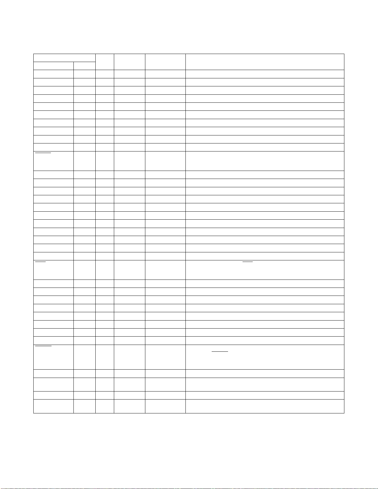
PIN FUNCTIONS
PIN
NAME NO.
AGND 30 P Analog ground for power stage
AVDD 13 P 3.3-V analog power supply
AVSS 9 P Analog 3.3-V supply ground
BST_A 4 P High-side bootstrap supply for half-bridge A
BST_B 43 P High-side bootstrap supply for half-bridge B
BST_C 42 P High-side bootstrap supply for half-bridge C
BST_D 33 P High-side bootstrap supply for half-bridge D
DVDD 27 P 3.3-V digital power supply
DVSSO 17 P Oscillator ground
DVSS 28 P Digital ground
FAULT 14 DO Backend error indicator. Asserted LOW for over temperature, over
GND 29 P Analog ground for power stage
GVDD_OUT 5, 32 P Gate drive internal regulator output
LRCLK 20 DI 5-V Pulldown Input serial audio data left/right clock (sample rate clock)
MCLK 15 DI 5-V Pulldown Master clock input
NC 8 – No connection
OC_ADJ 7 AO Analog overcurrent programming. Requires resistor to ground.
OSC_RES 16 AO Oscillator trim resistor. Connect an 18.2-kΩ 1% resistor to DVSSO.
OUT_A 1 O Output, half-bridge A
OUT_B 46 O Output, half-bridge B
OUT_C 39 O Output, half-bridge C
OUT_D 36 O Output, half-bridge D
PDN 19 DI 5-V Pullup Power down, active-low. PDN prepares the device for loss of power
PGND_AB 47, 48 P Power ground for half-bridges A and B
PGND_CD 37, 38 P Power ground for half-bridges C and D
PLL_FLTM 10 AO PLL negative loop filter terminal
PLL_FLTP 11 AO PLL positive loop filter terminal
PVDD_A 2, 3 P Power supply input for half-bridge output A
PVDD_B 44, 45 P Power supply input for half-bridge output B
PVDD_C 40, 41 P Power supply input for half-bridge output C
PVDD_D 34, 35 P Power supply input for half-bridge output D
RESET 25 DI 5-V Pullup Reset, active-low. A system reset is generated by applying a logic low
SCL 24 DI 5-V I2C serial control clock input
SCLK 21 DI 5-V Pulldown Serial audio data clock (shift clock). SCLK is the serial audio port input
SDA 23 DIO 5-V I2C serial control data interface input/output
SDIN 22 DI 5-V Pulldown Serial audio data input. SDIN supports three discrete (stereo) data
TYPE 5-V TERMINATION
(1)
TOLERANT
(2)
DESCRIPTION
current, over voltage, and under voltage error conditions. De-asserted
upon recovery from error condition.
supplies by shutting down the noise shaper and initiating PWM stop
sequence.
to this pin. RESET is an asynchronous control signal that restores the
DAP to its default conditions, and places the PWM in the hard mute
state (tristated).
data bit clock.
formats.
Page 31
TAS5707, TAS5707A
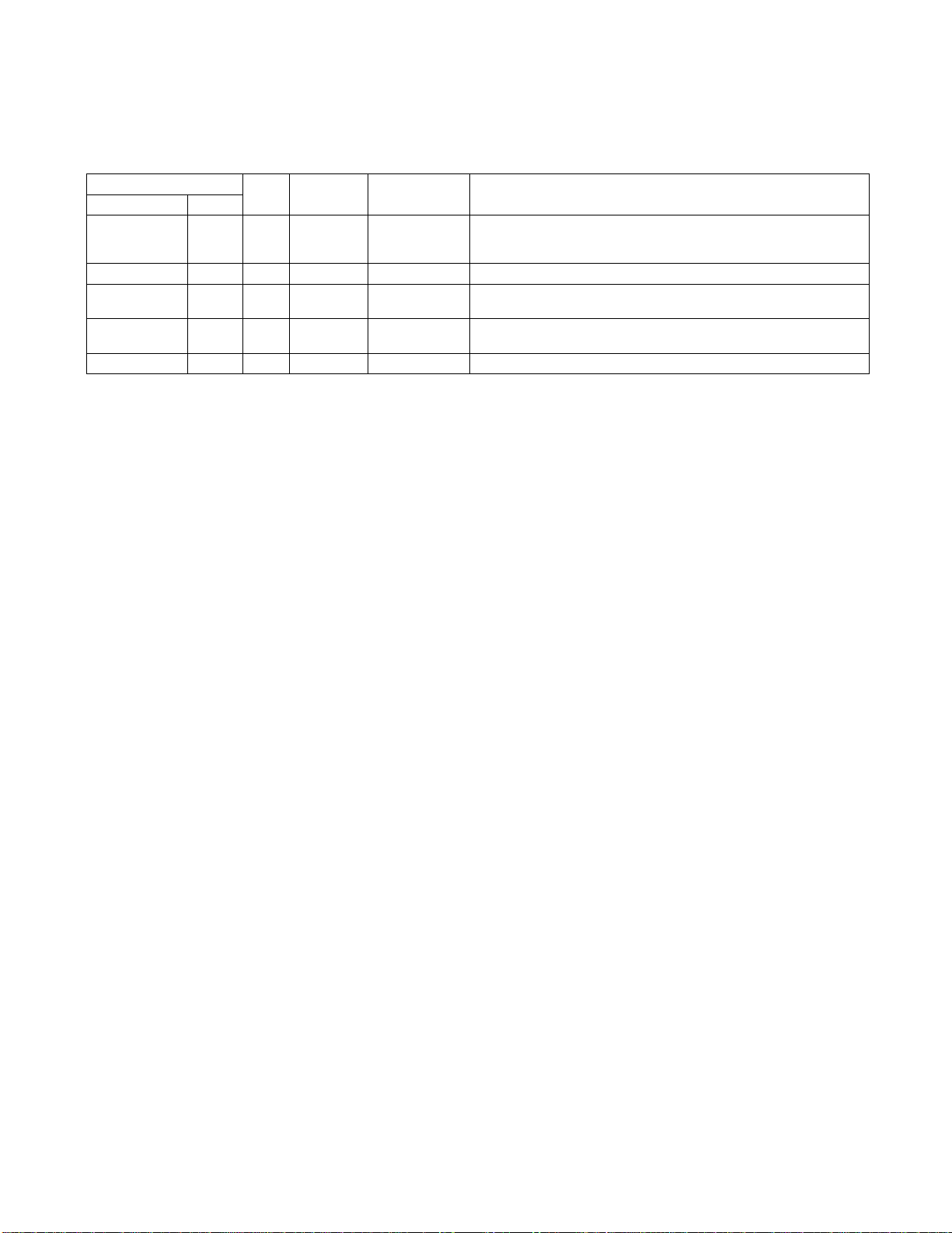
PIN FUNCTIONS (continued)
PIN
NAME NO.
SSTIMER 6 AI Controls ramp time of OUT_X to minimize pop. Leave this pin floating
STEST 26 DI Factory test pin. Connect directly to DVSS.
VR_ANA 12 P Internally regulated 1.8-V analog supply voltage. This pin must not be
VR_DIG 18 P Internally regulated 1.8-V digital supply voltage. This pin must not be
VREG 31 P Digital regulator output. Not to be used for powering external circuitry.
TYPE 5-V TERMINATION
(1)
TOLERANT
(2)
DESCRIPTION
for BD mode. Requires capacitor of 2.2 nF to GND in AD mode. The
capacitor determines the ramp time.
used to power external devices.
used to power external devices.
Page 32
Wiring Diagram
Panel
Power board assembly
Key board assembly
Main board assembly
IR board assembly
Page 33
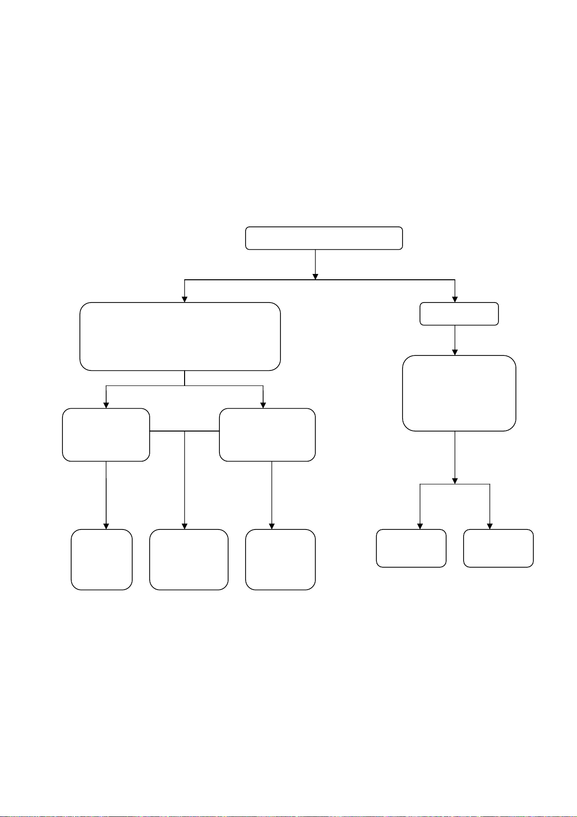
Troubleshooting flow chart
r
1. No raster, no picture, no sound.
Yes No
Press button POWER of remote control or unit to
turn on the TV set, then check if X301-5#/6#
(12V), X301-10# (5V) are normal or not?
No raster, no picture, no sound
Does power indicator light up?
Check 5V_STB
Disconnect power
Yes No
Is the voltage of
No No
X301-13# on main
board high level?
Is the voltage of
X301-9# on main
board high level?
board from data
processing board, then
test 5V_STB again.
Yes Yes Yes No
Check
backlight
board
Check
N101and its
power circuits
Check
power board
assembly
Check
main board
Check power
boa
d
Page 34
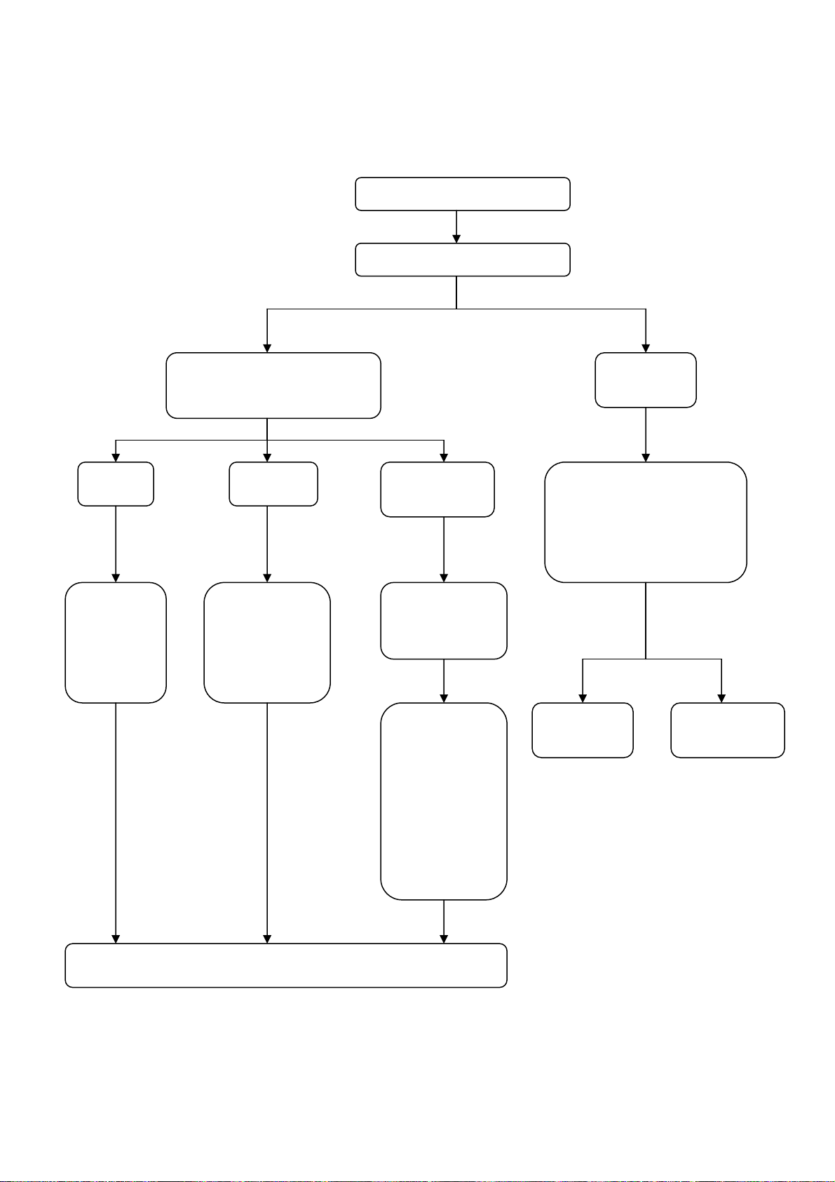
2. No picture, but sound is normal.
r
p
p
Yes No
Check if current channel that
OSD displays is normal or not?
HDMI
USB
No Yes
Check if
N102(KEY)
is normal or
not?
Check if 5V
supplied for USB
channel is
normal or not?
Check N101 and its power circuits
No picture, but sound is normal.
Are LOGO and OSD normal?
TV/AV/VGA/
YPbP
Check if signal
input is normal or
Switch to TV
channel, check
power supply,
I2C BUS and
pin12/13 output
of TUNER chip
are normal or
not?
Check LVDS
connection
Check if power voltage of
panel backlight and backlight
control pin X301-13# (3V) are
normal or not?
Power board
roblem
has
PANEL has
roblem.
Page 35
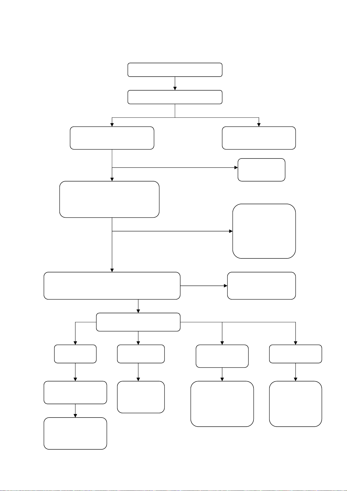
3. No sound, but the picture is normal.
p
r
p
p
No Yes
Check power 12/24V supplied
fo
C302 is normal or not?
No
Yes
Check if there is signal inputted to
power amplifier N402, check if MUTE
and power of N402 are normal or not?
No sound, but the picture is normal.
Check if there is output from X402?
Connection to speakers or
s
eakers have problem.
Power board
roblem.
has
Check if power
Yes
amplifier N402 and
power of control
circuits are normal or
not?
No
Yes
Check if output of N101-P8/R9/R8/T8 are normal or
not and check if the voltage of N101-J16 is high level?
Check if power amplifier
N402 is normal or not?
No
Check current channel.
TV channel
Check if there is
ut from AVOUT ?
out
Check if DIF output
circuits of TUNER is
无
USB channel
Check if file
format is
YPbPr ,VGA,
AV channel
Check if there is
signal inputted to
corresponding
terminal of N101?
HDMI channel
Check if HDMI
N102(KEY) is
normal or not?
Page 36
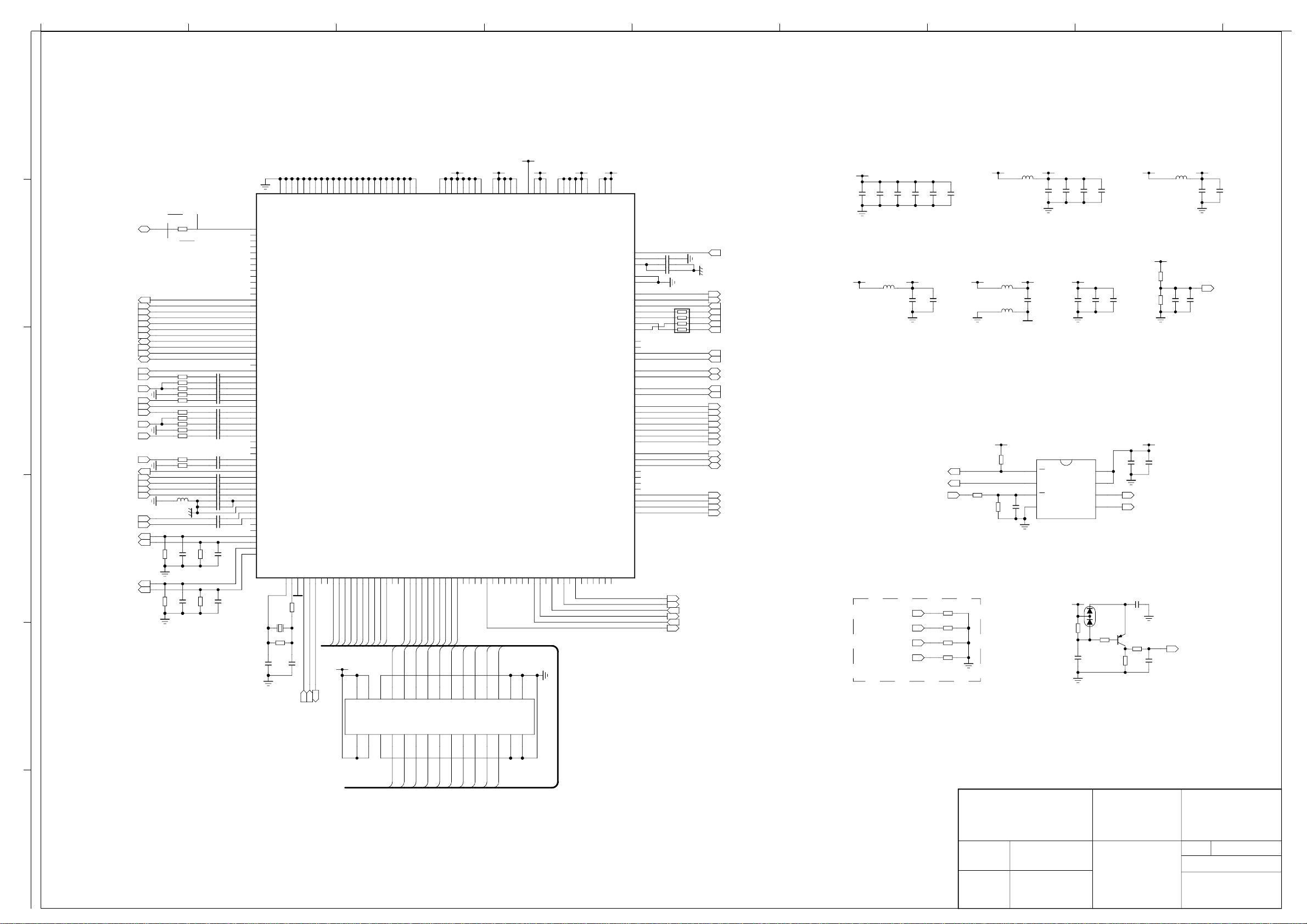
ABCDEFGH
1
2.5V_PGA
L103
1.8V_DDR21.2V
G13
L8
K8
G3
T5
P4
G1
G2
R5
R4
GND
GND
GND
GND
GND
GNDP6GNDT7GNDH9GND
R133
002:A1;002:A2
CEC
200
NC
2
HDMI_HPD002:E1
HDMI_RXC-
002:E1
HDMI_RXC+
002:E1
HDMI_RX0-
002:E2
HDMI_RX0+
002:E2
HDMI_RX1-
002:E2
HDMI_RX1+
002:E2
HDMI_SDA
002:E1
HDMI_RX2-
002:E2
HDMI_RX2+
002:E2
HDMI_SCL
002:E1
002:B4
VGA_HS
002:B4
VGA_B+
002:B4
VGA_G+
002:B4
3
002:B4
002:G1
002:H2
002:G1
002:G1
002:B5
002:B5
002:H3
002:H3
VGA_R+
VGA_VS
YPBPR_PB002:D4
YPBPR_Y002:D4
YPBPR_PR002:D5
AV_V
AVOUT_V
AV_L
AV_R
VGA_L
VGA_R
YPBPR_L002:D5
YPBPR_R002:D5
AVOUT_L
AVOUT_R
4
HPOUT_L
002:G5
002:G5
HPOUT_R
R103 33
R104 33
R105 33
R106
R107 33
R108 33
R109 33
R110 33
R111
R112 33
R113 33
R114
120ohm
L101
R101
100K
R102
100K
50V
50V
C103
C104
C105
68
C106
C107
C108
C109
C110
68
C111
C112
C113
68
C114
C118
C119
C120
C121
C115
C122
3A
C123
C124
100K
R115
C101
180p
100K
R116
C102
180p
50V
50V
47n
1n
47n
47n
47n
47n
1n
47n
47n
47n
47n
47n
2.2u
2.2u
2.2u
2.2u
10u
100n
2.2u
2.2u
C116
180p
C117
180p
D6
D5
C7
B7
C6
B6
A6
C5
C4
A5
B5
B4
D4
A3
A2
B3
B2
B1
C3
D3
C1
C2
D1
D2
E4
E3
E2
F3
F2
F1
F4
H3
H2
J3
J2
J1
K3
K1
K2
L1
L2
M1
M2
N1
N2
P1
L3
M4
P2
R1
M3
N3
N4
P3
R2
T2
CEC
HOTPLUGD
RXCKN_D
RXCKP_D
RX0N_D
RX0P_D
RX1N_D
RX1P_D
DDCDD_DA
RX2N_D
RX2P_D
DDCDD_CK
HOTPLUGA
RXCKN_A
RXCKP_A
RX0N_A
RX0P_A
RX1N_A
RX1P_A
DDCDA_DA
RX2N_A
RX2P_A
DDCDA_CK
ARC
HSYNC0
BIN0P
SOGIN0
GIN0P
GIN0M
RIN0P
VSYNC0
BIN1P
SOGIN1
GIN1P
GIN1V
RIN1P
VSYNC1
CVBS2
CVBS1
CVBS0
VCOM
CVBSOUT
AUL0
AUR0
AUL1
AUR1
AUVAG
AUREFM
AUL2
AUR2
AUL3
AUR3
AUOUTL1
AUOUTR1
AUOUTL0
AUOUTR0
G101
24MHz
R117
50V
20p
C125
XINR3XOUTP5PGA-COMR6VIFMT6VIFPT4RFAGC
T3
0
R118
1M
50V
20p
C126
R7
GND
GNDP7GND
B_ODD0/LVA4P
B_ODD1/LVA4M
B_ODD2/LVA3P
B_ODD3/LVA3M
P10
R10
P11
R11
T11
RXE3+
RXE3-
VCC_PANEL
H10
J10
H11
J9
GND
GND
GND
B_ODD4/LVACLP
B_ODD5/LVACKM
B_ODD6/LVA2P
B_ODD7/LVA2M
P12
T12
R12
P13
RXEC+
RXEC-
RXE2+
RXE2-
RXE1+
F13
J11
K10
K9
K11
A12
GND
GND
GND
GND
GND
GND
G_ODD0/LVA1P
G_ODD1/LVA1M
G_ODD2/LVA0P
G_ODD3/LVA0M
G_ODD4/LVB4P
G_ODD5/LVB4M
R13
P14
R14
T14
T15
R15
RXE1-
RXE0+
RXE0-
RXO3+
RXO0-
RXO1-
GND
G_ODD6/LVB3P
R16
RXO3-
L7
GNDN6GND
VDDC
VDDCJ8VDDC
VDDCK7VDDCH8VDDC
1.26V
N101
MST6M182VG
R_ODD0/LVBCKP
G_ODD7/LVB3M
R_ODD1/LVBCKM
R_ODD2/LVB2P
R_ODD3/LVB2M
R_ODD4/LVB1P
R_ODD5/LVB1M
R_ODD6/LVB0P
P15
P16
N14
N15
M14
M15
M16
L16
RXOC+
RXOC-
RXO2+
RXO2-
RXO1+
RXO1-
RXO0+
RXO0-
RXO2-
RXOC-
RXO3-
RXE0-
G8
J7
D9
H7
E13
M11
M10
N5
VDDC
AVDD_DDR
AVDD_DDR
AVDD_DDR
AVDD_DDR
AVDD_1P2
AVDD_DDR
DDR1 2.5V
DDR2 1.8V
R_ODD7/LVB0M
GPIO21/TCON21/VGH_ODD_49
GPIO20/TCON20/VGH_EVEN_48
GPIO19/TCON19/GCLK6_47
GPIO18/TCON18/GCLK5_46
GPIO17/TCON17/GCLK4_45
GPIO16/TCON16/WPWM_44
GPIO15/TCON15/SCAN_BLK1_43
GPIO14/TCON14/SCAN_BLK_42
GPIO13/TCON13/LEDON_41
GPIO12/TCON12/DPM_40
GPIO11/TCON11/HCON_39
K14
K16
L15
K15
G16
F15
F14
E14
D14
D16
D15
G15
RXE1-
RXE2-
RXEC-
RXE3-
H6
K6
J6
J5
AVDD_25
AVDD_PGA
AVDD_REF
AVDD_AU25M5AVDD_AU33
2.5V 3.3V
GPIO define
MST6M161LG/MST6M181VG
MST6M182VG
GPIO10/TCON10/OPT_N_38
GPIO9/TCON9/OPT_P_37
GPIO8/TCON8/FLK3_36
GPIO7/TCON7/FLK2_35
GPIO6/TCON6/FLK_34
GPIO5/TCON5/SOE_33
F16
H16
L14
J16
H15
J15
AVDD_33_PMAVDD_33ADC2P5
L5
J4
K4
H4
AVDD_33
AVDD_MODK5AVDD_MODM6AVDD_MODL6AVDD_MOD
AVDD_PLL
PMGPIO_GPIO10/GPIO66
SAR3_GPIO14/INT_GPIO65
GPIO4/TCON4/GCLK3_32
GPIO3/TCON3/GCLK2_31
GPIO2/TCON2/GCLK1_30
E16
J14
H14
AVDD_DVI
AVDD_DMPLL
MVREF
DVDD_NODIE
VRP
GND_EFUSE
TESTPIN
SAR2_GPIO13/GPIO73
SAR1_GPIO12/GPIO74
SAR0_GPIO11/GPIO75
PWM0_GPIO20/GPIO26
PWM1_GPIO21/GPIO25
PM1_GPIO6/GPIO67
PM4_GPIO7/GPIO68
PM5_GPIO8/GPIO69
PM6_GPIO9/GPIO70
GPIO0/TCON0/POL_28
GPIO1/TCON1/VST_29
E15
SCZ
SDO
SDI
SCK
USB1_DP
USB1_DM
USB0_DP
USB0_DM
DDCA_DA
DDCA_CK
IRIN
HWRESET
DDCR_CK/GPIO63
DDCR_DA/GPIO64
NC/GPIO62
GPIO26/GPIO61
GPIO27/GPIO60
NC/GPIO59
GPIO23/GPIO58
GPIO25/GPIO57
GPIO24/GPIO56
GPIO22/GPIO56
GPIO30/LCK_74
GPIO29/LDE_75
GPIO28/LHSYNC
GPIO27/LVSYNC
N10
N11
N12
N13
K13
D7
L4
D13
C13
C10
C11
B11
B15
B16
C16
C15
B13
A13
A14
A15
D11
D10
B9
A9
B12
C12
D12
A11
A10
B10
C9
G14
B14
C14
N9
P9
T9
N8
P8
R9
R8
T8
2.2u
10u
100n
C127
C129
C128
33
R119
TCON2
TCON4
HP_DETE
AMP_RESET
HDMI_EN
HDMI_RESET
001:G4
001:G5
002:F5
004:F4
002:E1
MVREF 001:H2
AMP_STB
LED
KEY
SPI_CZ
SPI_DO
SPI_CK
SPI_DI
USB_D+ 002:B6
USB_D-
VGA_SDA_TXD
VGA_SCL_RXD
003:B5
IRIN
RESET
001:G5;003:B1
PWM
CFG_PWM1 001:G5
FLASH_WP 001:G4
PANEL_ON 003:D5
POWER_ON
BL_ON 003:B1
MUTE_PHOUT
EOP_PWON
TUNER_SCL
TUNER_SDA
SDIN
SCLK
MCLK
LRCLK
002:B3
004:E2
003:B5
003:B4
001:G3
001:G4
001:H4
001:H4
002:B6
002:B4
002:B4
001:H5
003:B2;003:D2;003:D4;003:H2
002:F4
002:H4
002:E2;004:B4;004:F4
002:E2;004:B4;004:F4
004:F4
004:F3
004:F3
004:F3
1.2V
6.3V
10u
C130
C131
L102
120ohm
250mA
001:E4
001:E4
001:E3
CHIP CONFIG
100n
C132
3A
TCON2
TCON4
CFG_PWM1
PWM001:E3;003:B1
C133
100n
100n
001:E2
001:E2
FLASH_WP001:E3
POWER ON LOW
100n
C136
SPI_CZ
SPI_DO
C134
100n
100n
R120
4.7K
R121
4.7K
R122
4.7K
R123
4.7K
C135
C137
3.3V AVDD_33_PM3.3V_STB
100n
L104
120ohm
L105
120ohm
3.3V_STB 3.3V_STB
4.7K
R126
1K
R124
10K
R125
AVDD_33
120ohm
3A
6.3V
2.5V_PGA2.5VADC2P52.5V
3A
100n
3A
C141
C143
5272532007 OR 5273206001
EN25Q32B-104HIP
1
CS
2
DO/DQ1
3
WP/DQ2
4
VSS
100n
10u
C138
1.8V_DDR2
N102
C139
100n
6.3V
NC/DQ3
DI/DQ0
5V_STB
100K
R127
10V
10u
VCC
CLK
2.2u
C140
C144
C145
100n
C142
100n
C146
100n
8
7
6
5
D101
LBAV99LT1G
10K
R128
C148
47K
R129
100n
100n
C152
C151
SPI_CK
SPI_DI
C150
2.2u
10V
V101
BC857AW
R130
100
120ohm
1.8V_DDR2
1K
R131
1K
R132
10u
6.3V
001:E2
001:E3
1n
C153
1n
C154
L107
3A
100n
C155
RESET
C156
001:E3
100n
MVREF
C157
100n
001:E2
23
25
27
23
24
25
26
26
RXE3+
29
27
29
28
30
28
30
3
5
1
AGC
VIFM
VIFP
X101
004:D3
PHB-2x15-2.0
004:D4
004:D4
2
7
5
3
1
2
4
4
6
11
9
7
5
9
10
6
8
8
10
12
RXO0+
RXO1+
RXO2+
17
19
15
13
11
13
12
14
14
16
RXOC+
RXO3+
21
17
19
18
18
RXE0+
20
20
RXE1+
21
22
22
RXE2+
24
RXEC+
15
16
TITLE: DWG NO.
MAIN CHIP 9232ME7001DL
6
DRAWN BY
APPROVED BY
REV.
Sheet to
1
A1.0
4
XOCECO
XIAMEN OVERSEAS CHINESE
ELECTRONIC CO., LTD.
Page 37
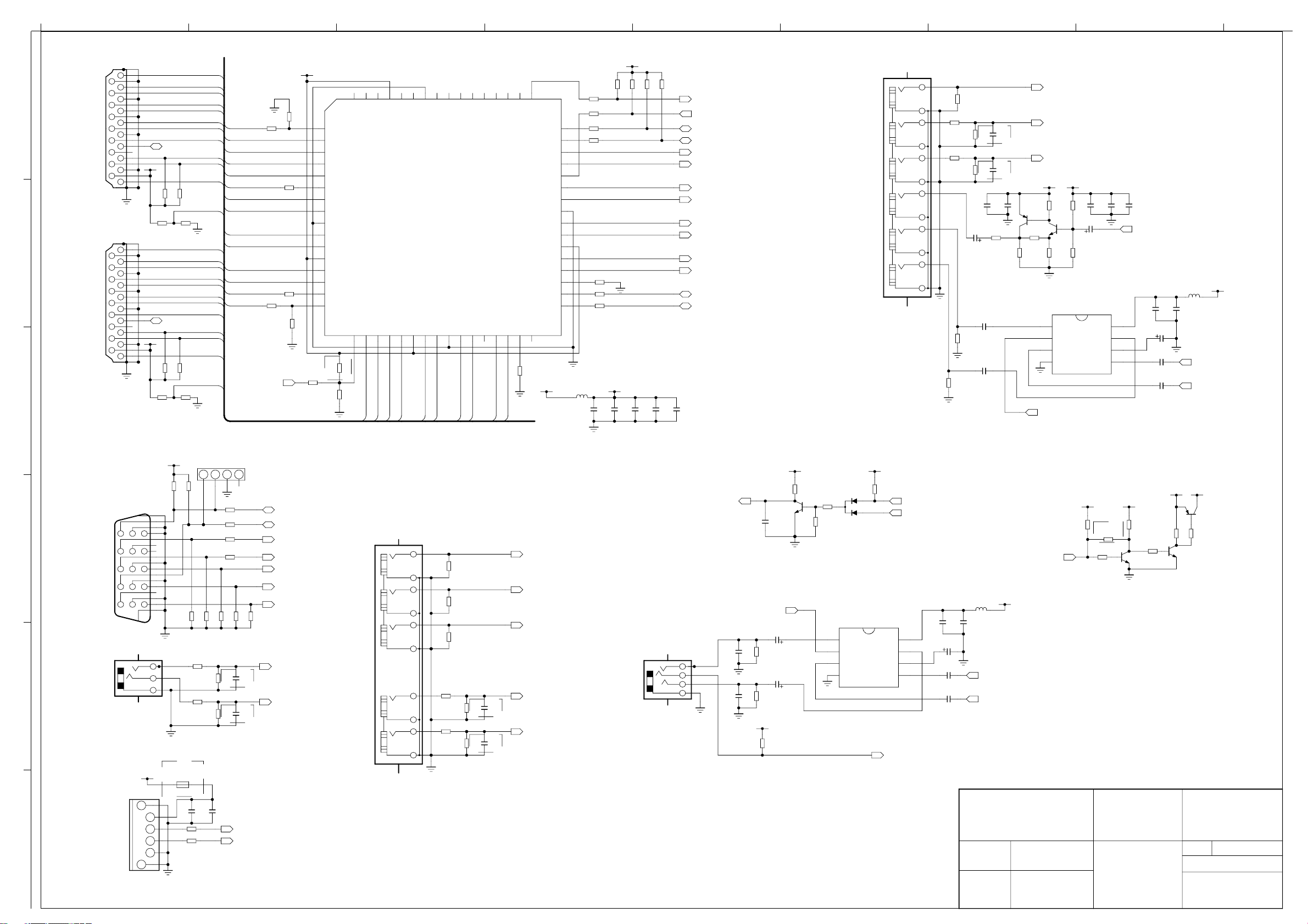
ABCDEFGH
R243
22
R244
0
R245
22
22
R246
6.3V
3.3V_HDMI
4.7K
R250
0
0
0
3.3V_HDMI
10u
16V
100n
C207
4.7K
R251
C208
16V
4.7K
R252
100n
C209
R253
16V
4.7K
100n
C210
16V
100n
C211
HDMI_EN
001:E5
HDMI_HPD 001:A2
001:A3
HDMI_SDA
001:A3
HDMI_SCL
HDMI_RXC-
HDMI_RXC+
HDMI_RX0-
HDMI_RX0+
HDMI_RX1-
HDMI_RX1+
HDMI_RX2-
HDMI_RX2+
TUNER_SCL
TUNER_SDA
001:A2
001:A2
001:A2
001:A2
001:A3
001:A3
001:A3
001:A3
001:E3;004:B4;004:F4
001:E3;004:B4;004:F4
Y1R2
W1
AVAV OUT
R1
Y2
W2
AV13-06-526
X209
R274
R271
10K
R272
10K
75
100K
R273
R276
R277
R275
100K
12K
12K
16V
470u
C222
C223
C220
2.2u
25V
C221
2.2u
25V
C224
C225
10u
470p
470p
16V
R278
75
NC
50V
NC
50V
C226
100n
V206
BC857AW
R288
220
820
R279
001:A3
AV_V
AV_L 001:A4
001:A4
AV_R
12V
R291
R297
1.5K
V211
BC847AW
220
R292
R298
1
OUT1
2
MUTE
3
IN1
4
GND
MUTE_BH3547
5V
1u
33K
10V
C232
16V
220u
C231
120K
N203
BH3547F
VCC
OUT2
BIAS
IN2
002:E4;002:F4
100n
C233
8
7
6
5
10u
C237
10V
AVOUT_V
001:A3
16V
C229
47u
25V
C230
1u
10V
C228
1u
10V
100n
C235
120ohm
10u
6.3V
L203
3A
C234
AVOUT_R
AVOUT_L
5V_BH3547
001:A4
001:A4
R226
1K
R227
1K
3.3V_HDMI
R228
33K
R229
33K
1M
R231
1M
R230
R232
100
10
11
12
13
14
15
16
1
2
3
4
5
6
7
8
9
54
55
56
57
58
59
60
61
62
63
64
NC
CRX2P
BHPD
BSDA
BSCL
BRXCM
BRXCP
BPWR5V
BRX0M
BRX0P
VSS
BRX1M
BRX1P
VCC12
BRX2M
BRX2P
APWR5V
AHPD
RESET18ASDA19ASCL20ARXCM21ARXCP22VCC_2223ARX0M24ARX0P25VSS_2526ARX1M27ARX1P28NC_2829ARX2M30ARX2P31REXT32NC_32
17
NC
R234
4.7K
10K
R233
HDMI1_SDA
CRX2M
VCC_61
HDMI1_SCL
HDMI1_RXC-
CRX1P
HDMI1_RXC+
CRX1M
VSS_58
HDMI1_RX0-
CRX0P
IT6633E-P
HDMI1_RX0+
CRX0M
CPWR5V
N201
HDMI1_RX1-
CRXCP
HDMI1_RX1+
52
53
CSCL
CRXCM
HDMI1_RX2-
50
51
CHPD
CSDA
499
R242
HDMI1_RX2+
49
TXPWR5V
TXSDA
TXSCL
TXCM
TXCP
TXHPD
TX0M
TX0P
VSS_41
TX1M
TX1P
VCC_38
TX2M
TX2P
PCADR0
PCSCL
PCSDA
1%
3.3V_AMP
48
47
46
45
44
43
42
41
40
39
38
37
36
35
34
33
120ohm
L201
R247
R248
R249
3A
001:A2;002:A2
CEC
4.7K
4.7K
R208
R206
3K
001:A2;002:A1
CEC
4.7K
4.7K
R209
R207
3K
HDMI2_RX2+
HDMI2_RX2HDMI2_RX1+
HDMI2_RX1HDMI2_RX0+
HDMI2_RX0HDMI2_RXC+
HDMI2_RXC-
HDMI2_SCL
HDMI2_SDA
HDMI2_HPD
HDMI2_BPWR5V
HDMI1_RX2+
HDMI1_RX2HDMI1_RX1+
HDMI1_RX1HDMI1_RX0+
HDMI1_RX0HDMI1_RXC+
HDMI1_RXC-
HDMI1_SCL
HDMI1_SDA
HDMI1_HPD
HDMI1_APWR5V
HDMI2_HPD
HDMI2_SDA
HDMI2_SCL
HDMI2_RXC-
HDMI2_RXC+
HDMI2_BPWR5V
HDMI2_RX0-
HDMI2_RX0+
HDMI2_RX1-
HDMI2_RX1+
HDMI2_RX2-
HDMI2_RX2+
HDMI1_APWR5V
HDMI1_HPD
HDMI_RESET
001:E5
1
2
3
4
5
1
2
6
8
9
10
11
12
HDMI2HDMI1
13
14
15
16
17 7
18
19
HDMI
X202
1
2
3
4
5
6
8
9
10
11
12
13
14
15
16
17 7
18
19
HDMI
X201
HDMI2_5V
R203
R201
1.5K
HDMI1_5V
R204
R202
1.5K
3
5V_STB
TXD
4
R205
R210
4.7K
4.7K
5
10
15
4
VGAVGA AUDIO
5
6
89
234
12 13 14
5289000155 & 5986A00911
HC1038-15F-3.08
USB
1
67
11
X203
L
R
G
JY-3541L-01-030
X204
5V_USB
GG
1
X205
2
34
UBA-100/W
53131000H0
FU201
SMD1206P075TF
750mA
R214
R215
R213
10u
C201
22K
R211
10K
R212
10K
R216
10V
5.1
5.1
22K
100n
GND
RXD
3
2
R219
100
R220
100
R221
100
R222
100
R22375R22475R225
12K
R217
C203
470p
12K
R218
C204
470p
C202
USB_D-
USB_D+
NC
1
50V
50V
75
NC
NC
X206
001:E3
001:E3
NC
VGA_SCL_RXD
VGA_SDA_TXD
001:A3
VGA_VS
VGA_HS 001:A3
001:A3
VGA_B+
VGA_G+
001:A3
VGA_R+
001:A3
001:A4
VGA_L
VGA_R 001:A4
001:E3
001:E3
X207
HJR-613/PB-3
YPBPR
5V
10K
R257
002:F4;002:G3
001:A3
YPBPR_Y
G1
B1
R1
W2
R2
R237
R238
R239
R235
10K
R236
10K
75
YPBPR_PB
001:A3
75
001:A3
YPBPR_PR
75
001:A4
12K
R240
12K
R241
C205
470p
C206
470p
50V
50V
YPBPR_L
NC
001:A4
YPBPR_R
NC
HP OUT
ST-113
X208
L
G2
R
G5
MUTE_BH3547
002:E4;002:G3
C212
C213
100n
100n
1u
10V
MUTE_BH3547
10V
100u
1K
C214
R254
10V
100u
1K
C215
R255
3.3V
10K
R256
V201
BC847AW
C236
R258
10K
47K
R259
1
2
3
4
52302B1531
D201
MMBD1204
N202
BH3547F
OUT1
MUTE
IN1
GND
3.3V
R267
4.7K
VCC
OUT2
BIAS
IN2
HP_DETE
MUTE_PHOUT
POWEROFF_MUTE
8
7
6
5
001:E3
001:E4
004:E2
16V
C216
47u
25V
C219
1u
10V
C217
1u
10V
100n
C227
120ohm
10u
6.3V
L202
3A
C218
HPOUT_R
HPOUT_L
5V_BH3547
001:A4
001:A4
5V 5V_BH3547
3.3V 3.3V_STB
NC
4.7K
R266
R260
0
R261
EOP_PWON001:E3
1K
R264
4.7K
V202
BC847AW
R262
1K
10K
R265
V203
BC847AW
1K
R263
BC857AW
V204
TITLE: DWG NO.
INTERFACE 9232ME7001DL
DRAWN BY
APPROVED BY
REV.
Sheet to
XIAMEN OVERSEAS CHINESE
ELECTRONIC CO., LTD.
A1.0
2
XOCECO
4
Page 38
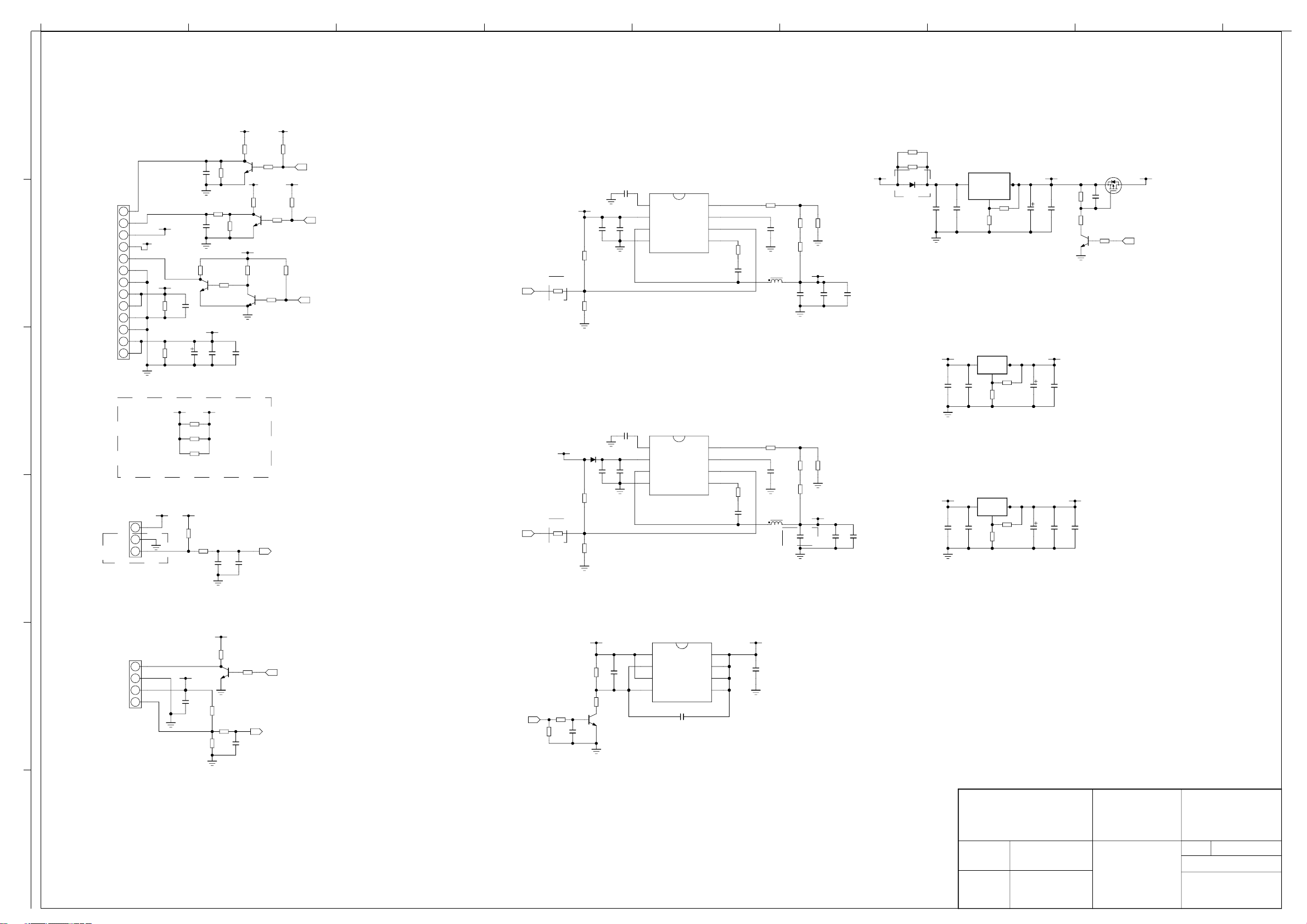
ABCDEFGH
1
5V_STB
5V
R359
1K
R320
V304
BC847AW
1u
47K
R315
C303
BL_ON
13
PWM
12
5V_STB
11
5V
10
2
POWER_ON
GND
GND
12V
12V
GND
GND
12V_AMP
12V_AMP
TJC3S-13A
X301
5283100024 BBY
PWM wave: C304=NC,R311=0
5V_STB
5V
9
8
7
12V
6
5
4
3
2
1
47K
47K
R301
R302
BC847AW
3
LCD panel size less than 37",mount R306,R307,R308
3.3V_STB
5V_STB
X302
5V_STB
1
2
GND
3
4
KEY
R311
1u
C304
1K
R310
V302
1u
16V
C343
12V_AMP
35V
C302
470u
12V_AMP12V
R306
0
R307
0
R308
0
R303 change to 5.6K when use touch key
4.7K
R303
R305
1K
10K
R316
1K
100n
2K
R318
BC847AW
C306
10n
C305
R321
V305
BC847AW
5V_STB
4.7K
R322
V306
1u
16V
10n
5V
1K
C344
C307
R323
10K
R325
10K
R324
4.7K
KEY
4.7K
R326
R328
BL_ON
001:E3
5V_STB
4.7K
R327
001:E3;001:G5
PWM
4.7K
POWER_ON 001:E3;003:D2;003:D4;003:H2
001:E2
001:E3;003:B2;003:D4;003:H2
001:E3;003:B2;003:D2;003:H2
POWER_ON
POWER_ON
NC
R330
0
NC
R331
0
12V
12V
16V
R333
100K
33K
R334
D301
B140-13-F
16V
R335
100K
33K
R336
C310
C311
10u
10u
N301
MP1496
1
SS
2
IN
3
SW
4
GND
Vout=0.8*[1+(R343+R344)/R347]
N302
MP1496
1
SS
2
IN
3
SW
4
GND
Vout=0.8*[1+(R345+R346)/R348]
16V
16V
50V
10n
C315
50V
10n
C316
10u
10u
C313
C314
FB
VCC
EN/SYNC
BST
FB
VCC
EN/SYNC
BST
5V_STB
0
R339
R341
200K
16V
100n
C321
47K
R343
0
R344
75K
R347
8
7
6
5
1.3V 650mA
L301
16V
C318
100n
NR6045T4R5M
0
R340
R342
75K
16V
100n
8
7
6
5
C322
C323
R345
R346
22u
47K
6.8K
6.3V
R348
1.2V
C325
10K
1u
10V
16V
C327
100n
5.10V
C324
22u
5V_USB
NC
6.3V
16V
C326
10u
16V
10u
C328
C319
100n
16V
L302
NR6045T4R5M
0
R358
0
D302
B240-13-F
NC
N304
AZ1084S-ADJ
OUT
IN
ADJ
10V
10u
C332
C329
100n
Vout=1.25*(1+R349/R352)
5V 2.5V
10V
10u
C333
100n
C330
Vout=1.25*(1+R350/R353)
5V
10V
10u
C334
100n
C331
Vout=1.25*(1+R442/R354)
215
R352
365
R349
N305
AP1117-ADJ
IN OUT
R353
442
R350
N306
AP1117-ADJ
IN OUT
R354
442
R351
442
909
3.37V 150mA
3.3V_STB
16V
220u
C335
16V
220u
C336
16V
220u
C337
47K
R355
100n
C338
4.7K
R356
V308
BC847AW
2.5V 150mA
100n
C339
1.8V_DDR2
10V
100n
C340
AO3401A
S
1u
10V
C342
R357
4.7K
1.86V 200mA
10u
C341
V309
3.3V
D
G
001:E3;003:B2;003:D2;003:D4
POWER_ON
1
2
3
4
S2
G2
S1
G1
5270603001
N303
AO4803A
C317
100n
50V
5V_STB
X303
LED
1
GND
IRR
2
3
4
IR_POWER
5
5V_STB
100n
BC847AW
V303
C301
2.2K
R314
100
4.7K
R312
R313
220
R317
50V
R319
4.7K
22p
C308
IRIN
LED
001:E3
001:E2
001:E3
PANEL_ON
R332
4.7K
4.7K
R329
12V
1u
47K
16V
R337
C312
R338
4.7K
V307
BC847AW
1u
C309
D2_8
D2_7
D1_6
D1_5
FOR 12V PANEL
VCC_PANEL
8
7
6
5
100n
C320
TITLE: DWG NO.
POWER&CONNECTOR 9232ME7001DL
6
DRAWN BY
APPROVED BY
REV.
Sheet to
4
A1.0
4
XOCECO
XIAMEN OVERSEAS CHINESE
ELECTRONIC CO., LTD.
Page 39
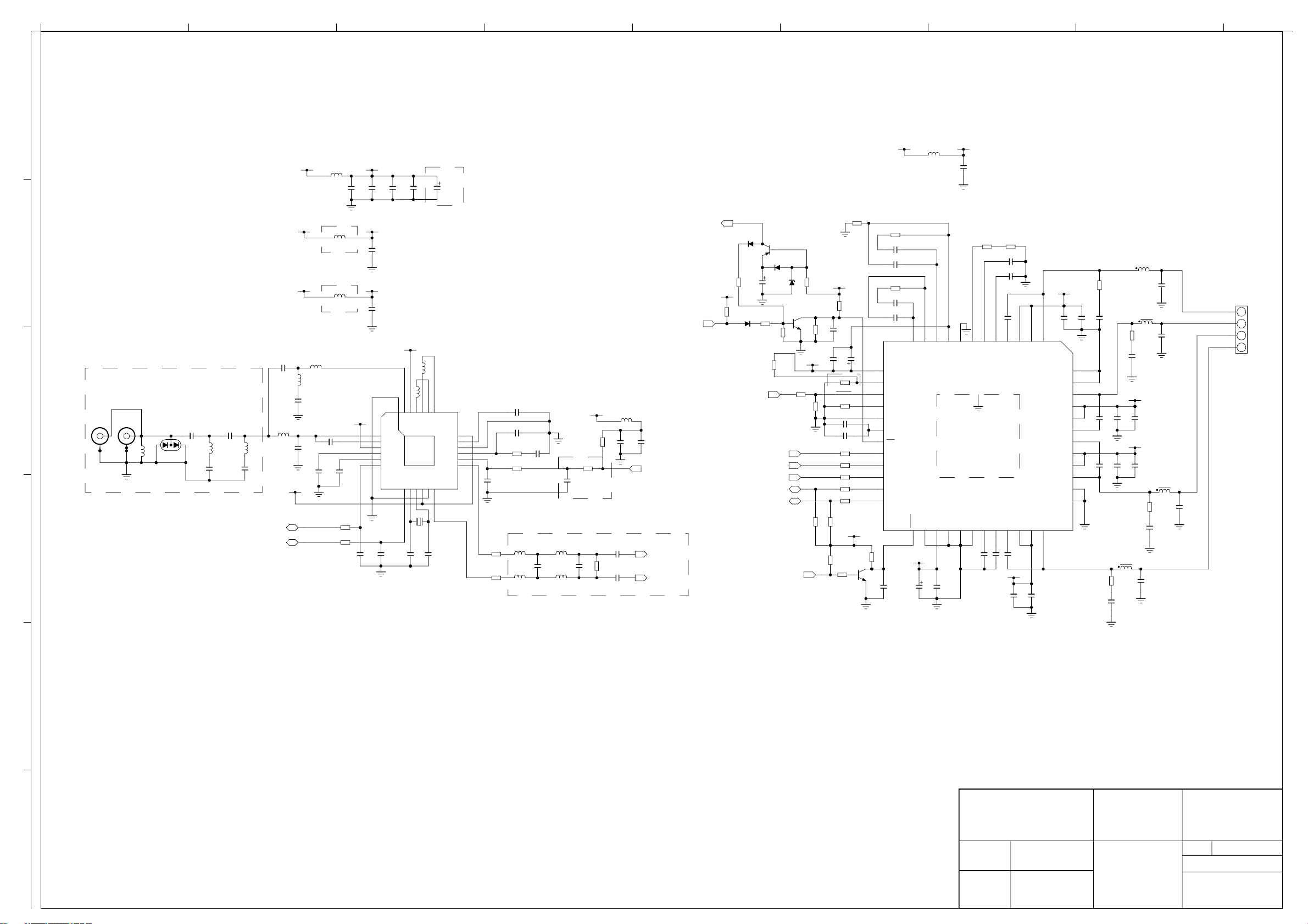
ABCDEFGH
1
L411
3.3V 3.3V_AMP
120ohm
3A
L407
3.3V
120ohm
3.3V_TUNER
2
3.3V_TUNER
C405
4.7p
ADD NOTCH FILTER C401=68pF,C403=47pF
L402=220nH,L403=220nH,C402=120pF,C404=150pF
NOT ADD NOTCH FILTER C401=10nF,C403=10nF
3
GND
L402=NC,L403=NC,C402=NC,C404=NC
@pinCo1@pinCo
@pinCo
@pinCo1@pinCo
X403
X401
IF-10S
NF-12
GND
NC
180nH
L401
LBAV99LT1G
D401
C401
68p
50V
C403
47p
50V
L402
220nH
50V
120p
C402
001:E3;002:E2;004:F4
001:E3;002:E2;004:F4
50V
L403
220nH
150p
C404
TUNER_SCL
TUNER_SDA
47nH
50V
22nH
50V
L404
50V
3.3V_TUNER
8.2nH
L405
1n
4.7p
L406
C406
C407
16V
4
3A
10u
C411
L416
15nH
531A3A51H0
L417
15nH
531A3000H0
3.3V_RFB
50V
10p
C409
1u
16V
100n
C408
R403
33
R404
33
3.3V_TUNER
6.3V
C413
100n
3.3V_RFA
10n
C419
3.3V_RFB
10n
C417
C410
39p
50V
1
2
3
4
5
6
C412
16V
50V
50V
50V
C415
100n
RF_2
Open_D
VCC3
Det1
Det2
SCL
39p
C414
1u
16V
C470
3.3V_RFA
150nH
24
25
GND
RF_1
VCC23
SDA
Xtal_l
7
G401
16MHz
33p
C416
10V
150nH
22
23
TF1n
TF1p
R620D
VCC10
Xtal_O
8
9
50V
L408
21
TF2p
N401
DVSS
10
50V
16V
L409
19
20
TF2n
VCC18
VDD_PLL
AVSS
IF_AGC
IF_P
IF_N
12
11
33p
C418
220u
CP
NC
C469
10u
6.3V
C442
R433
12V
10K
R432
C430
100n
100n
10K
NC
R425
R426
18.2K
C432
4.7u
100n
C433
R427 47
R428
R429
R430
R431 47
4.7K
R402
4.7K
R423
R424
4.7K
0
16V
C431
47
47
47
3.3V_AMP
BC847AW
V403
10u
R434
C434
4.7K
13
14
15
16
17
18
19
20
21
22
23
24
C435
100n
R435
470
C436
47n
C437
4.7n
R436
470
C438
47n
C439
4.7n
10
11
12
VR_ANA
PLL_FLTM
AVDD
A_SEL
MCLK
OSC_RES
DVSSO
VR_DIG
PDN
LRCLK
SCLK
SDIN
SDA
SCL
PLL_FLTP
RESET26STEST27DVDD28DVSS29GND30AGND31VREG32GVDD+OUT33BST_D34PVDD_D_3435PVDD_D3_536OUT_D
25
3.3V_AMP
16V
10u
C440
C441
100n
9
AVSS
GND_49
8
PBTL
TAS5711
N402
R437
100
7
OC_ADJ
SSTIMER
49
C443
100n
6
C444
R438
22K
C445
2.2n
C446
1u
39n
C447
4
5
BST_A
GVDD_OUT
1u
39n
12V_AMP
C449
100n
3
PVDD_A_2
PVDD_A_3
C448
1n
C450
12V_AMP
C451
100n
1
2
OUT_A
PGND_AB_48
PGND_AB_47
OUT_B
PVDD_B_45
PVDD_B_44
BST_B
BST_C
PVDD_C_41
PVDD_C_40
OUT_C
PGND_CD_38
PGND_CD_37
1n
C452
48
47
46
45
44
43
42
41
40
39
38
37
R439
C453
330p
39n
C454
39n
C455
18
R441
C459
12V_AMP
C457
100n
12V_AMP
C458
100n
L412
NR8040T220M
18
R440
C456
330p
L413
NR8040T220M
L414
NR8040T220M
18
330p
1n
C460
1n
C461
NR8040T220M
18
R442
C463
330p
1u
C462
1u
C464
1u
C465
L415
1u
C466
X402
1
L+
2
L-
3
R-
4
R+
5283040024 BBY
POWEROFF_MUTE002:F4
AMP_STB
001:E2
C421
100n
16V
C422
16V
R405
100
R406
100
C420
100n
330p
50V
R407
1.8K
R408
100
L418
1uH
L419
1uH
C423
6.8n
50V
50V
16V
L420
2.2uH
L421
56p
C467
2.2uH
CLOSE TO 6M182
R410
10K
22n
C426
CLOSE TO 6M182
33p
50V
18
17
16
15
14
13
5V
C468
10K
R411
120ohm
C427
C424
100n
16V
C425
510
R419
100n
16V
L410
100n
3A
16V
C428
2.2u
AGC
10V
VIFP
VIFM
001:B5
001:E3;002:E2;004:B4
001:B5
001:B5
3.3V_AMP
4.7K
R412
D403
LL4148
BC857AW
2.2K
D402
LL4148
001:E4
V401
R413
MCLK
001:E4
001:E4
001:E4
001:E4
D404
LL4148
16V
220u
C429
R414
2.2K
R416
LRCLK
SCLK
SDIN
TUNER_SDA001:E3;002:E2;004:B4
TUNER_SCL
AMP_RESET
D405
BZV55-B9V1
BC847AW
V402
10K
R415
4.7K
R417
1K
R418
4.3K
R420
3.3V_AMP
0
10K
R421
4.7K
R401
5
TITLE: DWG NO.
TUNER& 9232ME7001DL
6
DRAWN BY
APPROVED BY
REV.
Sheet to
4
A1.0
4
XOCECO
XIAMEN OVERSEAS CHINESE
ELECTRONIC CO., LTD.
Page 40
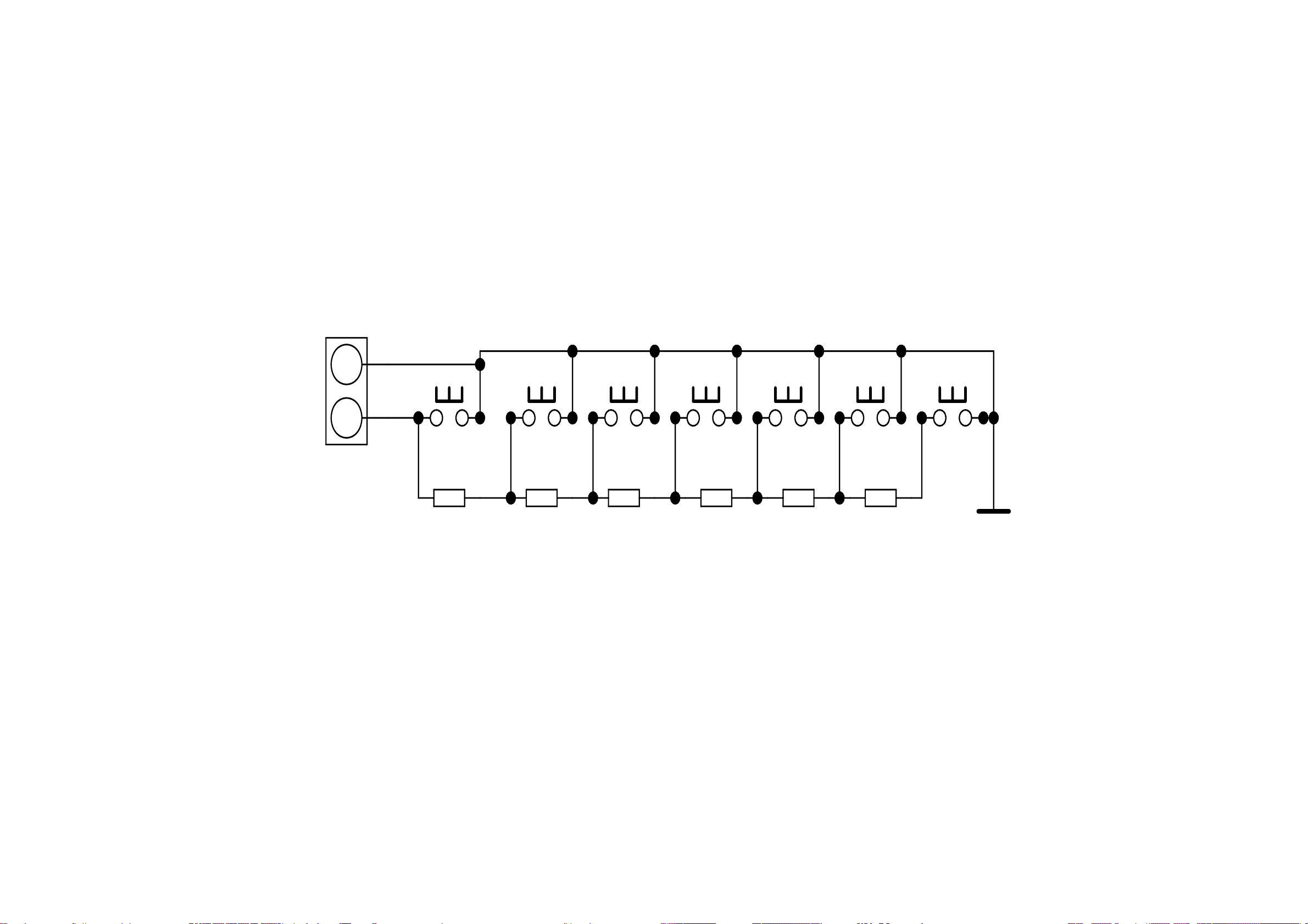
X901
POWER SOURCE MENU VOL-VOL+ CH+ CH-
1
2
S907 S906 S905 S903 S904 S901 S902
R906
1K
R905
1K
R904
1.5K
R903
2.4K
R902
4.3K
R901
10K
Key board
Page 41
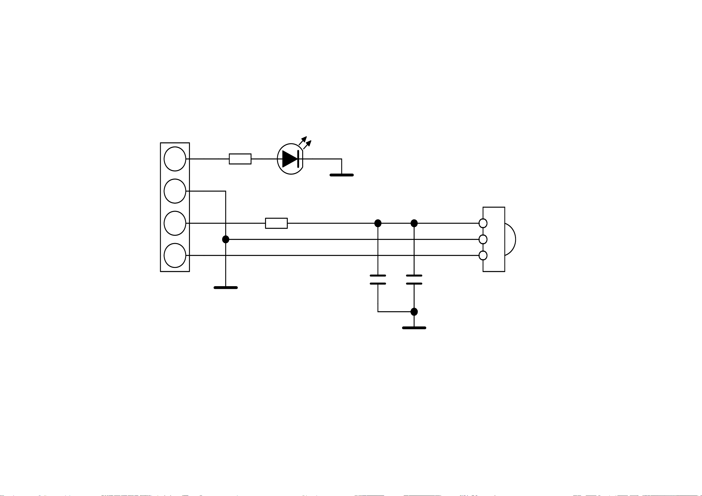
LED1
GPR2503/P322
X911
1
2
3
4
R911
120
R913
47
C911
100n
HRM538BB5117
N911
Vcc
GND
Vout
10u
C912
IR board
Page 42
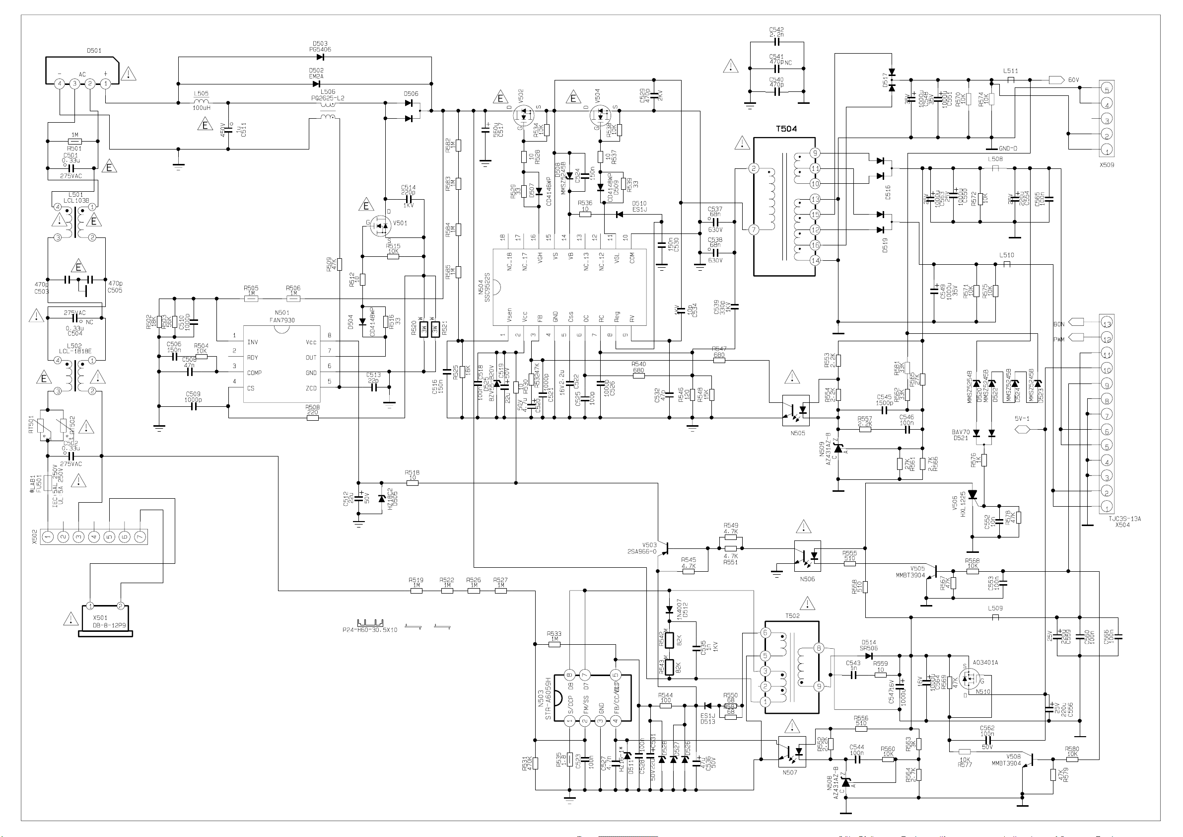
Power board
Page 43
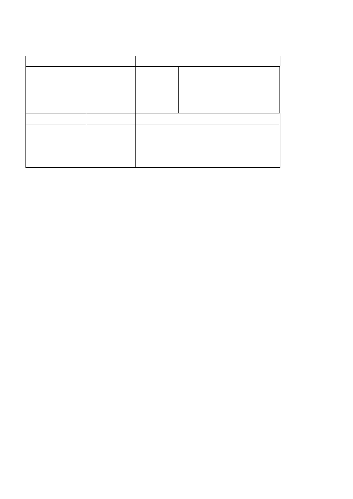
APPENDIX-A: Main assembly 9232ME7711 LCE-32R77
NAME NO. MAIN COMPONENT AND IT'S NO.
Main processing
board
IR board
Key board
Power board
Remote control
Panel assembly
N101
N401
XI6ME01001A0
XI635ME00200
XI635ME00501
XI6ME01020A0
XI6011301001 RC-1310-0A
XI6379000400 HV320WX2-200X
N102
N402
N201
MST6E182VGC (5270182003)
R620D (5270620002)
EN25Q32B-104HIP (5272532007)
TAS5707 (5275707001)
IT6633E-P(5276633001)
Page 44
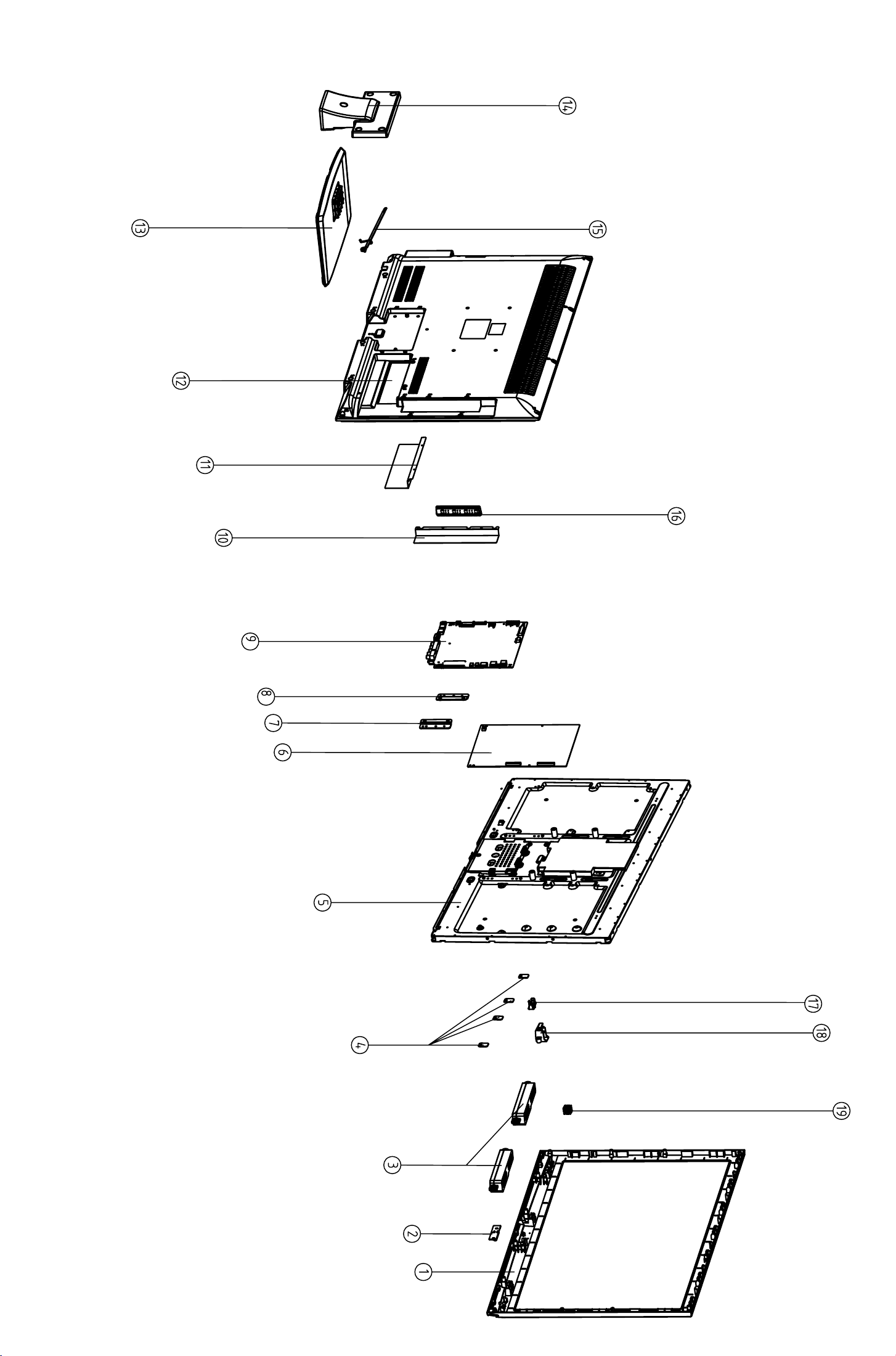
APPENDIX-B: Exploded view (LCE-32R77)
Page 45
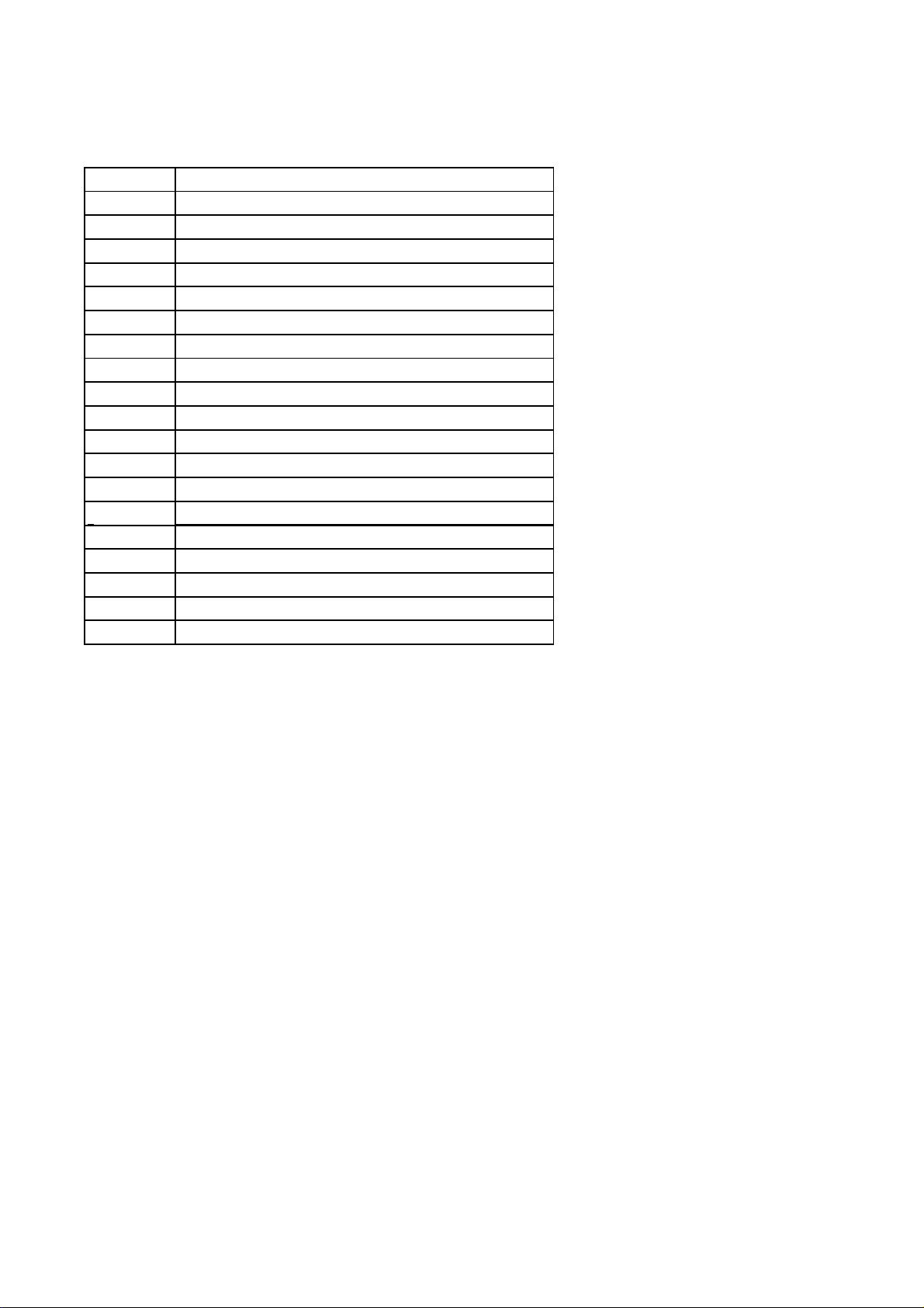
PART LIST OF EXPLODED VIEW
REF.No. DESCRIPION
1 Front cabinet assembly
2
3
4 Panel pressing block
5
6 Power board assembly
7
8
9
10 Interface baffle (right)
11 Interface baffle (down)
12 Back cover assembly
13
14
15
16
17
18
19
IR assembly
Sound box assembly
Display panel
Standing pole bracket (right)
Standing pole bracket (left)
Main board assembly
Pedestal faceplate assembly
Pedestal standing pole
Adjustalbe clasp
Key board assembly
3D light guided pole
Power cord bracket
Power cord clip
Note: Design and specification are subject to change without notice.
Page 46
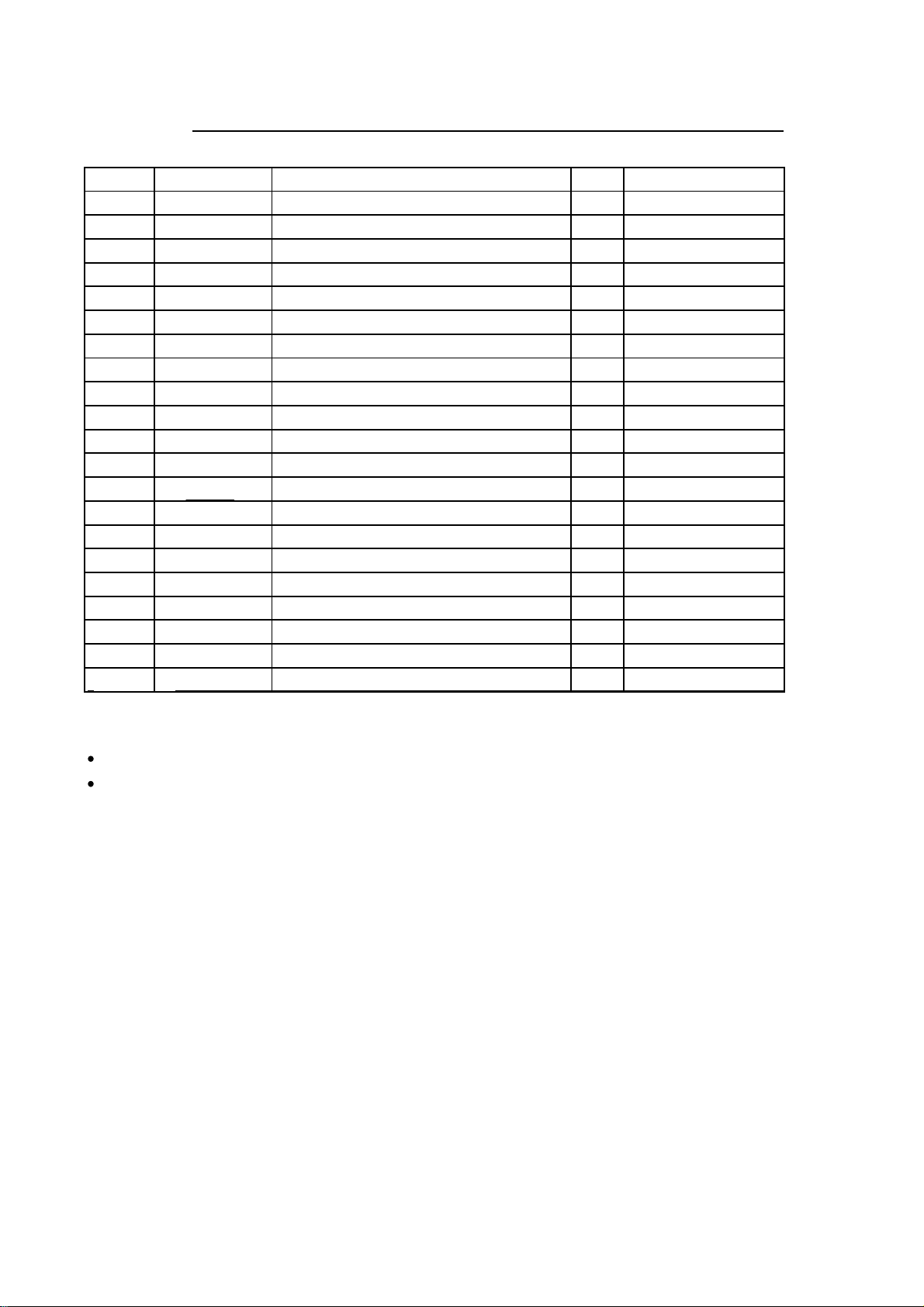
PART LIST
LCE-32R77 ver.1.0
REF.No. PARTS No. DESCRIPION Q'TY REMARK
1
2
3
4
5
6
7
8
9
10
11
12
13
14
15
16
17
18
19
20
21
XI6632770080
XI635ME00200
XI6170899A00
XI5810080700
XI6379000400
XI6ME01020A0
X5810A78800
XI5810A78700
XI6ME01001A0
XI5810L78510
XI5810R78610
XI673277H090
XI6150110010
XI58D0030710
XI5720124000
XI635ME00501
XI570032001B
XI58B0A45610
XI572011201C
XI6011301001
XI5944040410
Front cabinet assembly 1
IR assembly
Sound box assembly
Panel pressing block 4
Display panel
Power board assembly 1
Standing pole bracket (right)
Standing pole bracket (left)
Main board assembly
Interface baffle (right) 1
Interface baffle (down) 1
Back cover assembly 1
Pedestal faceplate assembly
Pedestal standing pole
Adjustalbe clasp
Key board assembly
3D light guided pole
Power cord bracket
Power cord clip
Remote control
User manual
1
1
1 HV320WX2-200X
1
1
1
1
1
1
1
1
1
1
1
1
Only the parts in above list are used for repairing.
Other parts except the above parts can't be supplied.
Page 47
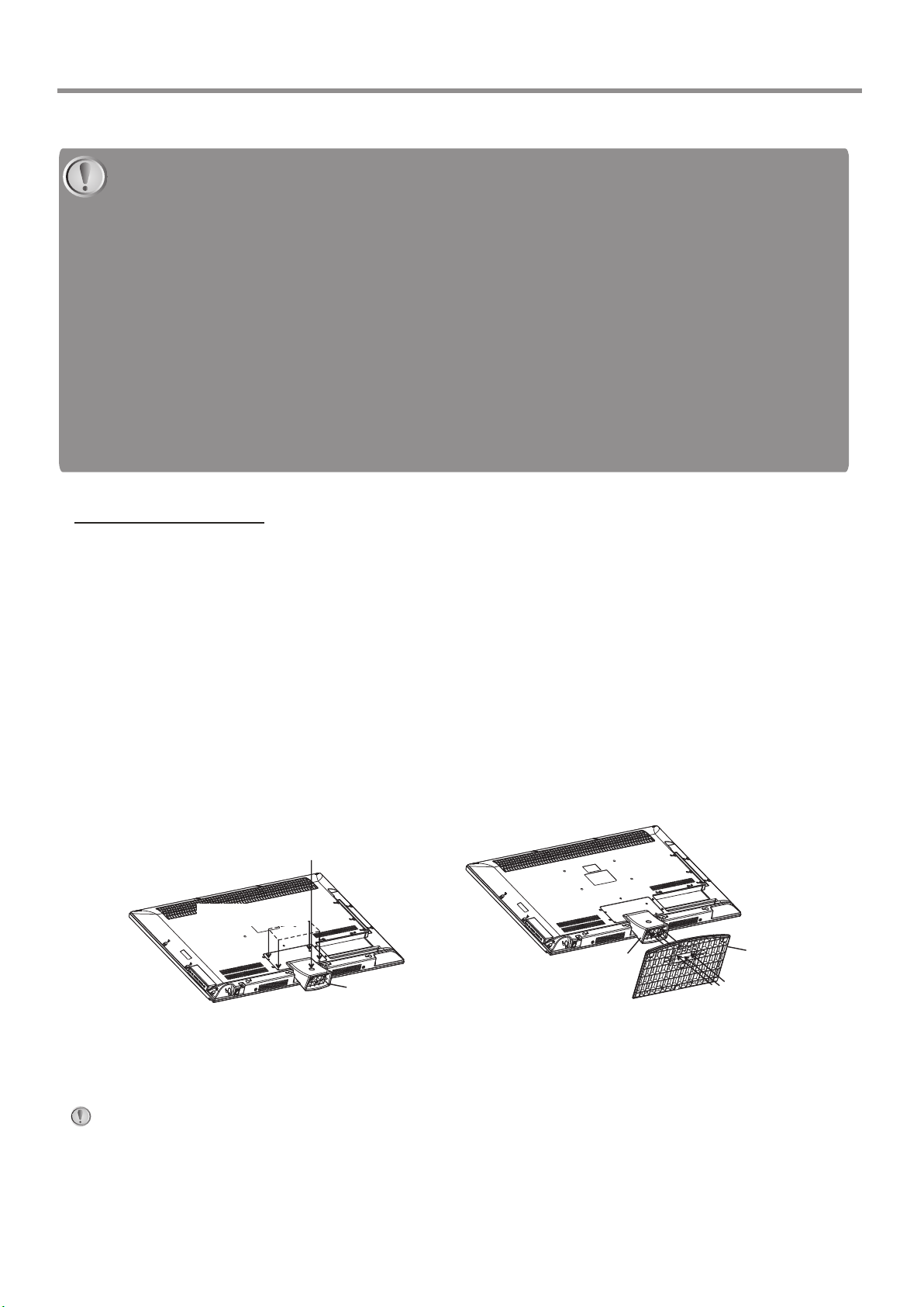
Appendix: Installing the Stand
If the stand is provided, please read these instructions thoroughly before attempting this installation.
Safety Precautions:
1.Please read these instructions thoroughly prior to attempting this installation.
2.Be sure to handle this product very carefully when attempting assembly. If you are unsure of your
capability, or the use of tools necessary to complete this activity, refer to a professional installer or
service personnel. The manufacturer is not responsible for any damages or injuries that occur due to
mishandling or improper assembly/installation.
3.When using a table or bench as an aid to assembly, be sure to put a soft cushion or covering to prevent
accidental scratching or damage to the unit's finish.
4.The speaker is not intended to support the weight of this display. Do not move or handle this product
from the speaker; which can cause damage to the display not covered under the manufacturer's
warranty.
To install the stand:
1. Remove the stand from the box and place it on a table or bench.
You must pay attention to the direction of the stand. The wide portion of the stand should go towards
the front of the TV.
2. Lay your TV flat (screen down) on the edge of a table or bench. Make sure that you put down a soft
cushion or cloth so that your TV is not scratched.
3. Attach the stand column to the back of the TV, and then secure the stand column to the TV with the
screws provided.
4. Align the stand to the stand column, then secure the stand to the stand column with the screws
provided.
T4 screw
Four M5 screws
Stand
Stand
column
Stand
column
S ecure with
three screws
NOTE:
1.Appearance of this product in illustrations may differ from your actual product, and is for comparative
purposes only.
2.Design of this accessory or display products are subject to change without notice.
Page 48
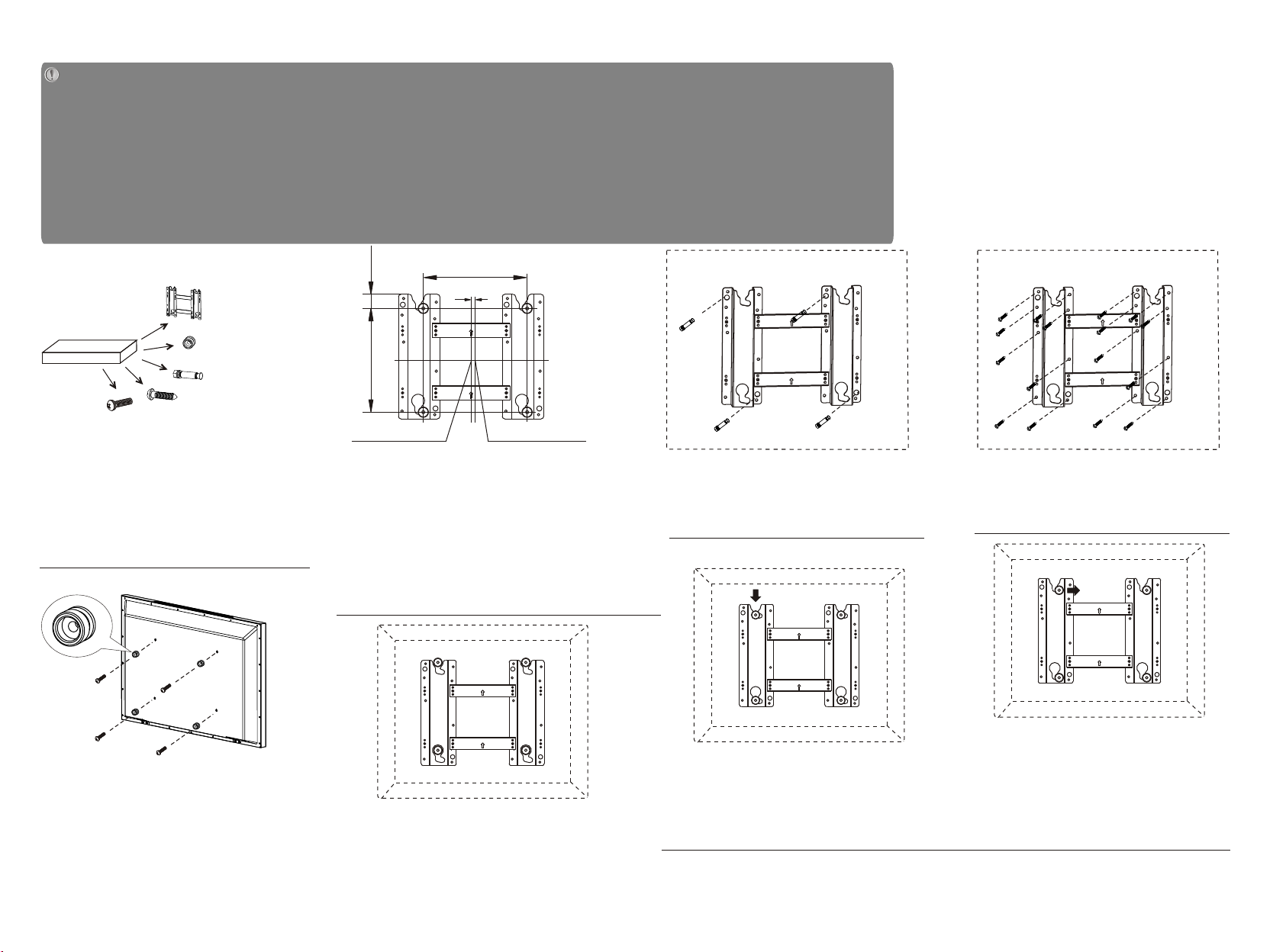
WALL MOUNTING INSTRUCTIONS
Safety Precautions:
1. Be sure to ask an authorized service personnel to carry out setup.
2. Thoroughly read this instruction before setup and follow the steps below precisely.
3.The wall to be mounted should be made from solid materials. Only use accessories supplied by the manufacturer.
4.Very carefully handle the unit during setup. We are not liable for any damage or injury caused by mishandling or improper installation.
5.Be sure to place the unit on a stable and soft platform which is strong enough to support the unit.
6.Do not uplift the speaker when moving the display. The appearance of the unit may different from the actual ones.
7.Design and specifications are subject to change without notice.
8. Retain these instructions for future reference.
Note: All the wall mounting parts are
optional and may be unavailable in
your model.
Below we will show you how to mount the
Display on the wall using our company’s
wall mounting components.
Take out these
parts from the
box
Combination Screw
Fig.1
1. There are three options of wall mounting
ho ld er with different specifications
:200200,200400,200600. Please check your
wall mounting holder for its specification.
Wall Mounting Holder
Wall Mounting Connector
Expansion Bolt
Wood Screw
Wall mounting fix-h ole c ent er
X
8
200 27
Rea r wall mounting hole center
Fig.2
2. Due to the wall mounting fix-groove leaning to the
right side, the whole unit will lean to right side after
installation, please carefully measure the position of
the holes you want to drill, refer to the parameters
on Fig.2 when drilling the holes.
Note: The "X" in Fig.2 represents a data. It may be
200mm or 400mm or 600mm.
(Unit:mm)
Wall
Fig.3 a
3a. Screw 4pcs expansion bolts to fix the
wall mounting holder on the wall.
Wall
Fig.3 b
3b. If your wall is a wooden structure, please
fix the wall mounting holder on the wall
with 16pcs wood screws.
Fig.4
4. Use the 4pcs combination screws to fix
the wall mounting connector to the rear
of the display unit.(Caution:the direction
of the connectors should be strictly
confirm to the diagram illustrated above).
Fig.5
5. Put the back of the display unit close to the wall
mounting holder, insert the four wall mounting
connectors into the four calabash-shaped holes on
the wall mounting holder. (Fig.5)
Fig.6
6. Let the display unit slowly slide down to
the end of the calabash-shaped hole.
(Fig.6)
8. If you want to dismount the unit do the above steps in reverse order.
7. Push rightwards carefully until the wall
mounting connectors fully slide into the
right fix-grooves and be sure the mounting
is secure.
Fig.7
Page 49

April 2012
 Loading...