

Page 1
FILE NO.
SERVICE MANUAL
LED-LCD TV
LCE-32R40HDW
PRODUCT CODE No.
PRODUCT CODE No.
1 682 349 82: PAL/SECAM
NTSC(AV)
REFERENCE No.:SM0915126
Page 2

CONTENTS
Safety precautions………………………………………………………………………..…
Alignment instructions …………………………….…….…………………………………
Instruction of software upgrading & boot burning ....................................................
Working principle analysis of the unit……………………………….………….………….
Block diagram…………………………………..………………………………….…………
IC block diagram………………………………………………………………………..……
Wiring diagram …………………………………………………………………………….
Troubleshooting guide ………………………………………………………………..……
Schematic diagram…………………………………………………………………………
APPENDIX-A: Assembly list
APPENDIX-B: Exploded View
3
5
13
19
20
21
29
30
33
Page 3

Attention: This service manual is only for service personnel to take reference with. Before
servicing please read the following points carefully.
Safety precautions
1. Instructions
Be sure to switch off the power supply before replacing or welding any components or
inserting/plugging in connection wire. Anti static measures must be taken (throughout the entire
production process!):
a) Do not touch here and there by hand at will;
b) Be sure to use anti static electric iron;
c) It’s necessary for the welder to wear anti static gloves.
Please refer to the part list before replacing components that have special safety requirements.
Do not replace with different components with different specs and type at will.
2. LCD servicing precautions
2.1 Screens are different from one model to another and therefore not interchangeable. Be sure to
use the screen of the original model for replacement.
2.2 Do not use any adapter that is not identical with the TV set. Otherwise it will cause fire or
damage to the set.
2.3 Never operate the set or do any installation work in bad environment such as wet bathroom,
laundry, kitchen, or nearby fire source, heating equipment and devices or exposure to sunlight etc.
Otherwise bad effect will result.
2.4 If any foreign substance such as water, liquid, metal slices or other matters happens to fall into
the module, be sure to cut the power off immediately and do not move anything on the module lest
it should cause fire or electric shock due to contact with the high voltage or short circuit.
2.5 Should there be smoke, abnormal smell or sound from the module, please shut the power off
at once. Likewise, if the screen is not working after the power is on or in the course of operation,
the power must be cut off immediately and no more operation is allowed under the same
condition.
2.6 Do not pull out or plug in the connection wire when the module is in operation or just after the
power is off because in this case relatively high voltage still remains in the capacitor of the driving
circuit. Please wait at least one minute before the pulling out or plugging in the connection wire.
2.7 When operating or installing LCD please don’t subject the LCD components to bending,
twisting or extrusion, collision lest mishap should result.
2.8 As most of the circuitry in LCD TV set is composed of CMOS integrated circuits, it’s necessary
to pay attention to anti statics. Before servicing LCD TV make sure to take anti static measure and
ensure full grounding for all the parts that have to be grounded.
2.9 There are lots of connection wires between parts behind the LCD screen. When servicing or
moving the set please take care not to touch or scratch them. Once they are damaged the screen
Page 4
would be unable to work and no way to get it repaired.
If the connection wires, connections or components fixed by the thermotropic glue need to
disengage when service, please soak the thermotropic glue into the alcohol and then pull them
out in case of dagmage.
2.10 Special care must be taken in transporting or handling it. Exquisite shock vibration may lead
to breakage of screen glass or damage to driving circuit. Therefore it must be packed in a strong
case before the transportation or handling.
2.11 For the storage make sure to put it in a place where the environment can be controlled so as
to prevent the temperature and humidity from exceeding the limits as specified in the manual. For
prolonged storage, it is necessary to house it in an anti-moisture bag and put them altogether in
one place. The ambient conditions are tabulated as follows:
Temperature Operation range 0 ~ +50 oC
Storage range -20 ~ +60 oC
Humidity Operation range 20% ~ 85%
Storage range 10% ~ 90%
2.12 Display of a fixed picture for a long time may cause a permanent after-image on the screen,
as commonly called “ghost shadow”. The degree of the after-image varies with the maker of LCD
screen. This phenomenon doesn’t represent failure. This “ghost shadow” may remain in the
picture for a period of time (several minutes). But when operating it please avoid displaying still
picture in high brightness for a long time.
3. Installation precautions
3.1 The front panel of LCD screen is made of glass. When installing it please make sure to put it in
place.
3.2 For service or installation it’s necessary to use specified screw lest it should damage the
screen.
3.3 Be sure to take anti dust measures. Any foreign substance that happens to fall down between
the screen and the glass will affect the receiving and viewing effect
3.4 When dismantling or mounting the protective partition plate that is used for anti vibration and
insulation please take care to keep it in intactness so as to avoid hidden trouble.
3.5 Be sure to protect the cabinet from damage or scratch during service, dismantling or
mounting.
Page 5
Alignment instructions
2 Adjustment equipment
Digital multimeter
Signal generator (54200)
PC (presetting FLASH software)
VG848, VG849 (VGA, YPbPr and HDMI signal generator)
DVD player with HDMI output
White balance apparatus (CA210)
Monitor
3 Adjustment flow
3.1 Test voltage of power supply
3.1.1 According to wiring diagram "9242KC5101JL", connect main board, power board, IR board and
key board correctly, switch on power supply, then press key ‘power’ to turn on the TV set.
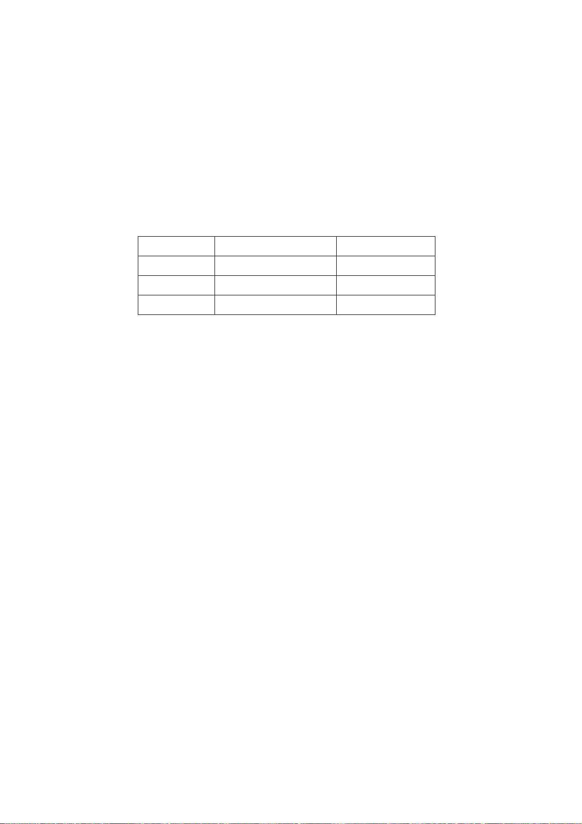
a)Test voltage of socket X302 each pin in turn, please refer to voltage value as Table 1.
Table 1 Voltage of X302 each pin
X302 Pin1 2 3
Vol.
3.3 V~
5.0 V
1.0 V~
3.3 V
0
4、5 6、7
11.5 V~
12.5V
0
b)Test voltage of socket X301 each pin in turn, please refer to voltage value as Table 2.
Table 2 Voltage of X301 each pin
X301
Vol.
Pin1、2 3、4、5
23 V~25 V
8 9 10 11 12 13
31 V~
33 V
4.7 V~
5.3 V
4.7 V~
0
5.3 V
0
3.3 V~
0
5.0 V
Page 6
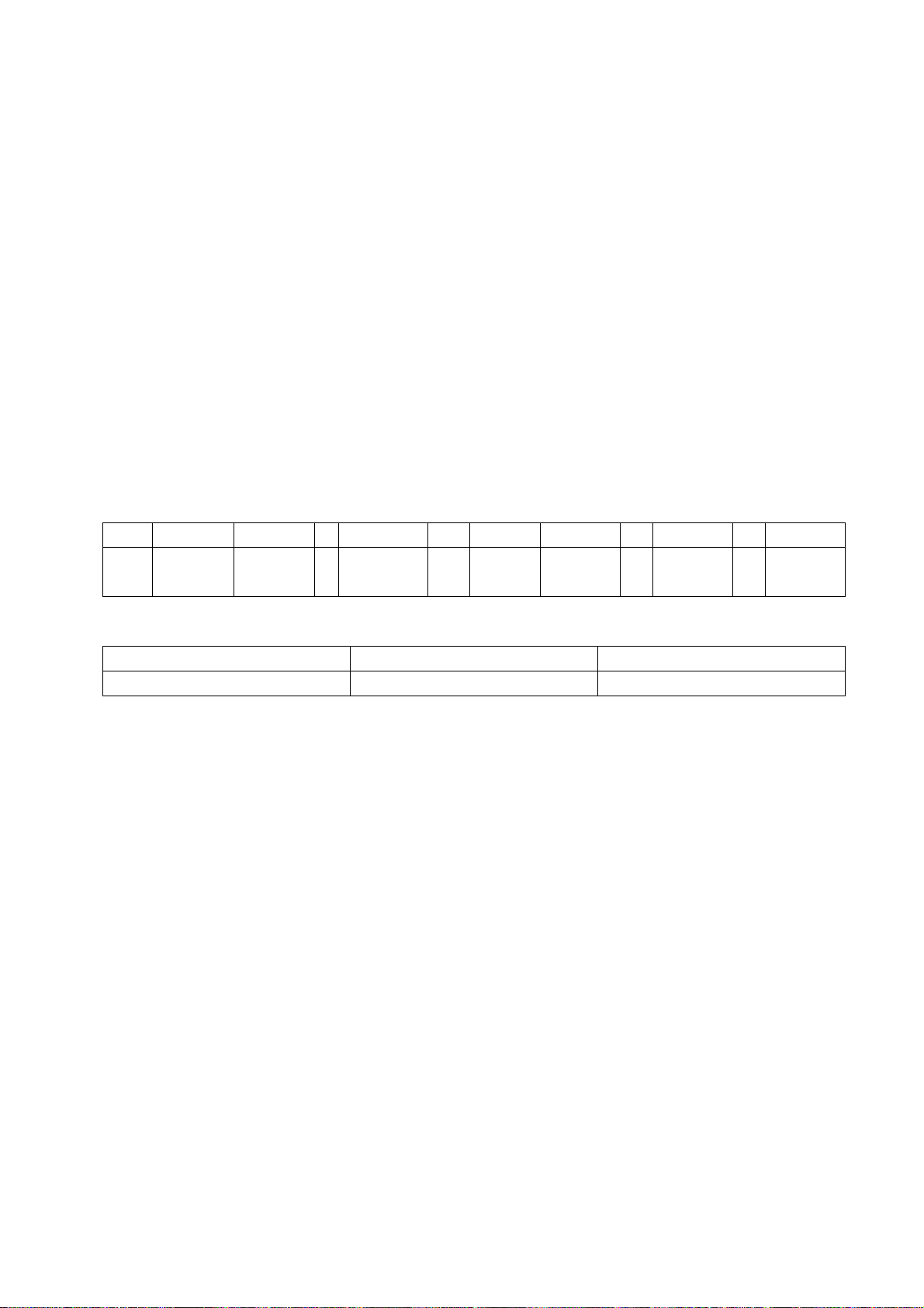
3.2 Adjustment flow chart as Fig.1
Connect to central signal source, check if each function of TV, such
as omitted program, analog parameter control, etc. is normal? Check
if output of earphones, speakers are normal?
Input AV/S-VIDEO signal, check if each function
Input HI definition signal (mode), check if each
Input VGA signal, check if display and each
function, such as analog parameters control, H/V
center, etc., are normal?
Input HDMI signal, check if display and each
function, such as analog parameters control, H/V
Insert U disk, check if functions of MP3 and JPEG
Check if FLASH has been burned
Product main board on line
General assembly and adjustment
White balance adjustment
of both channels are normal?
function of YPbPr is normal?
are normal?
Setting before leaving factory
Check accessories and packing
Fig. 1 Adjustment flow
Page 7

4 Adjustment instruction
4.1 Unit adjustment
4.1.1 According to wiring diagram ‘9242KC5101JL’ , connect main board, power board,
key board and IR board correctly, switch on power supply, check if display is normal?
4.1.2 Instruction of factory menu
a)First press key ‘Program source’, then press number keys “2、5、8、0” in turn to enter initial
factory menu;
b)Press keys “” and “” to move cursor to each adjustment page of initial factory menu, then
press “” to enter into its adjustment menu;
c)Press keys “” and “” to move cursor upwards or downwards within any adjustment page;
d)Press keys “” and “” to adjust any item when cursor is moved onto it;
e)Press key “Menu” to exit to initial menu from any adjustment page;
f)Press key “Exit” to exit from factory menu in any case;
g)Set item “Aging Mode” as “On” to enter into factory aging mode.
4.2 White balance adjustment
4.2.1 Before adjustment
The unit should be working for above 30 minutes to be in stabler state; Use apparatus CA210 to
adjust white balance;
For model of which dimension is bigger than 26”, only 9300K color temperature (that is “normal”)
is needed adjustment, To guarantee BBY test requirements to be met when color temperature are
12000K and 6500K, make sure that chromaticity coordinates of bright scale are (X=285±5, Y=293±8)
and chromaticity coordinates of dark scale are (X=285±8, Y=293±12);
For model of which dimension is 26” or smaller than 26”, only 8000K color temperature (that is
“normal”) is needed adjustment, To guarantee test requirements to be met when color temperature
are 9300K and 6500K, make sure that chromaticity coordinates of bright scale are X=295±5,
Y=305±8) and chromaticity coordinates of dark scale are (X=295±8, Y=305±12);
4.2.2 White balance adjustment of HDMI channel
Input 16-grey-scale signal with format of 800×600/60 Hz (VG848: Timing is 854,PAT is 921),
enter into submenu “color temperature adjustment” of factory menu;
For model of which dimension is bigger than 26”, select “normal” color temperature (that is
9300K), fix item “G Offset”, adjust items “R Offset, B Offset” to set chromaticity coordinates of the 3
rd
scale as (285±8, 293±12)and guarantee luminance within the range of 3 nit to 5 nit; fix item “G
GAIN”, adjust items “R GAIN, B GAIN” to set chromaticity coordinates of the reverse 3
rd
scale as
(285±8, 293±12); adjust items “R Offset, B Offset” and “R GAIN, B GAIN” repeatedly until
chromaticity coordinates of both scales are all (285, 293);
For model of which dimension is 26” and small than 26”, select “normal” color temperature (that is
8000K), fix item “G Offset”, adjust items “R Offset, B Offset” to set chromaticity coordinates of the 3
rd
scale as (295±8, 305±12)and guarantee luminance within the range of 3 nit to 5 nit; fix item “G
GAIN”, adjust items “R GAIN, B GAIN” to set chromaticity coordinates of the reverse 3
rd
scale as
(295±5, 305±8) ; adjust items “R Offset, B Offset” and “R GAIN, B GAIN” repeatedly until
chromaticity coordinates of both scales are all (295, 305);
Set item “ALL COLOR” as “ON” after completing adjustment.
Page 8

4.2.3 White balance adjustment of YPbPr channel
ADC calibration of SD mode: Input color-bar signal with format of 480i/60 Hz (VG848: Timing is
968,PAT is 918), enter into submenu “ADC adjustment” of factory menu and select item “AUTO
COLOR”, system will begin calibration automatically, please note whether picture and data are
abnormal clearly or not (main abnormal data phenomena are that several data are very different from
the other or about 1000 more than the other); it is failed to calibrate ADC if data are abnormal clearly,
so it is necessary to do the calibration again;
ADC calibration of HD mode: Input color-bar signal with format of 1080i/60 Hz (VG848: Timing is
972,PAT is 918), enter into submenu “ADC adjustment” of factory menu and select item “AUTO
COLOR”, system will begin calibration automatically, please note whether picture and data are
abnormal clearly or not (main abnormal data phenomena are that several data are very different from
the other or about 1000 more than the other); it is failed to calibrate ADC if data are abnormal clearly,
so it is necessary to do the calibration again;
White balance adjustment: Input 16-grey-scale signal with format of 1080i/60 Hz (VG848: Timing
is 972,PAT is 921), check if white balance is normal, if not, enter into submenu “color temperature
adjustment” of factory menu, set item “ALL COLOR” as “OFF”, please refer to step 4.2.2 to adjust
white balance for model of which dimension is 26” , bigger than 26” or smaller than 26” respectively;
Note: Item “ALL COLOR” must not be altered as “ON” again once set as “OFF”.
4.2.4 White balance adjustment of VGA channel
Auto-calibration: Input square signal with format of 800×600/60 Hz (VG848: Timing is 854,PAT is
CROSS) to do calibration automatically in order to make window filled with picture;
ADC calibration: Input monochrome signal with format of 800×600/60 Hz (VG848: Timing is 854,
PAT is 948), enter into submenu “ADC adjustment” of factory menu and select item “AUTO COLOR”,
system will begin calibration automatically, please note whether picture and data are abnormal clearly
or not (main abnormal data phenomena are that several data are very different from the other or
about 1000 more than the other); it is failed to calibrate ADC if data are abnormal clearly, so it is
necessary to do the calibration again;
White balance adjustment: Input 16-grey-scale signal with format of 800×600/60 Hz (VG848:
Timing is 854,PAT is 921), check if white balance is normal, if not, enter into submenu “color
temperature adjustment” of factory menu, set item “ALL COLOR” as “OFF”, please refer to step 4.2.2
to adjust white balance for model of which dimension is 26” , bigger than 26” or smaller than 26”
respectively;
Note: Item “ALL COLOR” must not be altered as “ON” again once set as “OFF”.
4.2.5 White balance adjustment of AV channel
Input 16-grey-scale signal with format of PAL (VG848: Timing is 969,PAT is 921), check if white
balance is normal, if not, enter into submenu “color temperature adjustment” of factory menu, set item
“ALL COLOR” as “OFF”, please refer to step 4.2.2 to adjust white balance for model of which
dimension is 26” , bigger than 26” or smaller than 26” respectively;
Note: Item “ALL COLOR” must not be altered as “ON” again once set as “OFF”.
4.2.6 Auto-white balance adjustment
4.2.6.1 ADC pre-calibration
Enter into factory menu, set “Program source” as “YPbPr”, input color-bar signal with format of
480i/60 Hz (VG848: Timing is 968,PAT is 918), enter into submenu “ADC adjustment” of factory
menu and select item “AUTO COLOR”, system will begin calibration automatically; input color-bar
signal with format of 1080i/60 Hz (VG848: Timing is 972,PAT is 918), enter into submenu “ADC
Page 9

adjustment” of factory menu and select item “AUTO COLOR”, system will begin calibration
automatically,
Press key “Menu” to be back to upper menu, set “Program source” as VGA”, input monochrome
signal with format of 800×600/60 Hz (VG848: Timing is 854,PAT is 948), enter into submenu “ADC
adjustment” of factory menu and select item “AUTO COLOR”, system will begin calibration
automatically,
4.2.6.2 White balance adjustment (models except LC-19KC72, LC-22KC72)
TV set should be working for above 30 minutes to be in stabler state before white balance
adjustment; connect CA210 to USB port of PC with data line; connect VG848 and TV to COM port of
PC or virtual COM port respectively (default connection: VG848 to COM5,TV to COM1, the
connection can be altered and saved in administrator window with password “xoceco” if necessary);
output signal of VG848 must be sent to AV1, YPbPr, VGA and HDMI1 channels of TV;
Open program file “White_Balance.exe”, load configure file “AdjustConfig.txt”, then connect
CA210, VG848 and TV respectively according to the instruction on interface.
Note: set probe to “0-CAL” before connecting CA210, press “connect CA210”, set probe back to
“MEAS” after prompt “CA-210 connection and calibration are normal !” appears on the left-down side;
BBY channel is used by CA210 for BBY models, for other models, channels except BBY are used by
CA210; please enter into administer window with password “xoceco” to alter and save apparatus
setting if it is different;
At last, press “Begin auto-white-balance-adjustment”, auto-adjustment will be completed until
prompt “Adjustment is successful” appears.
4.2.6.3 White balance adjustment (models except LC-19KC72, LC-22KC72)
TV set should be working for above 30 minutes to be in stabler state before white balance
adjustment; connect CA210 to USB port of PC with data line; connect VG848 and TV to COM port of
PC or virtual COM port respectively (default connection: VG848 to COM5,TV to COM1, the
connection can be altered and saved in administrator window with password “xoceco” if necessary);
output signal of VG848 must be sent to AV1, YPbPr, VGA and HDMI1 channels of TV;
Note: Channel shared by AV/YPBPR must be adjusted respectively.
Open program file “White_Balance.exe”, if current working progress includes AV channel, enter
into channel setting of administer window to make sure no YPBPR576i@60 but AV is chosen, or load
configure file “AdjustConfigAV.txt”; if current working progress includes YPBPR channel, enter into
channel setting of administer window to make sure no AV but YPBPR576i@60 is chosen, or load
configure file “AdjustConfigYPBPR.txt.txt”; then connect CA210, VG848 and TV respectively
according to the instruction on interface.
Note: set probe to “0-CAL” before connecting CA210, press “connect CA210”, set probe back to
“MEAS” after prompt “CA-210 connection and calibration are normal !” appears on the left-down side;
BBY channel is used by CA210 for BBY models, for other models, channels except BBY are used by
CA210; please enter into administer window with password “xoceco” to alter and save apparatus
setting if it is different;
At last, press “Begin auto-white-balance-adjustment”, auto-adjustment will be completed until
prompt “Adjustment is successful” appears.
Page 10
5 Performance check
5.1 TV port
Connect RF port to central signal source, first enter into channel menu, then auto search
programs, check if there is any omitted program ,output of speakers and picture are normal
5.2 AV/S-Video port
Input AV/S signal to corresponding terminal respectively, check if picture and sound are normal.
5.3 YPbPr/YCbCr port
Input YUV signal from signal general VG848 with YUV format listed as Table 8, check if picture
and sound are normal.
Table 8 YUV signal format
NO. Definition
1 720×480i@59.94/60 Hz 15.734 59.94/60 13.5 480i(59.94/60p)
2 720×480p@59.94/60 Hz 31.469 59.94/60 27.00 480p(59.94/60p)
3 1280×720p@59.94/60 Hz 44.96 59.94/60 74.18 720p(59.94/60p)
4 1920×1080i@59.94/60 Hz 33.75 59.94 74.25 1080i(59.94/60i)
5 1920×1080p@23.98/24 Hz 27.00 23.98/24 74.25 1080p(23.98/24p)
6 1920×1080p@59.94/60 Hz 67.50 59.94/60 148.50 1080p(59.94/60p)
H. Fre.
kHz
V. Fre.
Hz
Dot-pulse Fre.
MHz
Note
5.4 VGA port
Input VGA signal from signal general VG848 with VGA format listed as Table 9, check if picture
and sound are normal, if not, enter into menu to do auto-calibration.
Table 9 VGA signal format
NO. Definition
1 720×400@70 Hz 31.47 70.08 28.32 DOS
2 640×480@60 Hz 31.50 60.00 25.18 VESA
3 800×600@60 Hz 37.90 60.00 40.00 VESA
4 1024×768@60 Hz 48.40 60.00 65.00 VESA
1280×1024@60 Hz 63.98 60.02 108.00 VESA
5
1360×768@60 Hz 47.71 60.01 85.50 VESA
6
1920×1080@60 Hz 67.16 59.96 173.00 VESA
7
H. Fre.
kHz
V. Fre.
Hz
Dot-pulse Fre.
MHz
Note
(only for Full HD panel)
(only for 1366X768 panel)
(only for Full HD panel)
5.5 HDMI port
Input HDMIsignal from signal general VG849 with VGA format listed as Table 8&9 , check if
picture and sound are normal
5.6 USB port
Inset U disk, check if JPEG picture and MP3 music are displayed normally
5.7 AV OUT port
Check if picture and sound of AV OUT are normal
5.8 Check other functions
Check if time-on/off, sleeping time, picture/sound mode, OSD, still picture/mute and
microcrystalline-magical-picture, etc., are normal.
Page 11

6 User menu setting before leaving factory
Enter into factory menu, select item ‘Reset’, TV set will be preset automatically before leaving
factory. Be sure to do the step after completing adjustments in factory.
7 Instruction for software burning in factory as Table 10
Table 10 Instruction for software burning in factory
Loc. Part No. Part Type
N104 5272532004 W25X32VSS
Instruction for
software function
Main CPU
program
Burned before
SMT
Yes Burned software with ALL11
Method of burning
Page 12
Instruction of software upgrade
Instruction of software upgrade for KC# model:
1. Save upgrade file “flash.img” into the root directory of a U disk;
2. Insert the U disk into USB port of TV set, press key “power” until TV set is in
“standby” state, then power on TV set again;
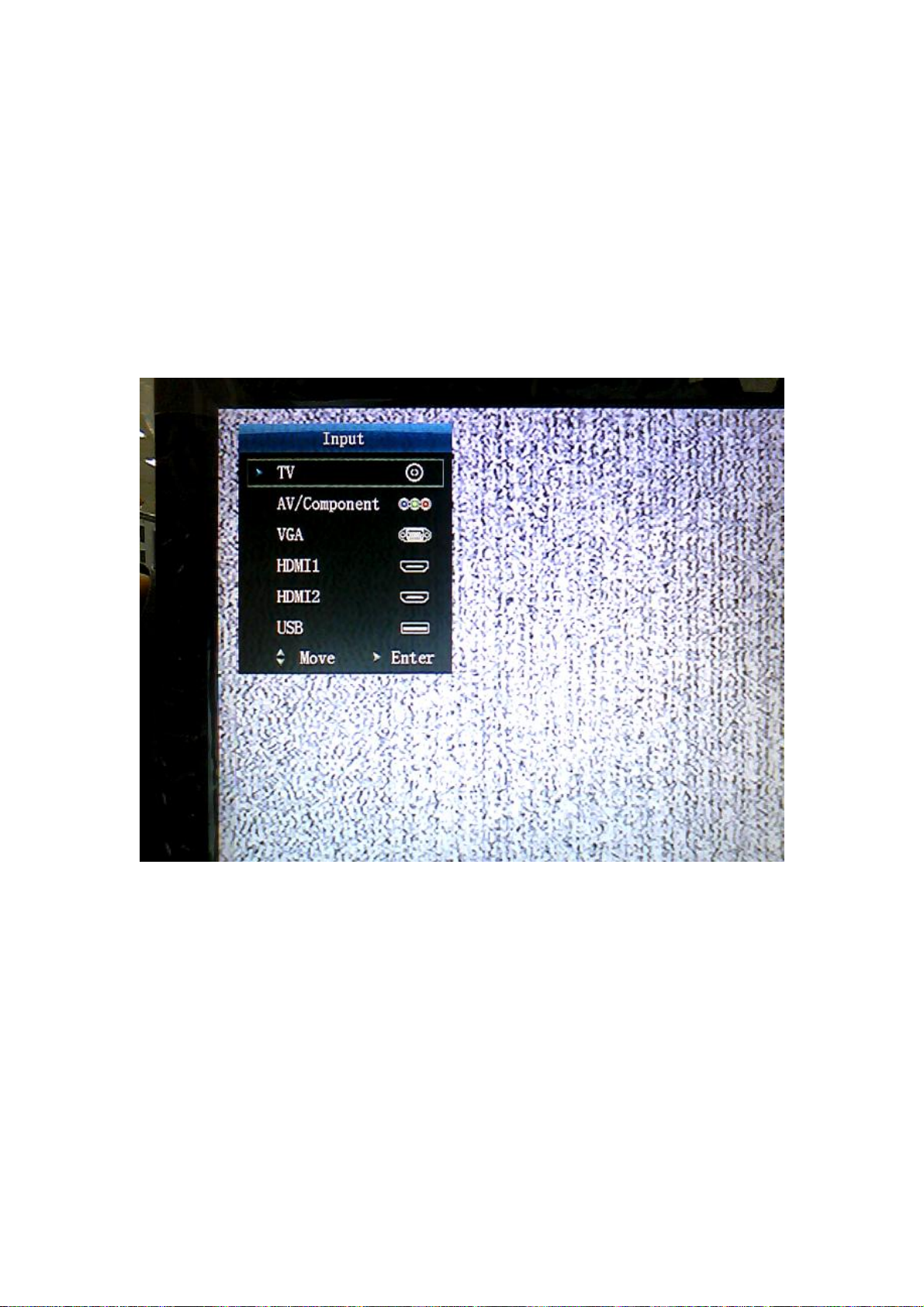
3. Press key “program source” until menu “program source” display, then
press keys “2”, “5”, “8”, “0” by turn to enter into factory menu, please refer to
the following Fig. 1;
Fig. 1 “Program source” menu
Page 13

Fig. 2 Factory menu
4. Press keys of remote control “▲”,”▼” to select item “ISP”, press key “enter”
to begin updating progress, a prompt “Updating, Pls, Waiting…” is
displaying, wait for a while until menu display (TV set is unable to accept
other operation now), please refer to the Fig. 3;
Page 14
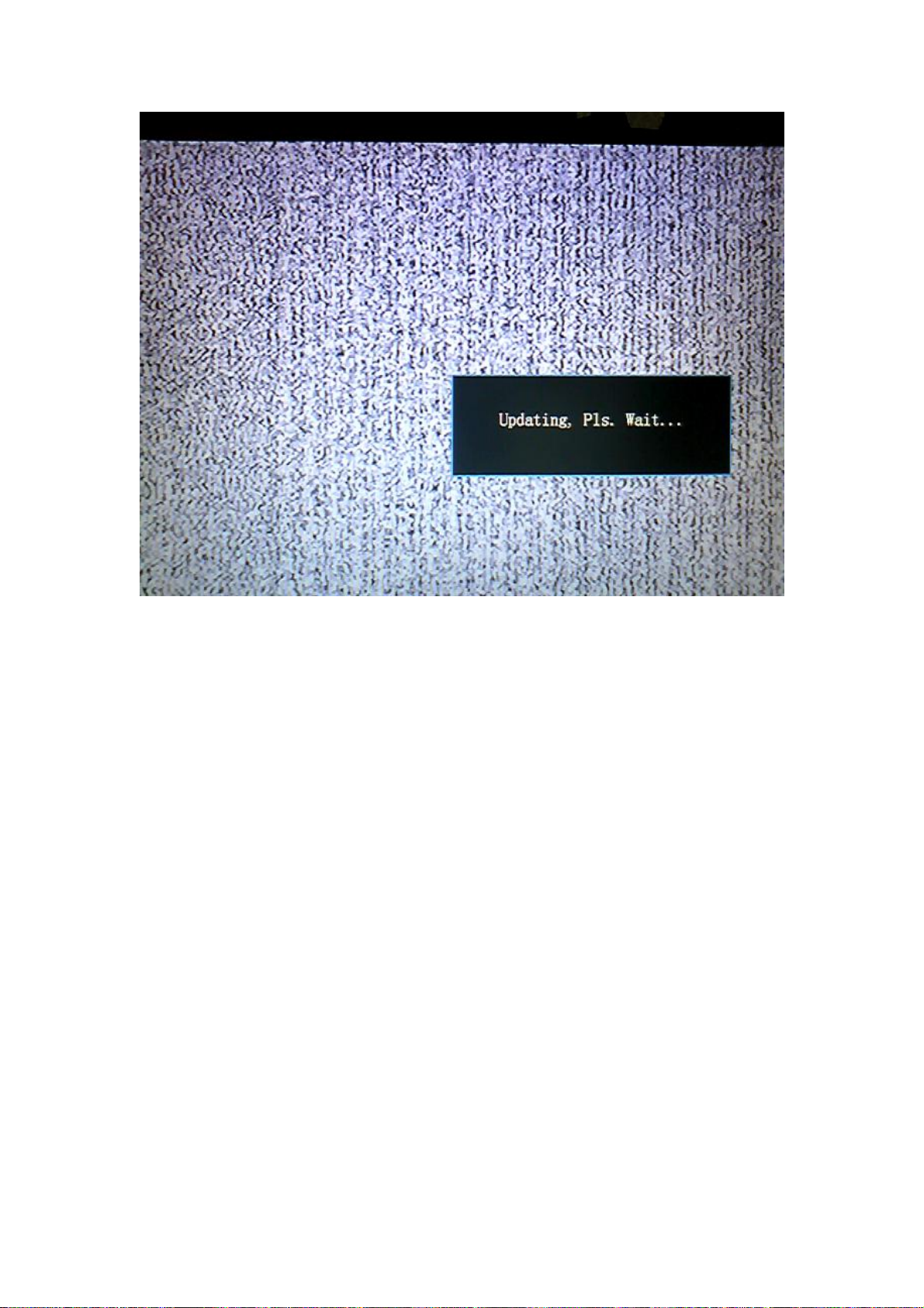
Fig. 3 Updating prompt
5. TV set will auto-reset after completing update, according to step1 and step
2, enter into factory menu again to confirm updating completion by
checking the time of update file.
Page 15

Working principle analysis of the unit
RF signal from antenna is sent into TUNER301 to be processed by
HF-amplified and frequency mixing, then IF signal is outputted to SWF Z301 to
be IF filtered to get ideal IF characteristics, then the signal is sent to main chip
N101(RTD2674S)-27#,28# to be amplified by inline IF amplifier and
synchronous demodulated to get CVBS.
Video and audio signal from AV and YPbPr are sent to main chip N101 directly;
video and audio signal from VGA and HDMI1, HDMI2 are also sent to main
chip N101 directly.
Main chip N101(RTD2674S) is a special large scale IC with full functions, such
as HDMI interface process, video decoding, video switch selection, A/D and
D/A transformation, interleaved/successive scans, mode transformation, OSD
and low-voltage difference output process, etc.; furthermore, it also has
functions of audio selection and process, MCU, etc.; external video signal is
processed by main chip N101(RTD2674S), then 4 pairs of difference signals
and one pair of clock signals are outputted to LCD to display; external audio
signal processed by main chip N101(RTD2674S) is sent to sound amplifier
N501(TAS5711) to be amplified and then to speakers.
MEMC signal flow
Video signal of current channel is coded by main chip N101(RTD2674S), then
LVDS signal is sent out to MEMC chip 6M20S to be processed by frame
inserting, frequency doubling, and then the LVDS signal is outputted to display
panel.
Page 16

Block diagram
Page 17

IC block diagram
RTD2674S
Main IC
Pin List
217
U2
1
VCM_BB
2
AVDD_BB0_3.3V
3
AIN_5L/LSADC6
4
AIO_2R
5
AIO_2L
6
AIO_1R
7
AIO_1L
8
AIN_4R
9
AIN_4L
10
AIN_3R
11
AIN_3L
12
AIN_2R
13
AIN_2L
14
AIN_1R
15
AIN_1L
16
AOUT_R
17
AOUT_L
18
HPOUT_R
19
HPOUT_L
20
SCART_FSW_0
21
SCART_FSW_1
22
DAC_VDD_3.3V
23
AVOUT_1
24
AVOUT_2
25
DAC_GND
26
ADC2X_GND_3.3V
27
IF_N
28
IF_P
29
ADC2X_VDD
30
PLL_GND
31
XI N
32
XO U T
33
PLL_VDD_3.3V
34
CORE_1.2V
35
USB_AVDD_3.3V
36
HSDM
37
HSDP
38
USB_AVDD_1.2V
39
I2C0_SCL
40
I2C0_SDA
41
IO_3.3V
42
GPIO_A0/RF_AGC
43
GPIO_A1/IF_AGC
44
CORE_1.2V
45
O_FP
46
O_FN
47
O_EP
48
O_EN
49
O_DP
50
O_DN
51
O_CP
52
O_CN
53
O_BP
54
O_BN
E-PAD
213
215
216
214
VIN_A2N
AGND_BB1
(CVBS)VIN_14P
AVDD_BB1_3. 3V
212
211
(CVBS/SV-C)VIN_13P
(CVBS/SV-Y)VIN_10P
209
VIN_A1N
208
(SV-C)VIN_12P
(SV-Y)VIN_9P
206
VIN_A0N
VD_GND
VD_VDD_1.2V
(SV-C/FSC_CVBS)VIN_11P
204
205
207
210
199
196
200
201
202
203
VIN_Y1N
ADC_VDD_1.2V
(FSC_R/Y)VIN _8P
(FSC_G/Pr)VIN_7P
(FSC_B/Pb)VIN_6P
194
195
198
(Pr)VIN_5P
193
197
VIN_2N
VIN_Y0N
(Y)VIN_4P
(Pb)VIN_3P
(VGA_R)VIN_2P
RTD2674
LQFP-216
E-PAD
188
190
192
191
VIN1_N
(VGA_B)VIN_1P
189
VIN_0N
(VGA_G)VIN_0P
186
187
VSYNC
VD_VDD_3.3V
ADC_VDD_3.3V
181
185
HSYNC
180
182
183
184
APLL_GND
TMDS_1.2V
TMDS_REXT
APLL_VDD_3. 3V
P0_RX0P/HDMI _2P_0
175
177
179
178
P0_RX1P/HDMI _1P_0
P0_RX1N/HDMI_1N_0
P0_RX0N/HDMI_2N_0
176
P0_RX2P/HDMI _0P_0
P0_RX2N/HDMI_0N_0
174
173
P0_RX3P/HDMI _CLKP_0
P0_RX3N/HDMI_CLKN_0
172
P1_RX0P/HDMI _2P_1
167
169
171
168
170
P1_RX2P/HDMI _0P_1
P1_RX1P/HDMI _1P_1
P1_RX1N/HDMI_1N_1
P1_RX0N/HDMI_2N_1
163
164
165
166
TMDS_1.2V
TMDS_3.3V
HDDC0_SCL
HDDC0_SDA
P1_RX2N/HDMI_0N_1
HDDC1_SCL
P1_RX3P/HDMI _CLKP_1
P1_RX3N/HDMI_CLKN_1
HDDC1_SDA
VGA_DDC_SCL
VGA_DDC_SDA
IO_3.3V
GPIO_C8
GPIO_C6
GPIO_C5
STBY_CORE_1.2V
SPI_D O
SPI_SCK
SPI_CS_N
RESET_IN
GPIO_C4
GPIO_C3
GPIO_C2
GPIO_C1
GPIO_C0
STBY_CORE_1.2V
LSADC4/GPIO
LSADC2/GPIO
LSADC1/GPIO
LSADC0/GPIO
LSADC_REF
IO_3.3V
CORE_1. 2V
DDR_IO_2.5V
DDR_VREF
DDR_IO_2.5V
DDR_IO_2.5V
ADDR12
ADDR11
CEC
SPI_DI
DQS1
DQ_8
DQ_9
DQ_10
DQ_11
DQ_12
DQ_13
DQ_14
DQ_15
DM1
CK#
CK
CKE
ADDR9
ADDR8
ADDR7
ADDR6
ADDR5
162
161
160
159
158
157
156
155
154
153
152
151
150
149
148
147
146
145
144
143
142
141
140
139
138
137
136
135
134
133
132
131
130
129
128
127
126
125
124
123
122
121
120
119
118
117
116
115
114
113
112
111
110
109
QFP216E
O_AP55O_AN56IO_3.3V57E_FP58E_FN59E_EP60E_EN61E_DP62E_DN63E_CP64E_CN65E_BP66E_BN67E_AP68E_AN69CORE_1. 2V70TCON/GPIO_B071TCON/GPIO_B272TCON/GPIO_B373TCON/GPIO_B474TCON/GPIO_B575TCON/GPIO_B676TCON/GPIO_B777TCON/GPIO_B878IO_3.3V79TCON/GPIO_B980TCON/GPIO_B1081TCON/GPIO_B1282CORE_1. 2V83DQS084DQ_785DQ_686DDR_IO_2.5V87DQ_588DQ_489DQ_390DQ_291DQ_192DQ_093DDR_IO_2.5V94DM095WE#96CAS#97RAS#98CORE_1. 2V99BA0
100
101
BA1
102
ADDR10
103
ADDR0
ADDR1
104
105
ADDR2
ADDR3
106
107
DDR_IO_2.5V
108
ADDR4
Page 18

Main IC
RTD2674S
Table 1-1. RTD2674S Pin Assignments – Pin detail description
(I/O Legend: A = Analog, I = Input, O = Output, P = Power, G = Ground)
Pin No Pin Name Type Description Note
1
2
3
4
5
6
7
8
9
10
11
12
13
14
15
16
17
18
19
20
21
22
23
24
25
26
27
28
29
30
31
32
33
34
35
36
37
38
39
40
VCM_BB AP Analog Audio Common Voltage Re ference
AVDD_BB0 AP Analog Baseband Power 3.3V
AIN_5L/LSADC6 AI Low Speed ADC input 6
AIO_2R AIO Analog Audio input/output 2 (Right Channe l)
AIO_2L AIO Analog Audio input/output 2 (Left Channel)
AIO_1R AIO Analog Audio input/output 1 (Right Channe l)
AIO_1L AIO Analog Audio input/output 1 (Left Channel)
AIN_4R AI Analog Audio input 4 (Right Channel)
AIN_4L AI Analog Audio input 4 (Left Channel)
AIN_3R AI Analog Audio input 3 (Right Channel)
AIN_3L AI Analog Audio input 3 (Left Channel)
AIN_2R AI Analog Audio input 2 (Right Channel)
AIN_2L AI Analog Audio input 2 (Left Channel)
AIN_1R AI Analog Audio input 1 (Right Channel)
AIN_1L AI Analog Audio input 1 (Left Channel)
AOUT_R AO Analog Baseband Audio Out (Right Channel)
AOUT_L AO Analog Baseband Audio Out (Left Channel)
HPOUT_R AO Head Phone DAC output (Right Channel)
HPOUT_L AO Head Phone DAC output (Left Channel)
Scart_FSW_0 AIO SCART RGB Fast Switch Input 0
Scart_FSW_1 AIO SCART RGB Fast Switch Input 1
DAC_VDD_0 AP Video DAC Power 3.3V
AVOUT_1 AP CVBS DAC output1
AVOUT_2 AP CVBS DAC output2
DAC_GND_0 AP Video DAC GND
ADC2X_GND_1 AP IFADC GND
IF_N AP IF demod Negative input
IF_P AP IF demod Postive input
ADC2X_VDD_0 AP IFADC power 3.3V
PLL_GND_1 AP XTAL PLL GND
XIN AP 27MHz Crystal Input
XOUT AP 27MHz Crystal Output
PLL_VDD_0 AP XTAL PLL power 3.3V
Core_1.2V DP Core Power 1.2V
AVDD_1 AP USB Power 3.3V
HSDM_1 AP USB HOST0 Data Negative
HSDP_1 AP USB HOST0 Data Postive
LV_USB_1 AP USB Power 1.2V
I2C0_SCL DIO Tuner I2C clock
I2C0_SDA DIO Tuner I2C data
Connect 1uF to GND
Analog 3.3V
Analog 3.3V
Analog 3.3V
Analog 3.3V
Digital 1.2V, Power Down@
Power saving
Analog 3.3V
Analog 1.2V
5V tolerance even when
power-off
5V tolerance even when
power-off
Page 19

Main IC
RTD2674S
41
42
43
44
45
46
47
48
49
50
51
52
53
54
55
56
57
58
59
60
61
62
63
64
65
66
67
68
69
70
71
72
73
74
75
76
77
78
79
VCC3_0 P PAD I/O Power 3.3V
GPIO_A0 DIO GPIO_A0
GPIO_A1 DIO GPIO_A1
Core_1.2V P Core Power 1.2V
B_FP AO LVDS_Port_B_F_Pair_P
B_FN AO LVDS_Port_B_F_Pair_N
B_EP AO LVDS_Port_B_E_Pair_P
B_EN AO LVDS_Port_B_E_Pair_N
B_DP AO LVDS_Port_B_D_Pair_P
B_DN AO LVDS_Port_B_D_Pair_N
B_CP AO LVDS_Port_B_C_Pair_P
B_CN AO LVDS_Port_B_C_Pair_N
B_BP AO LVDS_Port_B_B_Pair_P
B_BN AO LVDS_Port_B_B_Pair_N
B_AP AO LVDS_Port_B_A_Pair_P
B_AN AO LVDS_Port_B_A_Pair_N
LVDSV P LVDS Power 3.3V
A_FP AO LVDS_Port_A_F_Pair_P
A_FN AO LVDS_Port_A_F_Pair_N
A_EP AO LVDS_Port_A_E_Pair_P
A_EN AO LVDS_Port_A_E_Pair_N
A_DP AO LVDS_Port_A_D_Pair_P
A_DN AO LVDS_Port_A_D_Pair_N
A_CP AO LVDS_Port_A_C_Pair_P
A_CN AO LVDS_Port_A_C_Pair_N
A_BP AO LVDS_Port_A_B_Pair_P
A_BN AO LVDS_Port_A_B_Pair_N
A_AP AO LVDS_Port_A_A_Pair_P
A_AN AO LVDS_Port_A_A_Pair_N
Core_1.2V P Core Power 1.2V
GPIO_B0 DIO GPIO_B0
GPIO_B2 DIO GPIO_B2
GPIO_B3 DIO GPIO_B3
GPIO_B4 DIO GPIO_B4
GPIO_B5 DIO GPIO_B5
GPIO_B6 DIO GPIO_B6
GPIO_B7 DIO GPIO_B7
GPIO_B8 DIO GPIO_B8
VCC3_2 P PAD I/O Power 3.3V
Digital I/O 3.3V
5V tolerance even when
power-off
5V tolerance even when
power-off
Digital 1.2V, Power Down@
Power saving
Digital 1.2V, Power Down@
Power saving
5V tolerance even when
power-off
5V tolerance even when
power-off
5V tolerance even when
power-off
5V tolerance even when
power-off
5V tolerance even when
power-off
5V tolerance even when
power-off
5V tolerance even when
power-off
5V tolerance even when
power-off
Page 20

Main IC
80
81
82
83
84
85
86
87
88
89
90
91
92
93
94
95
96
97
98
99
100
101
102
103
104
105
106
107
108
109
110
111
112
113
114
115
116
117
118
119
120
121
122
RTD2674S
GPIO_B9 DIO GPIO_B9
GPIO_B10 DIO GPIO_B10
GPIO_B12 DIO GPIO_B12
Core_1.2V P Core Power 1.2V
DQS0 DO DDR_DQS0
DQ_7 DIO DDR_Data7
DQ_6 DIO DDR_Data6
SVCC25 P DDR I/O Power 2.5V
DQ_5 DIO DDR_Data5
DQ_4 DIO DDR_Data4
DQ_3 DIO DDR_Data3
DQ_2 DIO DDR_Data2
DQ_1 DIO DDR_Data1
DQ_0 DIO DDR_Data0
SVCC25 P DDR I/O Power 2.5V
DM0 DO DDR_Data_Mask0
WE# DO DDR Write Enable (Low Enable)
CAS# DO DDR CAS (Low Enable)
RAS# DO DDR RAS (Low Enable)
Core_1.2V P Core Power 1.2V
BA0 DO DDR Bank Address0
BA1 DO DDR Bank Address1
ADDR10 DO DDR Address10
ADDR0 DO DDR Address0
ADDR1 DO DDR Address1
ADDR2 DO DDR Address2
ADDR3 DO DDR Address3
SVCC25 P DDR I/O Power 2.5V
ADDR4 DO DDR Address4
ADDR5 DO DDR Address5
ADDR6 DO DDR Address6
ADDR7 DO DDR Address7
ADDR8 DO DDR Address8
ADDR9 DO DDR Address9
ADDR11 DO DDR Address11
ADDR12 DO DDR Address12
CKE DO DDR Clock Enable
SVCC25 P DDR I/O Power 2.5V
CK DO DDR Clock Differential(+)
CK# DO DDR Clock Differential(-)
DM1 DO DDR Data Mask1
SVCC25 P DDR I/O Power 2.5V
VREF AI DDR Reference Voltage Input
5V tolerance even when
power-off
5V tolerance even when
power-off
5V tolerance even when
power-off
Digital 1.2V, Power Down@
Power saving
Digital 1.2V, Power Down@
Power saving
1.25V Ref input
Page 21

Main IC
RTD2674S
123
124
125
126
127
128
129
130
131
132
133
134
135
136
137
138
139
140
141
142
143
144
145
146
147
148
149
150
151
152
153
154
155
156
157
158
159
DQ_15 DIO DDR_Data15
DQ_14 DIO DDR_Data14
DQ_13 DIO DDR_Data13
DQ_12 DIO DDR_Data12
DQ_11 DIO DDR_Data11
DQ_10 DIO DDR_Data10
SVCC25 P DDR I/O Power 2.5V
DQ_9 DIO DDR_Data9
DQ_8 DIO DDR_Data8
DQS1 DO DDR_DQS1
Core_1.2V P Core Power 1.2V
V33_IO P PAD I/O Power 3.3V
lsadc_ref AI LSADC reference
lsadc0 AI LSADC0
lsadc1 AI LSADC1
lsadc2 AI LSADC2
lsadc4 AI LSADC4
STBY_Core_1.2V P Standby ON Core Power 1.2V
GPIO_C0 DIO GPIO_C0
GPIO_C1 DIO GPIO_C1
GPIO_C2 DIO GPIO_C2
GPIO_C3 DIO GPIO_C3
GPIO_C4 DIO GPIO_C4
RSTI DI Chip Reset Input
SPI_CSn DO SPI Flash CS Output
SPI_SCLK DO SPI Flash Clock Output
SPI_SDO DO SPI Flash Data Output
SPI_SDI DI SPI Flash Data Input
STBY_Core_1.2V P Standby ON Core Power 1.2V
GPIO_C5 DIO GPIO_C5
GPIO_C6 DIO GPIO_C6
GPIO_C8 DIO GPIO_C8
VCC3_4 P PAD I/O Power 3.3V
VDDC_SDA DIO VGA DDC Data
VDDC_SCL DIO VGA DDC Clock
HDDC1_SDA DIO HDMI DDC Data 1
HDDC1_SCL DIO HDMI DDC Clock 1
Digital 1.2V, Power Down@
Power saving
Connect 10K to GND
Digital 1.2V, Always On@
Power saving
5V tolerance even when
power-off
5V tolerance even when
power-off
5V tolerance even when
power-off
5V tolerance even when
power-off
5V tolerance even when
power-off
Low Active
Digital 1.2V, Always On@
Power saving
5V tolerance even when
power-off
5V tolerance even when
power-off
5V tolerance even when
power-off
5V tolerance even when
power-off
5V tolerance even when
power-off
5V tolerance even when
power-off
5V tolerance even when
power-off
Page 22

Main IC
160
161
162
163
164
165
166
167
168
169
170
171
172
173
174
175
176
177
178
179
180
181
182
183
184
185
186
187
188
189
190
191
192
193
194
195
196
197
198
199
200
201
202
203
RTD2674S
HDDC0_SDA DIO HDMI DDC Data 0
HDDC0_SCL DIO HDMI DDC Clock 0
CEC DIO HDMI CEC function
RX_V12 AP HDMI GDI Power 1.2V
RX_V33 AP HDMI GDI Power 3.3V
HDMI_1_CLKN AI HDMI_RX_Port1_CLK_Pair_Negative
HDMI_1_CLKP AI HDMI_RX_Port1_CLK_Pair_Positive
HDMI_1_0N AI HDMI_RX_Port1_Pair0_Negative
HDMI_1_0P AI HDMI_RX_Port1_Pair0_Positive
HDMI_1_1N AI HDMI_RX_Port1_Pair1_Negative
HDMI_1_1P AI HDMI_RX_Port1_Pair1_Positive
HDMI_1_2N AI HDMI_RX_Port1_Pair2_Negative
HDMI_1_2P AI HDMI_RX_Port1_Pair2_Positive
HDMI_0_CLKN AI HDMI_RX_Port0_CLK_Pair_Negative
HDMI_0_CLKP AI HDMI_RX_Port0_CLK_Pair_Positive
HDMI_0_0N AI HDMI_RX_Port0_Pair0_Negative
HDMI_0_0P AI HDMI_RX_Port0_Pair0_Positive
HDMI_0_1N AI HDMI_RX_Port0_Pair1_Negative
HDMI_0_1P AI HDMI_RX_Port0_Pair1_Positive
HDMI_0_2N AI HDMI_RX_Port0_Pair2_Negative
HDMI_0_2P AI HDMI_RX_Port0_Pair2_Positive
TMDS_REXT AI TMDS External Resistor Input
RX_V12 AP HDMI GDI Power 1.2V
APLL_VDD AP APLL Power 3.3V
APLL_GND AP APLL GND
HSYNC AI Hsync input
VSYNC AI Vsync input
ADC_VDD33 AP ADC Power 3.3V
ADC_VDC_VDD33 AP ADC Power 3.3V
VIN_0P AI ADC Blue Input 1 Positive
VIN_BN AI ADC Blue Input 1 Negative
VIN_1P AI ADC Green Input 1 Positive
VIN_GN AI ADC Green Input 1 Negative
VIN_2P AI ADC Red Input 1 Positive
VIN_RN AI ADC Red Input 1 Negative
VIN_3P AI YPbPr Blue Input
VIN_Y0N AI Common GND for YPbPr
VIN_4P AI YPbPr Green Input
VIN_5P AI YPbPr Red Input
VIN_6P AI YPbPr Blue Input/Scart Blue
VIN_Y1N AI Common GND for YPbPr/Scart
VIN_7P AI YPbPr Green Input/Scart Green
VIN_8P AI YPbPr Red Input/Scart Red/Scart C
ADC_VDD12 AP ADC Power 1.2V
5V tolerance even when
power-off
5V tolerance even when
power-off
5V tolerance even when
power-off
Connect 6. 2K to GND
Page 23

Main IC
RTD2674S
204
205
206
207
208
209
210
211
212
213
214
215
216 AGND_BB1 AP Analog Baseband GND
Note
ADC_VDC_VDD12 AP ADC Power 1.2V
ADC_GND_OFF AP ADC GND
VIN_11P AI S-Video C/Scart C Input
VIN_A0N AI Common GND for Scart/SV
VIN_9P AI S-Video Y/Scart Y Input
VIN_12P AI S-Video C Input
VIN_A1N AI Common GND for SV
VIN_10P AI S-Video Y Input
VIN_13P AI CVBS Input
VIN_A2N AI Common GND for CVBS
VIN_14P AI CVBS Input
AVDD_BB1 AP Analog Baseband Power 3.3V
1. AP : Analog Power/Ground
2. AI : Analog Input
3. AO : Analog Output
4. AIO : Analog Input/Output
5. DP : Digital Power/Ground
6. I : Digital Input
7. O: Digital Output
8. IO : Digital Input/Output
Page 24

SSTIMER
OC_ADJ
PLL_FLTP
VR_ANA
PBTL
AVSS
PLL_FLTM
BST_A
GVDD_OUT
PVDD_A
OUT_A
RESET
PVDD_A
STEST
PDN
VR_DIG
OSC_RES
DVSSO
DVDD
MCLK
A_SEL
SCLK
SDIN
LRCLK
AVDD
SDA
SCL
DVSS
GND
VREG
BST_B
PVDD_B
PVDD_C
OUT_C
PVDD_D
BST_D
PGND_AB
OUT_B
PGND_CD
OUT_D
AGND
PGND_AB
PVDD_B
PGND_CD
PVDD_D
BST_C
PVDD_C
GVDD_OUT
P0075-08
PHP Package
(TopView)
TAS5711
1
2
3
4
5
6
7
8
9
10
11
12
13
14
15 161718 19 20
21 222324
25
26
27
28
29
30
31
32
484746
45 44
43 42 41 40 39 38 37
36
35
34
33
TAS5711
PIN ASSIGNMENT
PIN
NAME NO.
AGND 30 P Analog ground for power stage
A_SEL 14 DIO A value of 0 (15-kΩ pulldown) makes the I2C device address 0x34,
AVDD 13 P 3.3-V analog power supply
AVSS 9 P Analog 3.3-V supply ground
BST_A 4 P High-side bootstrap supply for half-bridge A
BST_B 43 P High-side bootstrap supply for half-bridge B
BST_C 42 P High-side bootstrap supply for half-bridge C
BST_D 33 P High-side bootstrap supply for half-bridge D
DVDD 27 P 3.3-V digital power supply
DVSSO 17 P Oscillator ground
(1) TYPE: A = analog; D = 3.3-V digital; P = power/ground/decoupling; I = input; O = output
(2) All pullups are weak pullups and all pulldowns are weak pulldowns. The pullups and pulldowns are included to assure proper input logic
levels if the pins are left unconnected (pullups → logic 1 input; pulldowns → logic 0 input).
(1)
TOLERANT
TYPE
5-V
TERMINATION
PIN FUNCTIONS
(2)
and a value of 1 (15-kΩ pullup) makes it 0x36. This pin can be
programmed after RESET to be an output by writing 1 to bit 0 of I2C
register 0x05. In that mode, the A_SEL pin is redefined as FAULT
(see ERROR REPORTING for details).
DESCRIPTION
Page 25

PIN FUNCTIONS (continued)
PIN
NAME NO.
TYPE
(1)
DVSS 28 P Digital ground
GND 29 P Analog ground for power stage
GVDD_OUT 5, 32 P Gate drive internal regulator output. This pin must not be used to
LRCLK 20 DI 5-V Pulldown Input serial audio data left/right clock (sample rate clock)
MCLK 15 DI 5-V Pulldown Master clock input
OC_ADJ 7 AO Analog overcurrent programming. Requires resistor to ground.
OSC_RES 16 AO Oscillator trim resistor. Connect an 18.2-kΩ 1% resistor to DVSSO.
OUT_A 1 O Output, half-bridge A
OUT_B 46 O Output, half-bridge B
OUT_C 39 O Output, half-bridge C
OUT_D 36 O Output, half-bridge D
PBTL 8 DI Low means BTL or SE mode; high means PBTL mode. Information
PDN 19 DI 5-V Pullup Power down, active-low. PDN prepares the device for loss of power
PGND_AB 47, 48 P Power ground for half-bridges A and B
PGND_CD 37, 38 P Power ground for half-bridges C and D
PLL_FLTM 10 AO PLL negative loop filter terminal
PLL_FLTP 11 AO PLL positive loop filter terminal
PVDD_A 2, 3 P Power supply input for half-bridge output A
PVDD_B 44, 45 P Power supply input for half-bridge output B
PVDD_C 40, 41 P Power supply input for half-bridge output C
PVDD_D 34, 35 P Power supply input for half-bridge output D
RESET 25 DI 5-V Pullup Reset, active-low. A system reset is generated by applying a logic
SCL 24 DI 5-V I2C serial control clock input
SCLK 21 DI 5-V Pulldown Serial audio data clock (shift clock). SCLK is the serial audio port
SDA 23 DIO 5-V I2C serial control data interface input/output
SDIN 22 DI 5-V Pulldown Serial audio data input. SDIN supports three discrete (stereo) data
SSTIMER 6 AI Controls ramp time of OUT_x to minimize pop. Leave this pin
STEST 26 DI Factory test pin. Connect directly to DVSS.
VR_ANA 12 P Internally regulated 1.8-V analog supply voltage. This pin must not
VR_DIG 18 P Internally regulated 1.8-V digital supply voltage. This pin must not be
VREG 31 P Digital regulator output. Not to be used for powering external
5-V
TOLERANT
TERMINATION
(2)
DESCRIPTION
drive external devices.
goes directly to power stage.
supplies by shutting down the Noise Shaper and initiating PWM stop
sequence.
low to this pin. RESET is an asynchronous control signal that
restores the DAP to its default conditions, and places the PWM in
the hard mute state (tristated).
input data bit clock.
formats.
floating for BD mode. Requires capacitor of 2.2 nF to GND in AD
mode. The capacitor determines the ramp time.
be used to power external devices.
used to power external devices.
circuitry.
Page 26

Wiring diagram
Page 27

Troubleshooting guide
1. No raster
Page 28

2. No picture, but sound is normal
Page 29

3. No sound, but picture is normal.
Page 30

E_AP
E_BP
E_CP
E_CLKP
E_EP
E_FP
O_AP
O_BP
O_CP
O_CLKP
O_EP
O_FP
BG1608B121
BG1608B121
BG1608B121
BG1608B121
BG1608B121
STPB3216-310PT
3.3V_STB
VCC_PANEL
K101
1.2V_STB
0
R153
1.5
1.5
R104
R108
STBY_CORE_1.2V
L101
C101
HDMI_1.2V
L102
C102
USB_1.2V
L103
C103
Y_1.2V
L104
C104
VD_Y_1.2V
L105
C105
L106
L107
BG1608B121
X101
PHB-2x20-2.0
2
2
4
4
6
6
8
8
10
10
12
12
14
14
16
16
18
18
20
20
22
22
24
24
26
26
28
28
30
30
32
32
34
34
36
36
38
38
40
40
100n
100n
100n
100n
100n
CORE_1.2V1.2V_STB
C106
100n
IO_3.3V
C107
100n
11
13
15
17
19
21
23
25
27
29
31
33
35
37
39
330n
53912B33K0
3.3V_STB
C109
100n
C110
100n
C113
C111
100n
100n
C112
C114
100n
100n
1
001:D6;003:D6;003:E5;004:D5;006:C4
1
3
001:D6;003:D6;003:E5;004:D5;006:C4
3
5
5
7
7
9
9
11
13
15
17
19
21
23
25
27
29
31
33
35
37
39
VADC_3.3V
L109
SGMI2012-2R2KT
1u
C701
C119
VDAC_3.3V
L110
BG1608B121
C120
Y_3.3V
L111
BG1608B121
C121
VD_Y_3.3V
L112
BG1608B121
C122
USB_3.3V
L113
BG1608B121
C123
C117
100n
100n
C118
E_AN
E_BN
E_CN
E_CLKN
E_EN
E_FN
O_AN
O_BN
O_CN
O_CLKN
O_EN
O_FN
C124
100n
100n
KEY_SCL
KEY_SDA
E_FN
E_EN
E_CLKN
E_CN
E_BN
E_AN
O_FN
O_EN
O_CLKN
O_CN
O_BN
O_AN
C115
C116
100n
100n
100n
100n
100n
100n
USB_1.2V
10u
C125
10V
3.3V_STB
100u
C100
VDAC_3.3V
VADC_3.3V
PLL_3.3V
USB_3.3V
R538
R539 ?
O_FP
O_FN
O_EP
O_EN
O_CLKP
O_CLKN
O_CP
O_CN
?
NC
R154
R155
R156
R157
R158
R159
R160
R161
R162
R163
R164
R165
BG1608B121
BG1608B121
BG1608B121
BG1608B121
BG1608B121
002:E5
002:E5
002:B6
002:B5
002:E2
002:E2
002:E4
002:E4
002:H2
002:H3
002:H3
002:H4
002:H4
003:G2
003:G2
001:E1
100
100
100
100
100
100
100
100
100
100
100
100
L114
L115
L116
L117
1u
C702
L118
AOUT_R
AOUT_L
YPBPR1_R
YPBPR1_L
HPOUT_L
HPOUT_R
HP_DETE
002:F5
22p
C126
22p
C127
USB_DN
USB_DP
TUN_SCL
TUN_SDA
RF_AGC_OUT
PLL_3.3V
C128
100n
APLL_3.3V
C129
100n
BB0_3.3V
C130
100n
BB1_3.3V
C131
100n
HDMI_3.3V
C132
100n
BB0_3.3V
VGA_R
VGA_L
AV1_R
AV1_L
VOUT
IF_N003:I2
IF_P003:I2
CORE_1.2V
IO_3.3V
E_FP
E_EP
E_CLKP
E_CP
E_BP
E_AP
O_FP
O_EP
O_CLKP
O_CP
O_BP
O_AP
C135
C136
C137
C138
C139
C140
C141
C142
C143
C144
C145
BG1608B121
BG1608B121
R105
G101
0
27MHz
C133
1u
C134
100n
10u
10u
10u
10u
10u
10u
10u
10u
10u
10u
10u
L119
L120
BB1_3.3V
217
1
VCM_BB
2
AVDD_BB0_3.3V
3
AIN_5L/LSADC6
4
AIO_2R
5
AIO_2L
6
AIO_1R
7
AIO_1L
8
AIN_4R
9
AIN_4L
10
AIN_3R
11
AIN_3L
12
AIN_2R
13
AIN_2L
14
AIN_1R
15
AIN_1L
16
AOUT_R
17
AOUT_L
18
HPOUT_L
19
HPOUT_R
20
SCART_FSW_0
21
SCART_FSW_1
22
DAC_VDD_3.3V
23
AVOUT_1
24
AVOUT_2
25
DAC_GND
26
ADC2X_GND_3.3V
27
IF_N
28
IF_P
29
ADC2X_VDD
30
PLL_GND
31
XIN
32
XOUT
33
PLL_VDD_3.3V
34
CORE_1.2V_34
35
USB_AVDD_3.3V
36
HSDM
37
HSDP
38
USB_AVDD_1.2V
39
I2C0_SCL
40
I2C0_SDA
41
IO_3.3V_41
42
GPIO_A0/RF_AGC
43
GPIO_A1/IF_AGC
44
CORE_1.2V_44
45
O_FP
46
O_FN
47
O_EP
48
O_EN
49
O_DP
50
O_DN
51
O_CP
52
O_CN
53
O_BP
54
O_BN
002:E4
AV1_V
C148
C147
C146
C149
C150
C151
C152
C153
C154
47n
47n
47n
47n
47n
47n
47n
47n
47n
214
215
216
212
213
E-PAD
VIN_A2N
AGND_BB1
(CVBS)VIN_14P
AVDD_BB1_3.3V
(CVBS/SV-C)VIN_13P
O_AN57IO_3.3V_57
E_FP59E_FN60E_EP61E_EN62E_DP63E_DN64E_CP65E_CN66E_BP67E_BN68E_AP69E_AN70CORE_1.2V_70
O_AP
56
58
55
O_BP
O_BN
O_AP
O_AN
E_FP
E_FN
206
207
208
209
210
211
VIN_A0N
VIN_A1N
(SV-Y)VIN_9P
(SV-C)VIN_12P
(CVBS/SV-Y)VIN_10P
(SV-C/FSC_CVBS)VIN_11P
E_EP
E_EN
E_CLKP
E_CLKN
E_CP
E_CN
C155
47n
202
203
204
205
VD_GND
VD_VDD_1.2V
ADC_VDD_1.2V
(FSC_R/Y)VIN_8P
E_BP
E_BN
E_AP
E_AN
002:E2
002:E1
002:E1
002:E1
VIN_Y0-
YPBPR1_Y+
YPBPR1_PR+
YPBPR1_PB+
C156
C157
C158
C159
C160
C161
C162
C163
47n
47n
47n
47n
47n
47n
47n
47n
194
195
196
197
198
199
200
201
VIN_Y0N
VIN_Y1N
(Y)VIN_4P
(Pb)VIN_3P
(Pr)VIN_5P
(FSV_B/Pb)VIN_6P
(FSC_G/Pr)VIN_7P
TCON/GPIO_B0
TCON/GPIO_B2
TCON/GPIO_B3
TCON/GPIO_B4
TCON/GPIO_B581TCON/GPIO_B10
TCON/GPIO_B6
71
72
73
74
75
76
77
PWM003:E3
?
SCLK
MCLK
SDIN
LRCLK
USB_FLAG
R537
006:C4
006:C4
006:C3
006:C4
002:G4
001:B5;003:D6;003:E5;004:D5;006:C4
003:F1
RF_AGC
APLL_3.3VY_3.3VVD_Y_3.3VY_1.2VVD_Y_1.2V
002:A2
002:A2
002:A2
002:C4
002:C4
002:C4
VGA_B+
VGA_B-
VGA_VS
C168
47n
185
186
187
188
189
YSYNC
VIN_0N
VD_VDD_3.3V
ADC_VDD_3.3V
(VGA_B)VIN_1P
002:C4
VGA_HS
6.2K
R112
181
182
183
184
HSYNC
APLL_GND
TMDS_1.2V_182
APLL_VDD_3.3V
HDMI2_RX1+
HDMI2_RX2-
HDMI2_RX2+
177
178
179
180
TMDS_REST
P0_RX1P/HDMI_1P_0
P0_RX0N/HDMI_2N_0
P0_RX0P/HDMI_2P_0
002:C4
002:C4
002:C4
002:C5
VGA_G+
VGA_G-
VGA_R-
VGA_R+
C164
C165
C166
C167
47n
47n
47n
47n
190
191
192
193
VIN1_N
VIN_2N
(VGA_G)VIN_0P
(VGA_R)VIN_2P
RTD2674S
N101
TCON/GPIO_B12
CORE_1.2V_83
DQS085DQ_786DQ_687DDR_IO_2.5V_87
IO_3.3V_79
TCON/GPIO_B9
TCON/GPIO_B7
TCON/GPIO_B8
82
83
79
80
78
R146
4.7K
R110
?
AMP_MUTE
AMP_STBY
R536
006:B4
006:C5
001:B5;003:D6;003:E5;004:D5;006:C4
KEY_SCL
KEY_SDA
DQ_589DQ_490DQ_391DQ_292DQ_193DQ_094DDR_IO_2.5V_94
84
88
33
R111
33
DQ_4
DQ_2
DQ_3
DQ_6
DQ_7
DQS0
DQ_5
33
R113
DQ_1
DQ_0
SGMI3216K100KT
10u
C169
002:A1
002:A2
002:A2
HDMI2_RX0+
HDMI2_RX1-
175
176
P0_RX2P/HDMI_0P_O
P0_RX1N/HDMI_1N_0
DM096WE#97CAS#98RAS#99CORE_1.2V_99
95
WE#
DM0
002:A1
002:A2
002:A1
002:A2
002:A3
002:A1
HDMI1_RX1-
HDMI1_RX1+
HDMI2_RX0-
HDMI2_CLK+
HDMI2_CLK-
HDMI1_RX2-
HDMI1_RX2+
169
170
171
172
173
174
PI_RX1N/HDMI_1N_1
PI_RX1P/HDMI_1P_1
PI_RX0N/HDMI_2N_1
PI_RX0P/HDMI_2P_1
P0_RX2N/HDMI_0N_0
P0_RX3N/HDMI_CLKN_0
P0_RX3P/HDMI_CLKP_0
BA0
BA1
ADDR10
100
101
102
33
R115
R114
CAS#
BA1
RAS#
BA0
ADDR10
L121
R117
510
C170
100n
002:A1
002:A1
002:A1
HDMI1_RX0+
HDMI1_RX0- 002:A1
HDMI1_CLK+
HDMI1_CLK-
HDMI_3.3V HDMI_1.2V
163
164
165
166
167
168
TMDS_3.3V
HDDC0_SCL
TMDS_1.2V_163
HDDC0_SDA
HDDC1_SCL
PI_RX2N/HDMI_0N_1
PI_RX2P/HDMI_0P_1
HDDC1_SDA
P1_RX3N/HDMI_CLKN_1
P1_RX3P/HDMI_CLKP_1
VGA_DDC_SCL
VGA_DDC_SDA
IO_3.3V_155
GPIO_C8
GPIO_C6
GPIO_C5
STBY_CORE_1.2V_151
STBY_CORE_1.2V_140
ADDR0
ADDR1
103
104
33
SPI_DI
SPI_DO
SPI_SCK
SPI_CS_N
RESET_IN
GPIO_C4
GPIO_C3
GPIO_C2
GPIO_C1
GPIO_C0
LSADC4/GPIO
LSADC2/GPIO
LSADC1/GPIO
LSADC0/GPIO
LSADC_REF
IO_3.3V_134
CORE_1.2V_133
DDR_IO_2.5V_129
DDR_VREF
DDR_IO_2.5V_121
DDR_IO_2.5V_117
ADDR12
ADDR11
ADDR2
ADDR3
DDR_IO_2.5V_107
ADDR4
105
106
107
108
33
R116
ADDR1
ADDR0
ADDR2
ADDR3
CEC
DQS1
DQ_8
DQ_9
DQ_10
DQ_11
DQ_12
DQ_13
DQ_14
DQ_15
DM1
CK#
CK
CKE
ADDR9
ADDR8
ADDR7
ADDR6
ADDR5
RF_AGC_OUT
162
161
160
159
158
157
156
155
154
153
152
STBY_CORE_1.2V
151
150
149
148
147
146
145
144
143
142
141
140
139
138
137
136
135
134
133
132
131
130
129
128
127
126
125
124
123
122
121
120
119
118
117
116
115
114
113
112
111
110
109
001:C5
3.3V_STB
75
R125
R118
10K
R119
33
R147
R149
R150
R148
DDR_IO_2.5V
C174
100n
R120
R121
33
0
0
33
R123
R124
10n
C172
33
33
33
33
L122
BG1608B121
10u
C171
C173
100n
001:F4
001:F4
HDMI_CEC 002:A1
HDMI2_SCL
HDMI2_SDA
HDMI1_SCL
HDMI1_SDA
VGA_SCL
VGA_SDA
R_LED
HDMI1_HPD
HDMI2_HPD
SPI_DI
SPI_DO
SPI_SCK
SPI_CS#
RESET# 001:G3
SPI_WP#
BL_ON
IRR
UART_TX 001:G2
UART_RX
KEY1
POWER_ON
PANEL_ON
IO_3.3V
DDR_2.5V
1K
R126
1K
R127
C175
100n
C178
100n
1
C179
2
100n
3
C176
100n
4
5
6
100n
7
C180
8
10u
C177
SPI_SCK
SPI_DO
002:C3
002:C3
002:C1
002:C1
002:C3
002:C3
001:H3;003:E5
002:C1
002:C3
001:H2
001:F3
001:F2
001:H2
001:H2
003:E3
003:E6
001:G2
003:E4
003:E4
003:D2
DQS1
DQ_8
DQ_9
DQ_10
DQ_11
DQ_12
DQ_13
DQ_14
DQ_15
VREF
DM1
CK#
CK
CKE
ADDR12
ADDR11
ADDR9
ADDR8
ADDR7
ADDR6
ADDR5
ADDR4
VREF
C1+
V+
C1-
C2+
C2-
V-
T2OUT
R2IN
100n
VREF
CK
CK#
CKE
RAS#
CAS#
WE#
DM0
DM1
DQS0
DQS1
ADDR0
ADDR1
ADDR2
ADDR3
ADDR4
ADDR5
ADDR6
ADDR7
ADDR8
ADDR9
ADDR10
ADDR11
ADDR12
BA0
BA1
N102
MAX3232CSE
Vcc
GND
T1OUT
R1IN
R1OUT
T1IN
T2IN
R2OUT
C181
4.7K
R128
4.7K
R129
R130
22
22
R132
HYB25DC256160CE-5.0
49
VREF
45
CK
46
CK
44
CKE
23
RAS
22
CAS
21
WE
24
CS
20
LDM
47
UDM
16
LDQS
51
UDQS
29
A0
30
A1
31
A2
32
A3
35
A4
36
A5
37
A6
38
A7
39
A8
40
A9
28
A10/AP
41
A11
42
A12
17
NC17
26
BA0
27
BA1
5V_STB
4.7K
R131
16
15
14
13
12
11
10
9
8
7
6
5
001:F4
100n
VCC
HOLD
CLK
DIO
N103
VDD18
VDD33
VDDQ3
VDDQ9
VDDQ15
VDDQ55
VDDQ61
VSS34
VSS48
VSS66
VSSQ6
VSSQ12
VSSQ52
VSSQ58
VSSQ64
DRAWN BY
APPROVED BY
C182
R133
100
R134
100
UART_RX
UART_TX 001:F4
N104
W25X32VSSIG-E
RESET#
DDR_2.5V
1
VDD1
18
33
3
9
15
55
61
2
DQ0
4
DQ1
5
DQ2
7
DQ3
8
DQ4
10
DQ5
11
DQ6
13
DQ7
54
DQ8
56
DQ9
57
DQ10
59
DQ11
60
DQ12
62
DQ13
63
DQ14
65
DQ15
34
48
66
6
12
52
58
64
R151
4.7K
001:F4
CS
DO
WP#
GND
3.3V_STB
10K
R135
10u
C183
DQ_0
DQ_1
DQ_2
DQ_3
DQ_4
DQ_5
DQ_6
DQ_7
DQ_8
DQ_9
DQ_10
DQ_11
DQ_12
DQ_13
DQ_14
DQ_15
R152
4.7K
100
100
R136
R137
NC
1
2
3
4
R138
R139
22
R140
001:F3;003:E5
D101
LL4148
2.5V DDR_2.5V
L123
BG1608B121
BG1608B121
002:H2
TX
RX 002:H1
22p
22p
C185
C184
3.3V_STB
0
0
Boot mode
0: ROM boot
1: Flash boot
PIN 154
10u
C703
C704
DDR_IO_2.5V2.5V
L124
C705
4.7K
R141
4.7K
R142
10u
10u
R_LED
4.7K
330
C186
C187
100n
R143
R144
100n
NC
EJTAG EN
0: Enable
1: Disable
PIN 147
SPI_CS#
SPI_DI
SPI_WP#
4.7K
R145
C188
100n
C189
100n
C190
C191
100n
001:F4
001:F3
001:F4
100n
C192
C193
100n
100n
C195
TITLE: DWG NO.
2674S@DDR
RTD2674S
LVDS@Flash
REV.
Sheet to
XOCECO
XIAMEN OVERSEAS CHINESE
ELECTRONIC CO., LTD.
C194
100n
100n
1
C196
100n
C197
100n
A1.0
C198
100n
C199
100n
3
Page 31

1
2
3
4
5
6
8
9
10
11
HDMI1HDMI2
12
13
14
15
16
17 7
18
19
X201
HDMI-FIX
3.3V_STB
R201
27K
1
2
3
4
5
6
8
9
10
11
12
13
14
15
16
17 7
18
19
X202
HDMI-FIX
5
10
15
89
VGAVGA AUDIO
2
PESD5V0L4UG
N201
JY-3541L-01-030
1u
C201
234
12 13 14
1
67
11
HC1041-15F-3
X203
1
3
4
5
X204
2
L
R
G
1
3
4
5
HDMI1_5V
HDMI2_5V
VGA_5V
1
N203
PESD5V0L4UG
HDMI1_RX2+
HDMI1_RX2HDMI1_RX1+
HDMI1_RX1HDMI1_RX0+
HDMI1_RX0HDMI1_CLK+
HDMI1_CLKHDMI_CEC
100n
C202
HDMI2_RX2+
HDMI2_RX2HDMI2_RX1+
HDMI2_RX1HDMI2_RX0+
HDMI2_RX0HDMI2_CLK+
HDMI2_CLK-
100n
C203
4
3
5
2
001:E2
001:E2
001:E2
001:E2
001:E2
001:E2
001:E2
001:E2
001:F3
N204
001:E2
001:E2
001:E2
001:E2
001:E2
001:E2
001:E2
001:E2
N205
STBL3216-190PT
STBL3216-190PT
5
PESD5V0L4UG
5
PESD5V0L4UG
4.7K
R202
L201
L202
2K
R203
5
4
3
1
PESD5V0L4UG
N206
C204
470p
C205
470p
HDMI1_5V
HDMI2_5V
4.7K
R209
4
4.7K
R210
4
R211
R212
75
R204
75
R205
75
R206
R207
6.8K
R208
6.8K
2
2
4.7K
2K
2
3
3
4.7K
R219
4.7K
R220
R213
100
R214
100
R215
100
R216
100
R217
1K
1
R218
1K
1
22p
C206
R221
R222
5V
5V
10K
10K
100n
C208
10
47K
R225
BC847AW
R224
4.7K
V201
100n
C209
10
47K
R223
BC847AW
R226
4.7K
V202
10p
C207
R227
100
R228
C210
4.7p
100
R229
100
R230
C211
4.7p
100
R231
100
R232
C212
4.7p
100
close to main chip
001:C3
VGA_L
001:C3
VGA_R
CH5
6
CH6
7
VP
8
CH7
9
CH8
CH5
6
CH6
7
VP
8
CH7
9
CH8
CH4
CH3
CH2
CH1
CM1213-08MS
N207
HDMI1_SCL
HDMI1_SDA
HDMI1_HPD
CH4
CH3
CH2
CH1
CM1213-08MS
N208
HDMI2_SCL
HDMI2_SDA
HDMI2_HPD
VGA_SCL
VGA_SDA
VGA_VS
VGA_HS
VGA_B-
VGA_B+
VGA_G-
VGA_G+
VGA_R-
VGA_R+
VN
001:F3
001:F3
001:F3
VN
001:F3
001:F3
001:F3
001:F3
001:F3
001:D2
001:D2
001:D2
001:D2
001:D2
001:D2
001:D2
001:D2
5
4
3
2
NC
1
G B R
75
R237
75
R238
YPBPRYPBPR AUDIO
75
RCA-389A-01
X205
5
4
3
2
NC
1
RCA-389A-02
RCA-389A-02
Y
X207
W
AV1AVOUT
R
Y
X210
W
W
R
RCA-289A-01
X206
C213
1u
2
PESD5V0L4UG
1
3
4
5
N210
R
1
3
2
4
1u
C214
5
PESD5V0L4UG
N209
R239
close to main chip
C217
C216
1
3
4
5
75
R243
C220
470p
C221
470p
5
4
3
1
PESD5V0L4UG
R257
100
R258
C228
4.7p
100
R259
100
R260
C229
4.7p
100
R261
100
R262
C230
4.7p
100
R234
6.8K
10K
470p
470p
PESD5V0L4UG
R248
R233
6.8K
10K
R247
C215
1u
2
N211
close to main chip
R244
6.8K
R245
6.8K
N213
R246
SGMI2012M1R0KT
51
C225
270p
NC
10K
R251
10K
R252
R271
75
R253
C223
470p
R254
C224
470p
2
L221
100
100
1u
R255
R256
C226
C227
270p
1K
1K
YPBPR1_Y+
VIN_Y0-
YPBPR1_PB+
YPBPR1_PR+
YPBPR1_L
YPBPR1_R
AV1_L
AV1_R 001:C3
C234
47u
10V
AOUT_L 001:C3
C235
47u
10V
AOUT_R 001:C3
10K
R269
10K
R270
001:C3
001:C3
AV1_V
001:C3
C236
4.7u
R726
0
10V
470u
C708
BC847AW
V203
BC847AW
V204
001:D2
001:D2
100n
C237
001:D2
001:D2
001:D2
R272
4.7K
R273
4.7K
V205
BC857AW
R274
220
150
R727
5V
330
R275
220
R276
R277
V206
BC847AW
R278
HP_MUTE
75K
10V
100u
C238
68K
002:H3;006:B4
001:D6
USB_FLAG
VOUT 001:C4
X208
JY-3541L-01-030
UP DATA HP OUT
ST-113
X211
1u
C240
GG
1
2
USB
34
UBA-100/W
DRAWN BY
G
R
L
1
C239
1u
2
34
PESD5V0L5UY
L
G2
R
G5
1
3
2
4
5
PESD5V0L4UG
N214
30K
R279
47K
R280
10V
100u
C241
X209
N216
IP4223CZ6
6
5
N215
FU201
SMD1206P075TF
750mA
5
6
1
2
34
RX 001:H1
001:H1
TX
C245
C246
10K
R286
10K
R287
5V_USB
100n
100n
R235
2K
BC847AW
V207
BC847AW
V208
R290
0
0
R292
4.7p
C244
1K
R293
1K
R294
4.7p
C249
10V
100u
C254
10V
100u
C255
3.3V_STB
R297
4.7K
R298
4.7K
USB_DN
USB_DP
10K
R299
001:C4
001:C4
HPOUT_L
HPOUT_R
HP_MUTE
TITLE: DWG NO.
Interface RTD2674S
REV.
Sheet to
001:C4
001:C4
001:C4
HP_DETE
002:F5;006:B4
A1.0
2
3
PESD5V0L4UG
N202
APPROVED BY
XOCECO
XIAMEN OVERSEAS CHINESE
ELECTRONIC CO., LTD.
Page 32

5V_STB
12V
R721
0
D301
B240-13-F
D302
B240-13-F
12V
25V
10u
C706
3.3V-6M20S
5V
3.3V_STB
470u
C301
0
NC
R720
25V
470u
R330
0
R317
3.3
2W
R388
1.2
1W
R389
1.2
1W
5302FA12H0
C307
10n
100n
C302
Vout=0.923*[1+(R309+R310)/R313]
C314
10n
100n
C311
C306
Vout=0.923*[1+(R315+R316)/R322]
M
10V
220u
C313
M
M
10V
220u
5V
10V
220u
MP1484
1
BS
2
IN
3
SW
4
GND_4
L301
SLF7032T-100M1R4-PF
1
53998010M1
1
BS
2
IN
3
SW
4
GND_4
L302
SLF7032T-100M1R4-PF
1
53998010M1 2.1A
C315
100n
C303
100n
C308
C304
100n
C309
N301
8
SS
7
EN
6
COMP
5
FB
2
2.1A
N305
MP1484
SS
EN
COMP
FB
2
001:F4;003:E4
N306
AP1117-ADJ
IN OUT
53112030F0
Vout=1.25*(1+R312/R311)
N302
AZ1084S-ADJ
OUT
IN
ADJ
53112030F0
Vout=1.25*(1+R306/R305)
N303
AZ1084S-ADJ
OUT
IN
ADJ
Vout=1.25*(1+R308/R307)
820
R311
402
R312
5V
L314
BG1608B121
1u
100n
C324
C320
R309
4.3K
330
R310
10V
470u
8
7
6
5
R315
2.2K
430
R316
16V
470u
C321
10V
470u
390
R305
33
R306
4.7K
10n
1K
10K
R313
C325
C329
100n
1u
100n
C330
C326
8.2n
1K
10K
R322
SLF7032T-100M1R4-PF
1
100n
C333
C331
POWER_ON
1.8V-6M20S
OUT 1.80v
C327
100n
10V
470u
C318
100n
R318
C328
R319
R323
0
R324
4.7K
C332
R325
L312
2
53998010M1
2.1A
C322
5V_USB
OUT 5.2v
10V
R724
10K
1K
R320
NC
220u
10K
R723
C378
V322
BC847AW
NC
R722
S
R725
10K
1.2V_STB
OUT 1.35v
001:F4
OUT 3.35v
0
D
G
AO3401A
V323
100n
C707
PANEL_ON
3.3V_STB
3.3V-6M20S
L321
STBH2012-501PT
12V VCC_PANEL
1
2
3
4
R327
4.7K
1u
X301
R328
R329
C334
47K
4.7K
V303
BC847AW
1u
C336
N307
AO4803A
S2
G2
S1
G1
C343
470n
D2_8
D2_7
D1_6
D1_5
24V
8
7
6
5
1
2
3
35V
C337
820u
C339
100n
R337
100K
4
5
5V
GND-H
1K
R345
V307
X302
TJC3S-13AW
1
1u
C340
100K
R339
BC847AW
10K
R350
5V
2
3
4
5
6
7
8
9
10
11
12
13
X303
1
STBH2012-102PT
2
3
STBH2012-102PT
4
12V
32V
R331
100K
L313
STBL3216-190PT
R334
100K
L315
L316
5V
5V_STB
R340
10K
1u
C342
V306
BC847AW
R338
?
L318
BG2012D151T
L317
BG2012D151T
V309
BC847AW
2K
R346
1K
5V_STB
R343
R347
1K
5
X304
1
2
6
2
PESD5V0L4UG
N309
1
3
4
5
22p
C382
5V_STB
22p
C383
R395
100
R396
100
V318
BC847AW
R709
0
NC
3.3V_STB
4.7K
1K
R349
R351
4.7K
5V_STB
V310
BC847AW
3.3V_STB
1K
R392
1K
R705
R353
R707
1K
4.7K
1K
R393
100n
R354
C345
BL_ON
3.3V_STB
R355
10K
0:STAND BY
1:ON
4.7K
R394
5V_STB
BC847AW
001:F4
PWM
10K
R706
V319
1
NC1
2
NC2
3
RF_AGC
4
BT_4
5
AS
22p
C381
R_LED
BT_10
IF_OUT
6
SCL
7
SDA
8
Vcc
9
ADC
10
11
NC
12
001:F4
KEY1
001:F3;001:H3
001:F4
TUNER301
F25WT-16NXR-E
001:D6
R356
4.7K
POWER_ON
22p
C380
KEY_SCL
001:B5;001:D6;003:D6;004:D5;006:C4
KEY_SDA
001:B5;001:D6;003:D6;004:D5;006:C4
R708
1K
L304
SGMI3216K100KT
BC857AW
10u
16V
C355
R369
R364
100
R365
100
10n
100n
C356
10u
C359
C357
100n
1K
10u
C379
R371
4.7K
470u
R372
L306
22uH
C360
RF_AGC
100p
5V
32V
V314
5V
4.7K
close to main chip
10V
C358
L307
SGMI3216K100KT
10u
C389
C363
100p
R710
0
001:E1
C364
NC
C386
10n
C353
10n
10K
R711
R712
2.7K
100p
100p
C392
C391
L305
SGMI2012-2R2KT
330n
53912B33K0
12V_IF
820
R713
L325
C387
V320
2SC2216
1u
SGMI2012-2R2KT
100
R714
TUN_SCL 001:C5
TUN_SDA 001:C5
5410400027
Z301
D8673H
12345
L308
SGMI3216M2R2KT
330
R717
L320
10K
R715
SGMI2012-2R2KT
2.7K
R716
V321
2SC2216
220
R718
10n
C388
1K
R377
10p
C367
10p
C368
12V_IF
16V
NC
1K
R379
C369
1u
C370
1u
12V
L328
STBH3216-301PT
100u
C390
IF_N
IF_P
001:C4
001:C4
3
4
3.3V_STB
100
R307
100
R308
16V
470u
C319
C323
100n
R314
0
2.5V
OUT 2.5v
5
6
7
TJC10S-07AW
100
R321
100
R326
KEY_SDA
001:B5;001:D6;003:E5;004:D5;006:C4
KEY_SCL
001:B5;001:D6;003:E5;004:D5;006:C4
100n
C384
NC
R700
4.7K
R701
1K
R704
4.7K
4.7K
R702
BC847AW
V317
1K
R703
100p
C385
IRR
001:F4
DRAWN BY
APPROVED BY
TITLE: DWG NO.
Power@Tuner
RTD2674S
REV.
Sheet to
XOCECO
XIAMEN OVERSEAS CHINESE
ELECTRONIC CO., LTD.
3
A1.0
3
Page 33

004:F4
004:E4
004:E4
004:D3
004:D3
004:E4
004:D3
004:D3
004:D3
004:D3
004:D3
004:D3
004:D3
004:D3
004:D4
004:D4
004:D4
004:D4
004:D4
004:D4
004:D3
004:D3
004:E4
004:E4
004:E4
004:E4
004:F4
004:F4
004:F4
004:F4
004:F4
004:F4
004:F4
004:F4
004:F4
004:F4
004:F4
004:D3
004:D3
004:D3
004:D3
004:D4
004:D4
004:A5
004:F4
004:A5
004:A5
004:A5
004:A5
004:A5
004:A5
004:A5
004:A5
004:A5
004:A5
004:A4
004:A5
004:A4
004:A6
004:A6
004:A5
B_WEZ
B_RASZ
B_CASZ
B_DQM0
B_DQM1
B_ODT
1.8V_6M20S
10K
R406
10K
R407
B_MDATA14
B_MDATA9
B_MDATA12
B_MDATA11
B_MDATA6
B_MDATA1
B_MDATA3
B_MDATA4
B_MDATA5
B_MDATA2
B_MDATA0
B_MDATA7
B_MDATA13
B_MDATA10
B_MDATA8
B_MDATA15
B_MADR0
B_MADR2
B_MADR4
B_MADR6
B_MADR8
B_MADR11
B_BA0
B_MADR1
B_MADR10
B_MADR5
B_MADR9
B_MADR12
B_MADR7
B_MADR3
B_CKE
B_DQS0M
B_DQS0P
B_DQS1M
B_DQS1P
B_MCLKZ
B_MCLK
004:A5
004:A5
004:A6
004:A5
C401
M1-BA0
B_BA1
B-MADR12
B-MADR11
B-MADR10
B-MADR9
B-MADR8
B-MADR7
B-MADR6
B-MADR5
B-MADR4
B-MADR3
B-MADR2
B-MADR1
B-MADR0
M1_CLK-
M1_CLK+
M1-CKE
R402 56
R471
R470
R404
R405
R472 56
B-DQS0P
B-DQS0M
B-DQS1P
B-DQS1M
100n
005:E4
005:E4
A2M
174
175
LVA2M
LVA2P
005:E5
005:E5
005:E5
A3P
ACKM
ACKP
33
R461
172
173
LVA3P
LVACKM
LVACKP
GPIO[22]
99
AVDD2_LVDS
005:E5
005:E5
005:E5
A4P
A4M
A3M
168
169
170
171
LVA4M
LVA4P
LVA3M
GPIO[23]
GPIO[24]
GPIO[25]
100
101
102
103
004:F6
005:E5
005:E5
005:E5
005:E5
B0M
B0P
B1M
B1P
33
R460
163
164
165
166
167
LVB1M
LVB1P
LVB0M
LVB0P
GND_167
AVDD_LVDS_168
AVDD_LVDS_160
VDDC_159
GPIO_158
GPIO_157
AVDD_LVDS_148
GPIO_130
GPIO_129
AVDD_LVDS_123
VDDP_118
VDDC_117
GPIO[26]
GPIO[27]
GND_105
RESET
VDDP_107
VDDC_108
104
105
106
107
108
R450
0
GPIO9_6M20S
REXT
GND_161
LVB2P
LVB2M
LVBCKP
LVBCKM
LVB3P
LVB3M
LVB4P
LVB4M
GND_147
LVC0P
LVC0M
LVC1P
LVC1M
LVC2P
LVC2M
LVCCKP
LVCCKM
LVC3P
LVC3M
LVC4P
LVC4M
LVD0P
LVD0M
LVD1P
LVD1M
GND_128
LVD2P
LVD2M
LVDCKP
LVDCKM
LVD3P
LVD3M
LVD4P
LVD4M
GPIO[1]
PWM0
PWM1
CSZ
SDO
SDI
SCK
GND_109
Ursa_RESET
004:E6
VDDC_6M20S
R459
162
161
160
159
158
157
156
155
154
153
152
151
150
149
148
147
146
145
144
143
142
141
140
139
138
137
136
135
134
133
132
131
130
129
128
127
126
125
124
123
122
121
120
119
118
117
116
115
114
113
112
111
110
109
VDDP2
820
AVDD2_MEMPLL
33
R458
33
R457
R456
33
R455
33
R454
33
R453
33
R452
33
R451
33
AVDD2_LVDS
AVDD2_MPLL
AVDD2_LPLL
TITLE: DWG NO.
6M20 RTD2674S
VDDP2
VDDP2
AVDD2_LVDS
AVDD2_MEMPLL
B2P
B2M
BCKP
BCKM
B3P
B3M
B4P
B4M
C0P
C0M
C1P
C1M
C2P
C2M
CCKP
CCKM
C3P
C3M
C4P
C4M
D0P
D0M
D1P
D1M
D2P
D2M
DCKP
DCKM
D3P
D3M
D4P
D4M
005:G2
AVDD2
AVDD2_MPLL
AVDD2_LPLL
005:E5
005:E5
005:E6
005:E6
005:E6
005:E6
005:D6
005:D6
005:B4
005:B4
005:C4
005:B4
005:C4
005:B4
005:C4
005:B4
005:C4
005:B5
005:C5
005:B5
005:C5
005:B5
005:C5
005:B5
005:C5
005:B5
005:C5
005:B5
005:C5
005:B5
005:B5
005:B5
004:B4
004:B4
004:B5
004:H6
004:H6
004:H6
004:H6
A1.0
4
AVDD2
GPIO1_6M20S
PWM0_6M20S
PWM1_6M20S
SPI_CZ-6M20S
SPI_DO-6M20S
SPI_DI-6M20S
SPI_CK-6M20S
REV.
Sheet to
005:F3
005:F3
005:F3
005:G2
005:F1
6
N401
K4T51163QG-HCF7
L2
BA0
L3
R2
P7
M2
P3
P8
P2
N7
N3
N8
N2
M7
M3
M8
K8
J8
K2
L8
K3
K7
L7
F3
B3
K9
F7
E8
B7
A8
J2
A2
E2
L1
R3
R7
R8
BA1
A12
A11
A10
A9
A8
A7
A6
A5
A4
A3
A2
A1
A0
CK
CK
CKE
CS
WE
RAS
CAS
LDM
UDM
ODT
LDQS
LDQS
UDQS
UDQS
VREF
NC#A2
NC#E2
NC
NC#R3
NC#R7
NC#R8
B-MDATA14
B-MDATA9
B-MDATA12
B-MDATA11
B-MDATA6
B-MDATA1
B-MDATA3
B-MDATA4
B-MDATA5
B-MDATA2
B-MDATA0
B-MDATA7
B-MDATA13
B-MDATA10
B-MDATA8
B-MDATA15
B-MADR0
B-MADR2
B-MADR4
B-MADR6
B-MADR8
B-MADR11
M1-BA0
B-MADR1
B-MADR10
B-MADR5
B-MADR9
B-MADR12
B-MADR7
B-MADR3
M1-CKE
B-DQS0M
B-DQS0P
B-DQS1M
B-DQS1P
M1_CLKM1_CLK+
004:B1
004:B1
004:B1
004:B1
004:B1
004:B1
004:B1
004:B1
004:B1
004:B1
004:B1
004:B1
004:B1
004:B1
004:B1
004:B1
004:A1
004:A1
004:A1
004:A1
004:A1
004:A1
004:A1
004:A1
004:A1
004:A1
004:A1
004:A1
004:A1
004:A1
004:A2
004:A2
004:A2
004:A3
004:A3
004:A2
004:A2
56
R401
56
R476
56
56
56
56
R408
56
R409
56
R410
56
R411
56
56
R403
56
R412
56
R413
56
R414
56
R415
56
R416
56
R417
56
R418
56
R419
56
R420
56
R421
56
R422
56
R423
56
R424
56
R425
R426
56
R427
56
R428
56
DQ15
DQ14
DQ13
DQ12
DQ11
DQ10
VDDQ1
VDDQ2
VDDQ3
VDDQ4
VDDQ5
VDDQ6
VDDQ7
VDDQ8
VDDQ9
VDDQ10
VDD1
VDD2
VDD3
VDD4
VDD5
VDDL
VSSDL
VSSQ1
VSSQ2
VSSQ3
VSSQ4
VSSQ5
VSSQ6
VSSQ7
VSSQ8
VSSQ9
VSSQ10
VSS1
VSS2
VSS3
VSS4
VSS5
004:H4
004:H4
004:H4
004:D2
DQ9
DQ8
DQ7
DQ6
DQ5
DQ4
DQ3
DQ2
DQ1
DQ0
B9
B1
D9
D1
D3
D7
C2
C8
F9
F1
H9
H1
H3
H7
G2
G8
A9
C1
C3
C7
C9
E9
G1
G3
G7
G9
A1
E1
J9
M9
R1
J1
J7
A7
B2
B8
D2
D8
E7
F2
F8
H2
H8
A3
E3
J3
N1
P9
B-MDATA15
B-MDATA14
B-MDATA13
B-MDATA12
B-MDATA11
B-MDATA10
B-MDATA9
B-MDATA8
B-MDATA7
B-MDATA6
B-MDATA5
B-MDATA4
B-MDATA3
B-MDATA2
B-MDATA1
B-MDATA0
100n
100n
C408
C404
100n
100n
C405
004:A4
004:A3
004:A4
004:A3
004:A3
004:A3
004:A4
004:A4
004:A4
004:A4
004:A4
004:A4
004:A4
C409
004:A4
004:A4
004:A4
10u
C411
100n
C406
1.8V_6M20S
STBH2012-501PT
10V
100u
C419
100n
100n
C402
C407
L401
100n
1.8V-6M20S
C403
CHIP_CONF:{GPIO8,PWM1,PWM0}
CHIP_CONF=3~d5:boot from internal SRAM
CHIP_CONF=3~d6:boot from EEPROM
CHIP_CONF=3~d7:boot from SPI
GPIO1_6M20S
PWM0_6M20S
PWM1_6M20S
GPIO8_6M20S
C414
2.2u
GPIO1 is always LOW.
3.3V-6M20S
R467
NC
10K
R468
10K
R433
10K
10K
NC
R434
R435
10K
10K
NC
R436
R437
10K
10K
NC
R438
004:F1
XTALO
3.3V-6M20S
R441
100K
R442
4.7K
BAV99
D401
BC857AW
V401
22K
R444
R443
10u
C415
1K
1n
C416
X401
1
2
3
4
R439
0
Ursa_RESET 004:G5
3.3V-6M20S
4.7K
R429
20p
C412
AVDD2_MEMPLL
4.7K
R430
R440
1M
Z401
12MHz
R431
100
R432
100
R465
R466
20p
C413
001:A6;001:B5;001:B6
001:A6;001:B6;001:B5
001:A6;001:B5;001:B6
001:A6;001:B6;001:B5
001:A6;001:B6;001:B5
001:A6;001:B5;001:B6
O_CLKN
O_FN
O_FP
O_EN
O_EP
O_CLKP
VDDC_6M20S
VDDP2
AVDD_DDR_6M20S
1
R448
10K
2
3
4
5
6
7
8
9
10
11
12
13
14
15
16
17
18
19
20
21
22
23
24
25
26
27
28
29
30
31
32
33
34
35
36
37
38
39
40
41
42
43
44
45
46
47
48
49
50
51
52
53
54
I2CS_SDA
004:D5
004:D5
I2CS_SCL
GPIO8_6M20S
004:B5
B_MDATA4
004:A4
004:A4
B_MDATA3
004:A4
B_MDATA1
B_MDATA6
004:A4
B_MDATA11
004:A3
B_MDATA12
004:A3
B_MDATA9
004:A3
B_MDATA14
004:A3
004:A2
B_DQM1
B_DQM0
004:A2
004:A5
B_DQS0P
B_DQS0M
004:A5
B_DQS1P
004:A6
B_DQS1M
004:A5
004:A4
B_MDATA15
B_MDATA8
004:A4
004:A4
B_MDATA10
B_MDATA13
004:A4
B_MDATA7
004:A4
B_MDATA0
004:A4
B_MDATA2
004:A4
004:A4
B_MDATA5
004:A6
004:A6
0
0
B_MCLK
B_MCLKZ
I2CS_SCL
004:D2
004:D2
I2CS_SDA
KEY_SCL
001:B5;001:D6;003:D6;003:E5;006:C4
KEY_SDA
001:B5;001:D6;003:D6;003:E5;006:C4
XTALI
004:F1
4.7K
R447
NC
R445
100
4.7K
R446
GPIO9_6M20S
004:G4
216
217
GND_217
GND_1
SDAS
SCLS
GPIO[8]
GPIO[9]
GND_6
VDDC_7
GPIO[10]
GPIO[11]
GPIO[12]
GPIO[13]
PDI
BIST
GPIO[14]
VDDP_15
GND_16
VDDC_17
MDATA[4]
MDATA[3]
GND_20
MDATA[1]
MDATA[6]
AVDD_DDR_23
MDATA[11]
MDATA[12]
GND_26
MDATA[9]
MDATA[14]
AVDD_DDR_29
DQM[1]
DQM[0]
GND_32
DQS[0]
DQSB[0]
AVDD_DDR_35
VDDP_36
GND_37
DQS[1]
DQSB[1]
AVDD_DDR_40
MDATA[15]
MDATA[8]
GND_43
MDATA[10]
MDATA[13]
AVDD_DDR
MDATA[7]
MDATA[0]
MDATA[2]
MDATA[5]
MCLK
MCLKZ
GND_53
AVDD_MEMPLL
55
B_ODT
004:A2
100n
C417
RE4P
ODT
210
211
212
213
214
215
RE3N
RE3P
RE4N
RECKN
RECKP
RASZ57CASZ58MADR[0]59MADR[2]60MADR[4]61GND_6162MADR[6]63MADR[8]64MADR[11]
56
B_CASZ
B_RASZ
B_MADR2
B_MADR4
B_MADR0
004:A2
004:A4
004:A2
004:A4
004:A5
EN25F40-100GCP
1
CS#
2
DO
3
WP#
4
GND
AVDD2
001:A5;001:B5;001:C6
001:A6;001:B6;001:C6
001:A6;001:B6;001:C6
001:A6;001:B6;001:B5
001:A6;001:B5;001:B6
O_BP
O_BN
O_CN
O_CP
206
207
208
209
RE1N
RE1P
RE2N
RE2P
65
B_MADR6
B_MADR8
B_MADR11
004:A5
004:A5
004:A5
N402
001:A5;001:B5;001:C6
001:A5;001:B6;001:C6
001:A5;001:B6;001:C6
O_AN
O_AP
E_FP
E_FN
E_EP
SIGN1545
200
201
202
203
204
205
RO4N
RO4P
RE0N
RE0P
GND_203
AVDD_33_204
WEZ66BADR[1]67BADR[0]68MADR[1]69MADR[10]70AVDD_DDR_70
71
B_BA0
B_BA1
B_WEZ
B_MADR1
B_MADR10
004:A5
004:A1
004:A5
004:A5
004:A2
3.3V-6M20S
8
VCC
7
HOLD#
6
CLK
5
DI
AVDD2_MPLL
001:A5;001:B6;001:C6
001:A5;001:B6;001:C6
001:A5;001:B6;001:C6
001:A5;001:B6;001:C6
E_CLKP
E_EN
E_CLKN
196
197
198
199
RO3N
RO3P
ROCKN
ROCKP
001:A5;001:B6;001:D6
001:A5;001:B6;001:D6
001:A5;001:B6;001:D6
001:A5;001:B6;001:C6
001:A5;001:B6;001:D6
001:A5;001:B6;001:D6
E_AN
E_AP
E_BN
E_CP
E_CN
E_BP
SIGN1575
189
190
191
192
193
194
195
RO0N
RO0P
RO1N
RO1P
RO2N
RO2P
VDDC_189
AVDD_33_190
MST6M20S
N403
MADR[5]72MADR[9]73MADR[12]
MADR[7]75MADR[3]81VDDP82GND_8283GPIO_8384GPIO_8485GPIO_8586GPIO_8687GPIO_8788GPIO_8889GPIO_8990GPIO_9091GPIO_9192GND_9293GPIO_9394GPIO_9495GPIO_9596SDAM2R97SCLM2R98GPIO[31]
SCLM2L80SDAM2L
MCLKE77GND_7778VDDC_78
74
79
76
B_CKE
B_MADR7
B_MADR3
B_MADR9
B_MADR5
B_MADR12
004:A5
004:A5
004:A5
004:A5
004:A5
004:A5
C418
100n
10
R449
R473
10
R474
10
R475
10
AVDD2_LPLL
004:E5
004:E5
XTALO
XTALI
183
184
185
186
187
188
XIN
XOUT
GND_185
VDDP_184
AVDD_MPLL
SPI_CK-6M20S
SPI_DI-6M20S
SPI_DO-6M20S
SPI_CZ-6M20S
005:D4
A0P
33
R463
180
181
182
LVA0P
GND_182
VDDC_183
AVDD_LPLL
004:H4
004:H4
004:H4
004:H4
005:E4
005:D4
005:E4
A1P
A0M
A2P
A1M
33
R462
176
177
178
179
LVA1M
LVA1P
LVAOM
DRAWN BY
APPROVED BY
XOCECO
XIAMEN OVERSEAS CHINESE
ELECTRONIC CO., LTD.
Page 34

12V
25V
C616
1.26V-6M20S
STBH2012-501PT
12V
25V
470u
C640
L602
C642
10n
1
BS
2
IN
3
100n
C641
470u
VDDC_6M20S
100n
C648
SW
4
GND_4
L610
SLF7032T-100M1R4-PF
1
Vout=0.923*[1+(R611+R612)/R613]
53998010M1 2.1A
C649
10n
1
BS
2
IN
3
SW
4
GND_4
SLF7032T-100M1R4-PF
1
Vout=0.923*[1+(R616+R617)/R618]
53998010M1 2.1A
N601
MP1484
2
L612
N602
MP1484
2
COMP
SS
EN
FB
COMP
1u
100n
C643
C644
R615
10V
100n
C650
R616
2.2K
430
R617
470u
10V
1K
R613
C646
100n
1u
1K
R618
C653
4.7K
10n
10K
C647
C651
100n
C645
R614
1.26V-6M20S
R620
4.7K
8.2n
C652
10K
R619
C654
OUT 1.35 v
R621
0
+3.3VDD
L613
1.8V-6M20S
STBH2012-501PT
3.3V-6M20S
STBH2012-501PT
AVDD_DDR_6M20S
L603
004:H1
AVDD2_LVDS004:H1
VDDP2
004:H2
AVDD2_LPLL004:H2
AVDD2_MEMPLL004:H1
AVDD2_MPLL
004:H1
AVDD2_LVDS
VDDP2
AVDD2
100n
C632
AVDD2_MEMPLL
C627
100n
100n
C633
AVDD2_LPLL
AVDD2_MPLL
AVDD2
C625
100n
C628
C629
100n
100n
100n
100n
C634
C635
C626
C630
100n
C622
C623
C624
100n
100n
C636
100n
100n
100n
C613
C631
100n
C637
C610
C611
C612
10u
10u
L604
BG1608B121
10u
L605
BG1608B121
10u
L606
BG1608B121
10u
L607
BG1608B121
L608
BG1608B121
L609
BG1608B121
10u
C638
3.3V-6M20S
8
7
6
5
1K
R611
470
R612
470u
8
SS
7
EN
6
5
FB
3.3V-6M20S
10K
R604
10K
R605
10K
R603
10K
R608
004:H4
004:H2
004:H3
100n
004:H4
D4M
C0P
VCC_PANEL
C639
D4P
C0M
C601
10u
C603
C602
100n
100n
X601
DF13-40DP-1.25V
1
1
3
3
5
5
7
7
9
9
11
11
13
13
15
15
17
171818
19
19
21
21
23
232424
25
25
27
272828
29
293030
31
313232
33
333434
35
353636
37
373838
39
394040
C604
100n
10
12
14
16
20
22
26
10u
C615
R606
0
0
C614
004:G1
R607
004:H2
100n
C606
100n
C607
100n
C1M
C2M
CCKM
C3M
C4M
D0M
D1M
D2M
DCKM
D3M
C608
100n
C1P
004:H3
C2P
004:H3
CCKP
004:H3
C3P
004:H3
C4P
004:H3
D0P
004:H3
D1P
004:H3
D2P
004:H3
DCKP
004:H3
D3P
004:H3
C609
100n
004:H3
004:H3
004:H3
004:H3
004:H3
004:H3
004:H3
004:H3
004:H3
004:H3
3.3V-6M20S
10K
R609
10K
R610
C605
2
2
4
4
6
6
8
8
10
12
14
16
20
22
26
100n
004:H2
C617
100n
A0P
VCC_PANEL
B4P
B4M
C618
100n
A0M004:G1
C619
100n
C620
100n
C621
1
3
5
7
9
11
13
15
17
19
21
23
25
27
29
31
33
35
37
39
100n
X602
DF13-40DP-1.25V
1
2
4
3
5
6
8
7
9
10
11
12
13
14
15
16
171818
20
19
22
21
232424
25
26
272828
293030
313232
333434
353636
373838
394040
2
4
6
8
10
12
14
16
20
22
26
A1M
A2M
ACKM
A3M
A4M
B0M
B1M
B2M
BCKM
B3M
004:G1
004:G1
ACKP
004:G1
004:G1
004:G1
004:G1
004:G1
004:H2
004:H2
004:H2
A1P
A2P
A3P
A4P
B0P
B1P
B2P
BCKP
B3P
004:G1
004:G1
004:G1
004:G1
004:G1
004:G1
004:G1
004:H2
004:H2
004:H2
TITLE: DWG NO.
6M20_Power&LVDS RTD2674S
DRAWN BY
APPROVED BY
REV.
Sheet to
5
A1.0
6
XOCECO
XIAMEN OVERSEAS CHINESE
ELECTRONIC CO., LTD.
Page 35

002:F5;002:H3
001:D6
AMP_STBY
HP_MUTE
3.3V_STB
4.7K
LL4148
R501
D501
D502
LL4148
BC857AW
V501
R502
2.2K
GND-H
R503
2.2K
25V
D503
LL4148
470u
C501
10K
R504
D504
LL4148
BC847AW
V502
GND-H
12V
4.7K
R505
4.3K
R506
001:D6
MCLK
5V
0
0
NC
R507
R508
001:D6
001:D6
001:D6
001:D6
KEY_SDA
KEY_SCL
AMP_MUTE
10K
R509
001:B5;001:D6;003:D6;003:E5;004:D5
100n
C502
001:B5;001:D6;003:D6;003:E5;004:D5
R510
47
LRCLK
SCLK
SDIN
+3.3VDD
NC
GND-H
R513
GND-H
10K
R511
10K
R512
10K
5V_STB
GND-H
GND-H
R515
18.2K
GND-H
R516
R517
R518
R519
R520
R514
4.7K
C503
R522
R521
4.7K
+3.3VDD
10u
C505
4.7u
47
47
47
47
47
16V
0
GND-D
100n
C506
C504
V503
BC847AW
GND-H
100n
13
14
15
16
17
18
19
20
21
22
23
24
R523
4.7K
GND-H
R526
9
AVSS
GND_49
C512
GND-H
8
PBTL
GND-H
TAS5711
C514
100n
100n
C513
100
7
OC_ADJ
49
N501
6
SSTIMER
1u
C517
GND-H
GND-H
GND-D
C508
C510
4.7n
4.7n
470
470
47n
47n
R525
R524
C511
C509
10
11
12
VR_ANA
PLL_FLTM
AVDD
A_SEL
MCLK
OSC_RES
DVSSO
VR_DIG
PDN
LRCLK
SCLK
SDIN
SDA
SCL
100n
PLL_FLTP
RESET26STEST27DVDD28DVSS29GND30AGND31VREG32GVDD+OUT33BST_D34PVDD_D_3435PVDD_D3_536OUT_D
25
GND-H
+3.3VDD
10u
16V
C507
R527
22K
C515
2.2n
C516
1u
39n
C518
4
5
BST_A
GVDD_OUT
C519
39n
24V
100n
GND-H
3
PVDD_A_2
PVDD_A_3
C520
GND-H
1
2
OUT_A
PGND_AB_48
PGND_AB_47
OUT_B
PVDD_B_45
PVDD_B_44
BST_B
BST_C
PVDD_C_41
PVDD_C_40
OUT_C
PGND_CD_38
PGND_CD_37
1n
C521
48
47
46
45
44
43
42
41
40
39
38
37
GND-H
100n
C522
GND-H
GND-H
C523
C524
39n
39n
24V
1n
C525
100n
C526
100n
C527
SLF12575T-220M4R0
L501
1
18
R528
C528
330p
GND-H
24V
1n
C529
GND-H
24V
1n
C530
GND-H
R529
C531
330p
GND-H
R530
C532
330p
GND-H
2
1u
C533
GND-H
18
R531
C534
330p
GND-H
L502
1
18
L503
1
18
24V
220u
25V
10K
C535
R532
220u
25V
10K
C536
R533
GND-H
SLF12575T-220M4R0
L504
2
1
C539
GND-H
SLF12575T-220M4R0
2
1u
C537
GND-H
SLF12575T-220M4R0
2
1u
C538
GND-H
24V
220u
10K
25V
C540
R534
220u
25V
10K
C541
R535
GND-H
1u
4
3
2
1
X502
2
1
X501
TITLE: DWG NO.
RTD2674S
AMP
REV.
6
XOCECO
XIAMEN OVERSEAS CHINESE
ELECTRONIC CO., LTD.
A1.0
ofSheet
6
Page 36

Page 37

ABCDEFGH
TP1
D[0-7]
1
5V
X1
1
VCC
2
GND
3
IRQ
GND/THD
4
5
SCL
6
SDA
5V
LED1
5V
2
3
LED2
LED3
LED4
LED5
LED6
LED7
LED8
D[0]
D[1]
D[2]
D[3]
D[4]
D[5]
D[6]
D[7]
D[0-7]
R1
0
R2
0
C1
12p
D[0-7]
KEY
SCL
SDA
C2
12p
VOL-
PAD6
CH+
PAD5
5V
5V
C3
10u
R3
N1
AS1117-3V3
IN OUT
INPUT
PAD3
MENU
PAD8
CH-
PAD4
NC
0
V33
BG1608B121
C4
1u
POWER
PAD2
PAD1
RESERVE
1
CIN1
2
CIN2
3
CIN3
4
CIN4
5
CIN5
6
CIN6
7
CIN7
8
CIN8
9
CIN9
10
CIN10
AVCC
L1
PAD7
VOL+
D[0]
D[7]
D[6]
CIN1112CIN12
11
R4
100
C5
100p
D[1]
37
38
NC
THD139THD040CIN0
GND
IT7230AFN
VSHILD14VBIAS15AVSS16AVCC17GPIO1218GPIO1119GPIO1020DVCC
13
C6
100n
AVCC
TP2
D[2]
100n
AVCC
D[3]
D[4]
D[5]
V33
31
33
GPIO432DVSS
GPIO334GPIO235GPIO136GPIO0
GPIO5
GPIO6
GPIIO7
INT#
100n
GPIO8
GPIO9
V33
C8
SCLK
ADD0
ADD1
SDA
N2
C7
V33
R5
R6
10K
30
29
28
27
26
25
24
23
22
21
10K
R7
3.6K
5.6K
R13
SDA
SDA
SCL
R8
NC
10K
R9
20K
R10
2K
R11
1K
R12
0
5.6K
V33
R14
KEY
KEY BOARD
+3.3V
4
10V
22uF
C901
C902
100n
GND
N902
HRM138CB5400
Vout
GND
Vcc
5
R901
N901
ISL29001
1
2
3
100K
GND
GND
VDD
GND
REXT4PD
SDA
SCL
6
5
LED901
GHZRB703D0
R
+3.3V
R904
2.7K
2.7K
22uF
V901
BC847AW
R911
1.1K
R905
SDA
SCL
TJC10S-07AW
SCL
7
SDA
6
VCC_3.3V
+3.3V
R913
47
3K
R914
R912
3K
GND
5
IR
4
VCC_5V
3
GND
2
GND
X903
LED
1
IR BOARD
R902
100
R903
100
GND
10V
C912
100n
C911
GND
B
TITLE: DWG NO.
KEY BOARD
IR BOARD
6
DRAWN BY
APPROVED BY
9232KH5101DL
REV.
Sheet to
XIAMEN OVERSEAS CHINESE
ELECTRONIC CO., LTD.
A1.0
96
XOCECO
Page 38

APPENDIX-A: Main assembly 9232KC5111-S1 LCE-32R40HDW
NAME NO. MAIN COMPONENT AND IT'S NO.
Main board
XI6KC03701F0 N103 5270160001 EM6AA160TS-4G
N101 5272674001 RTD2674S
N104 5272532004 W25X32VSSIG-E
N501 5275711001 TAS5711
Power board XI6KC0372010
Remote control XI6010J03501 RC-J35-0A
Key board XI635KC02103
IR board XI635KC02201
Display panel XI5203328306 T315HW05 V0
Page 39

APPENDIX-B: Exploded view (LCE-32R40HDW)
Page 40

PART LIST OF EXPLODED VIEW
REF.No. DESCRIPION
1 Front cabinet
2
3 IR assembly
4
5
6
7
8
9 Main board washer
10 Power board assembly
11 Standing pole bracket (right)
12
13
14
15
16
17
18
19
20
21
22
23
24
25
Front cabinet decorative board
Light guided pole
Panel pressing block 2
Sound box assembly
Display panel
Main board assembly
Standing pole bracket (left)
Power board insulated patition
Interface baffle (right)
Interface baffle (down)
Back cover
Pedestal assembly
Standing pole assembly
Adjustable clasp
Board partition post
Power cord bracket
Power switch
Power cord clip
Panel pressing block 1
Touching key assembly
Note: design and specification are subject to change without notice.
Page 41

PART LIST
LCE-32R40HDW ver.1.0
REF.No. PARTS No. DESCRIPION Q'TY REMARK
1
2
3
4
5
6
7
8
9
10
11
12
13
14
15
16
17
18
19
20
21
22
23
24
25
26
27
28
29
XI5Q32510030
XI5850447010
XI635KC02201
XI570031901A
XI5810074600
XI6170856000
XI5203328306
XI6KC03701F0
XI5810074900
XI6KC0372010
XI5810074400
XI5810074300
XI588052500A
XI5810C74710
XI5810A74820
XI5H3251H01A
XI6151222000
XI6156108000
XI5720124000
XI58B0044100
XI58B0A43610
XI5293000056
XI572011201C
XI5810074500
XI635KC02103
XI6010J03501
XI5944037790
XI60Z0000714
XI60Z0000713
Front cabinet 1
Front cabinet decorative board
IR assembly 1
Light guided pole
Panel pressing block 2
Sound box assembly
Display panel
Main board assembly
Main board washer 4
Power board assembly 1
Standing pole bracket (right) 1
Standing pole bracket (left)
Power board insulated patition
Interface baffle (right)
Interface baffle (down)
Back cover
Pedestal assembly
Standing pole assembly
Adjustable clasp
Board partition post
Power cord bracket
Power switch
Power cord clip
Panel pressing block 1
Touching key assembly
Remote control
User manual
Backlight board
Logical board
1
1
2
1
1 T315HW05 V0
1
1
1
1
1
1
1
1
2
2
1
1
1
2
1
1
1
1
1
Only the parts in above list are used for repairing.
Other parts except the above parts can't be supplied.
Page 42

Appendix: Installing the Stand
If the stand is provided, please read these instructions thoroughly before attempting this installation.
You must install your TV into the stand in order for it to stand upright on a cabinet or other flat surface. If you intend
to mount your TV on a wall or other vertical surface, you must remove the stand column.
Cautions:
Make sure that you handle your TV very carefully when attempting assembly or removal of the stand. If you are not
sure of your ability to do this, or of your ability to use the tools necessary to complete this job, refer to a professional
installer or service personnel. The manufacturer is not responsible for any damages or injuries that occur due to
mishandling or improper assembly.
The speaker is not intended to support the weight of your TV. Do not move or handle your TV by the speaker. This
can cause damage to your TV that is not covered by the manufacturer's warranty.
Before attempting assembly or removal of the stand, unplug the AC power cord.
Installing the stand
Table edge
Table edge
Stand column
Stand
Secure with
four screws
To install the stand:
1. Remove the stand from the box and place it on a table or
bench.
You must pay attention to the direction of the stand. The wide
portion of the stand should go towards the front of the TV.
2. Lay your TV flat (screen down) on the edge of a table or
bench. Make sure that you put down a soft cushion or cloth so
that your TV is not scratched.
3. Put the stand close to the TV back, align the stand with the
stand column by moving the stand steadily, and align the screw
holes on the stand column with the holes in the stand, then
secure the stand to the TV with provided screws .
To remove the stand from the TV, perform these steps
in reverse order.
NOTE:
The appearance of this product in these illustrations may differ from your actual product, and is for comparative
purposes only.
Page 43

WALL MOUNTING INSTRUCTIONS
Safety Precautions:
1. Be sure to ask an authorized service personnel to carry out setup.
2. Thoroughly read this instruction before setup and follow the steps below precisely.
3.The wall to be mounted should be made from solid materials. Only use accessories supplied by the manufacturer.
4.Very carefully handle the unit during setup. We are not liable for any damage or injury caused by mishandling or improper installation.
5.Be sure to place the unit on a stable and soft platform which is strong enough to support the unit.
6.Do not uplift the speaker when moving the display. The appearance of the unit may different from the actual ones.
7.Design and specifications are subject to change without notice.
8. Retain these instructions for future reference.
Note: All the wall mounting parts are
optional and may be unavailable in
your model.
Below we will show you how to mount the
Display on the wall using our company’s
wall mounting components.
Take out these
parts from the
box
Combination Screw
Fig.1
1. There are three options of wall mounting
ho ld er w it h different specifications
:200200,200400,200600. Please check your
wall mounting holder for its specification.
Wall Mounting Holder
Wall Mounting Connector
Expansion Bolt
Wood Screw
Wall mounting fix-h ole c ent er
X
8
200 27
Rea r wall mounting hole center
Fig.2
2. Due to the wall mounting fix-groove leaning to the
right side, the whole unit will lean to right side after
installation, please carefully measure the position of
the holes you want to drill, refer to the parameters
on Fig.2 when drilling the holes.
Note: The "X" in Fig.2 represents a data. It may be
200mm or 400mm or 600mm.
(Unit:mm)
Wall
Fig.3 a
3a. Screw 4pcs expansion bolts to fix the
wall mounting holder on the wall.
Wall
Fig.3 b
3b. If your wall is a wooden structure, please
fix the wall mounting holder on the wall
with 16pcs wood screws.
Fig.4
4. Use the 4pcs combination screws to fix
the wall mounting connector to the rear
of the display unit.(Caution:the direction
of the connectors should be strictly
confirm to the diagram illustrated above).
Fig.5
5. Put the back of the display unit close to the wall
mounting holder, insert the four wall mounting
connectors into the four calabash-shaped holes on
the wall mounting holder. (Fig.5)
Fig.6
6. Let the display unit slowly slide down to
the end of the calabash-shaped hole.
(Fig.6)
8. If you want to dismount the unit do the above steps in reverse order.
7. Push rightwards carefully until the wall
mounting connectors fully slide into the
right fix-grooves and be sure the mounting
is secure.
Fig.7
Page 44

Augest 2010
 Loading...