

Page 1
FILE NO
SERVICE MANUAL
LCD TV
LCD-
PRODUCT CODE No.: 113026104
CHASSIS NO. :
P42410-00
P42410-01
P42410-02
DP42410
SSB42TTZA1I (SET)
SSB42TTZA2I (SKD)
SSB42TTZA3I (SKD-old bezel)
REFERENCE No.:SM0945007-00
Page 2

CONTENTS
1. Safety precautions .................................................................................................
2. Alignment instructions and method of software upgrading.....................................
3. Working principle analysis of the unit ...................................................................
4. Block diagram ......................................................................................................
5. IC block diagram..................................................................................................
6. Wiring diagram ...................................................................................................
7. Troubleshooting guide..........................................................................................
8. Schematic diagram ..............................................................................................
APPENDIX-A: Assembly list
APPENDIX-B: Exploded View
Removing or Installing the Stand
3
5
15
16
18
20
22
27
Page 3

Attention:
please read the following points carefully.
Safety precautions
This service manual is only for service personnel to take reference with. Before
servicing
1. Instructions
Be sure to switch off the power supply before
inserting/plugging in connection wire Anti static measures to be taken (throughout the entire production
process!):
a) Do not touch here and there by hand at will;
b) Be sure to use anti static electric iron;
c) It’s a must for the welder to wear anti static gloves.
Please refer to the detailed list before replacing components that have special safety requirements.
Do not change the specs and type at will.
replacing or welding any components or
2. Points for attention in servicing of LCD
2.1 Screens are different from one model to another and therefore not interchangeable. Be sure to
Use the screen of the original model for replacement.
2.2 The operation voltage of LCD screen is
protecting yourself and the machine when testing the system in the course of normal operation or
right after the power is switched off. Please do not touch the circuit or the metal part of the module
high voltage. Be
sure to take proper measures in
That is in operation mode. Relevant operation is possible only one minute after the power is switched
off.
2.3 Do not use any adapter that is not identical with the TV set. Otherwise it will cause fire or damage
to the set.
2.4 Never operate the set or do any installation work in bad environment such as wet bathroom,
laundry, kitchen, or nearby fire source, heating equipment and devices or exposure to sunlight etc.
Otherwise bad effect will result.
2.5 If any foreign substance such as water, liquid, metal slices or other matters happens to fall into the
module, be sure to cut the power off immediately and do not move anything on the module lest it should
cause fire or electric shock due to contact with the high voltage or short circuit.
2.6 Should there be smoke, abnormal smell or sound from the module, please shut the power off at
once. Likewise, if the screen is not working after the power is on or in the course of operation, the
power must be cut off immediately and no more operation is allowed under the same condition.
2.7 Do not pull out or plug in the connection wire when the module is in operation or just after the
power is off because in this case relatively high voltage still remains in the capacitor of the driving
circuit. Please wait at least one minute before the pulling out or plugging in the connection wire.
2.8 When operating or installing LCD please don’t subject the LCD components to bending, twisting or
extrusion, collision lest mishap should result.
2.9 As most of the circuitry in LCD TV set is composed of CMOS integrated circuits, it’s necessary to
pay attention to anti statics. Before servicing LCD TV make sure to take anti static measure and
ensure full grounding for all the parts that have to be grounded.
2.10 There are lots of connection wires between parts behind the LCD screen. When servicing or
moving the set please take care not to touch or scratch them. Once they are damaged the screen
would be unable to work and no way to get it repaired.
If the connection wires, connections or components fixed by the thermo tropic glue need to disengage
when service, please soak the thermo tropic glue into the alcohol and then pull them out in case of
damage.
3
Page 4
2.11 Special care must be taken in transporting or handling it. Exquisite shock vibration may lead to
breakage of screen glass or damage to driving circuit. Therefore it must be packed in a strong case
before the transportation or handling.
2.12 For the storage make sure to put it in a place where the environment can be controlled so as to
prevent the temperature and humidity from exceeding the limits as specified in the manual. For
prolonged storage, it is necessary to house it in an anti-moisture bag and put them altogether in one
place. The ambient conditions are tabulated as follows:
Temperature
Scope for operation
5
~+ 35
oC
Humidity
2.13 Display of a fixed picture for a long time may result in appearance of picture residue on the
screen, as commonly called “ghost shadow”. The extent of the residual picture varies with the maker
of LCD screen. This phenomenon doesn’t represent failure. This “ghost shadow” may remain
in the picture for a period of time (several minutes). But when operating it please avoid displaying still
picture in high brightness for a long time.
Scope for storage
Scope for operation
Scope for storage
0 ~
+ 40oC
0% ~
90
0% ~ 90%
%
3. Points for attention during installation
3.1 The front panel of LCD screen is of glass. When installing it please make sure to put it in place.
3.2 For service or installation it’s necessary to use specified screw lest it should damage the screen.
3.3 Be sure to take anti dust measures. Any foreign substance that happens to fall down between the
screen and the glass will affect the receiving and viewing effect
3.4 When dismantling or mounting the protective partition plate that is used for anti vibration and
insulation please take care to keep it in intactness so as to avoid hidden trouble.
3.5 Be sure to protect the cabinet from damage or scratch during service, dismantling or mounting.
4
Page 5
2. Alignment instructions
2.1. Test equipment
VG-848 (Video, YPbPr and VGA signal generator)
VG-849 (
Video, YPbPr, VGA and
HDMI signal generator)
FLUKE 54200(TV signal generator)
CA210
(white balancer)
2.2. Power test
Connect main board, power board and IR board according the wiring diagram, connect
the power and press power key(Remote controller or Keypad) button to turn on the TV.
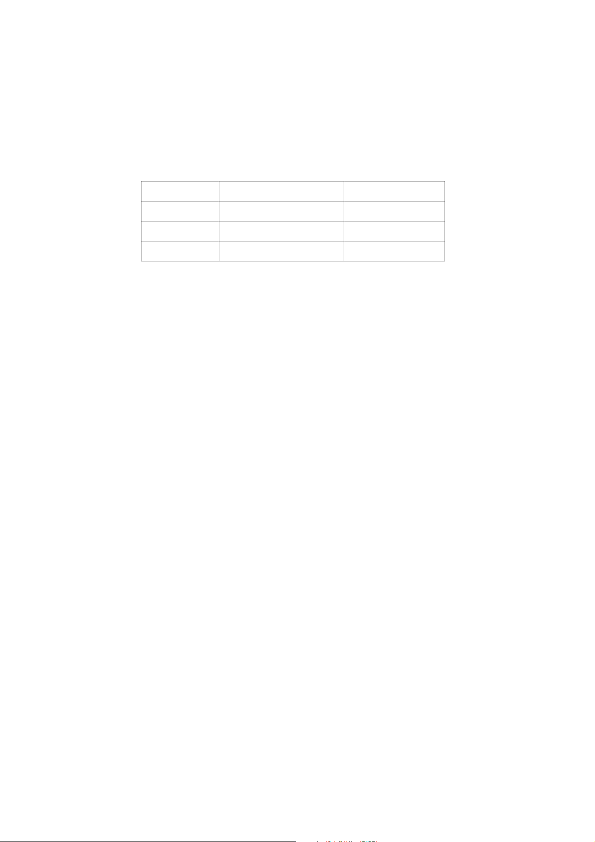
a) Test the pin voltage of P802/power board , the data is shown in table1:
Table1
voltage data of P802
P802 Pin1,2
Voltage
GND 22.8-25.2V
Pin3,4 Pin5,6,7
GND 11.4-12.6V 4.75-5.25V
For42”
Pin8,9 Pin10,11,12
On:2V-5.5V
Off: 0-0.5V
b) Test the pin voltage of P803/power board, the data is shown in table2:
Table2 voltage data of P803
P803 Pin1,2,3,4,5 Pin6,7,8,9,10
Voltage
22.8-25.2V GND NC 2V-5V 2.5-5V PWM NC
For42”
Pin11 Pin12 Pin13 Pin14
Pin13 Pin14 Pin15 Pin16
<0.6V
2.5-5V
PWM
2-5V
5
Page 6
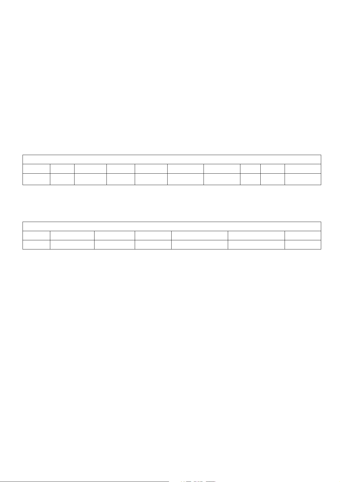
2.3. Alignment flow-chart
The alignment flow-chart is shown as fig-1
Connect to the center signal source and check each
Function of TV (station leaking, analog control, etc.)
Check the output of earphone and speaker.
Check if DDC, HDCP KEY, FLASH are written
Combined test for general assembly
White balance adjustment
Input AV/SVIDEO signal and check the function
Input HD signal and check the function of YPbPr
Input VGA signal and check if the display is normal, check
the function (analog control), horizontal/vertical center, etc.
Input HDMI signal and check if the display is normal, check
the function (analog control), horizontal/vertical center, etc.
Preset ex-factory
Check the accessories and packing
Fig-1 adjustment flow-chart
6
Page 7

2.4. Adjustment instruction
At any input source then press the remote controller buttons “<”, “EXIT” and “>” to enter factory mode.
During Factory menu, if “MENU” or “EXIT” key is pushed, system will exit factory mode.
2.4-1. Source Calibration
4-1.1. Set the TV input source to YPbPr; ASTRO-859 signal setting to PG2 program number 933(1080i).
(PG2 mode Timing 933 and Pattern 924 100% Color Bar.)
4-1.2. Entering into factory Mode: Press up or down key of remote control to select “Auto Calibration”, Press
「OK」 key to start.
-> Source calibration performed automatically when finished that will show OK.
7
Page 8

4-1.3. Change input source to PC.
Change Astro-859 Timing to No.953 (640x480@60Hz) and pattern on 953(8step V-grayscale).
Repeat step 4-1.2 to do source calibration,
2.4-2. Color Temperature Adjustment & Check
4-2.1. Set input source.
Set the signal generator Astro-859 timing to PG2-924 on Video & YPbPr, PG2-860 on HDMI, and PG2-963
on PC. Pattern sets 956 on all of the source.
Then press Astro-859 “FORMAT” key and key, then adjust RGB value to R:204, G:204, B:204
8
Page 9
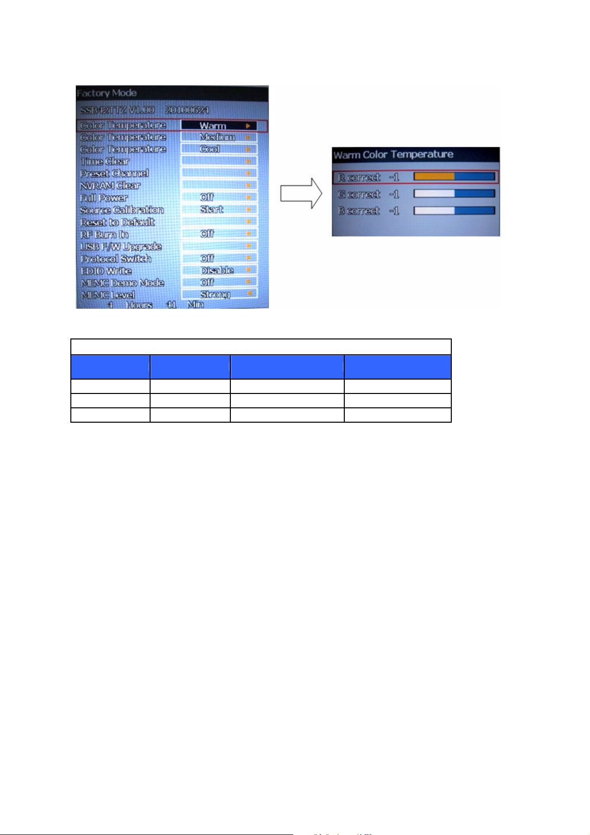
4-2.2. In factory mode OSD menu, select “Color Temperature” item, press “OK” key to enter the item.
R, G, B drive values are set for Warm, Medium, and Cool independently.
4-2.3. Set Color Temperature for “Warm”, “Medium” and “Cool” with following spec table.
Color temperature(for 42")
Color Temp. Cool Medium Warm
x 0.267
y 0.271
Tolerance ± 0.01
0.281
0.288
± 0.01
If the x and y value are larger than specification,
Decrease Red drive from default value.
Increase Blue drive from default value.
If the x or y or both x and y value is/are smaller than specification.
Decrease Blue drive from default value
According to a x and y value, please following adjustment of 1 or 2.
1 If x value is higher than spec
Decrease Red drive from default value.
2 If y value is higher than spec,
Increase Blue drive from default value
4-2.4 Exit Factory Mode:
After finishing adjusting color temperature, press [MENU] or [EXIT] to exit factory mode.
0.301
0.310
± 0.01
9
Page 10
2.5. Items of Factory menu
Vendor may customize design and add adjustment items Factory menu as far as all required items are
included.
Press up and down key can move high light item from Color Temperature Warn -> Color Temperature
Medium -> Color Temperature Cool ->Preset Channel-> Source Calibration -> Reset to Default.
The NVRAM Clear and Reset to Default items will have a check dialog “YES” and “NO” to do or not.
Push “Enter” key can select high light item function. (Press left and right can adjust value)
Display model name, firmware version and released date on top.
10
Page 11

5-1) Color Temperature for Warm
Press up or down key can select high light item function.
Press enter key to enter the item.
Following data for color temp shall be edited manually.
-R, G, B data for each preset.
-Press “Up” or “Down” key to select “R”, “G”, “B” item
-Press “Left” or “Right” key to set the “R”, “G”, “B” value.
-Press “MENU” or “EXIT” item to exit to factory mode
5-2) Color Temperature for Medium
Press up or down key can select high light item function.
Press enter key to enter the item.
Following data for color temp shall be edited manually.
-R, G, B data for each preset.
-Press “Up” or “Down” key to select “R”, “G”, “B” item
-Press “Left” or “Right” key to set the “R”, “G”, “B” value.
-Press “MENU” or “EXIT” item to exit to factory mode
5-3) Color Temperature for Cool
Press up or down key can select high light item function.
Press enter key to enter the item.
Following data for color temp shall be edited manually.
-R, G, B data for each preset.
-Press “Up” or “Down” key to select “R”, “G”, “B” item
-Press “Left” or “Right” key to set the “R”, “G”, “B” value.
-Press “MENU” or “EXIT” item to exit to factory mode
5-4) Time Clear
Press up or down key can select high light item function.
Press “Left” & “Right” key to select the item.
The timer on bottom is to record power on time for panel life.
It was set one time on production only.
5-5) Preset Channel
This is for factory to do some tests.
5-6) NVRAM Clear
Initialize program’s default values to NVRAM for following adjustment items accuracy.
In factory mode it is the first and important step to make sure all values are default value and correct.
- Reset settings: Channel table, Mode table (H/V Position, Clock, Phase), Source dependent setting
(Contrast, Brightness etc.), Common setting (Volume, Language etc.), Parental Control (Rating,
Password etc), Closed Caption.
To avoid a mistake initial process after factory setting is done. This item will have a check dialog to do the
initial or not.
NOTICE:
After this item is processed, the DUT needs to be powered off then AC powered off.
5-7) Full Power
This is for power consumption testing.
To measure the maximum power consumption of TV set, we adjust the value of following items to maximum.
11
Page 12

- Video: Contrast maximum value, Brightness maximum value, Backlight maximum value.
- Audio: Volume maximum value.
Press right key to turn on Full Power and OSD stay display until press enter key to recover from Full Power.
5-8) Source Calibration
Auto Calibration (gain/offset) must be adjusted color by firmware automatic adjustment in PC, and
Video3(Component) input source.
This item will have a result dialog “OK” or “NG”.
5-9) Reset to Default
This function is same as “NVRAM Clear”, but it will power off automatically after processing this function.
5-10) RF Burn In
Use “snow” pattern for burn in. Selected items are “On” and “Off”.
While turn on burn in mode, firmware will automatically turn off “Auto power off” function.
If there is no power supply suddenly, firmware will re-enter burn in mode automatically
when power supply is back.
Pressed the “Power” key, firmware will automatically turn off burn in mode.
- Burn in mode: Source is “TV”, Input Configuration is “Antenna” and channel is NTSC channel 2.
5-11) USB F/W Upgrade
The function is using USB device to upgrade firmware via USB port.
Copy the firmware file to USB device root path.
Execute this function to update firmware, the following OSD will display.
Note: After finishing updated, the system will reboot automatically
5-12) Protocol Switch
This is for debugging only. It is no use for service.
5-13) EDID Write
This is for writing EDID on the VGA source.
12
Page 13

5-14) MEMC Demo Mode
To separate screen into two parts that left side is 60Hz and right side is 120Hz for display.
5-15) MEMC Level
Changing MEMC level to Weak, Medium or Strong.
2.6. Performance check
No
Signal
name
Table4
Signal mode
Resolution
YPbPr
frequency(Hz)
signal format
Vertical
Horizontal
frequency
(KHz) (MHz)
Dot clock
frequency
Remarks
6-1 TV function
Connect RF to the center signal source, enter Channel menu → Channel Scan, check if there are channels be
skipped, check if the picture and speaker are normal.
6-2 AV/S-Video terminals
Input AV/S-Video signal, check if the picture and sound are normal.
6-3 YPbPr/YCbCr terminal
Input YPbPr signal (VG-859 signal generator), separately input the YUV signals listed in table4 and check if
the display and sound are normal at any situation (power on, channel switch and format convert, etc.)
1
2
3 720P/60
4 1080i/60 1920x1080 60 33.75 74.25
480i 720x480 59.94 15.73 27
480P 720x480 59.94 31.47 27
1280x720 60 45 74.25
6-4
PC(
VGA) terminal
Input
PC(V
GA) signal (VG-859 signal generator), separately input the signals listed in table5 and check the
display and sound. If the image is deflection of the Horizontal and Vertical, select Menu->PC->Auto Adjust to
perform auto-correct.
Signal mode
No
Signal
name
1
VGA 640 x 480
2 SVGA 800 x 600
3
XGA 1024 x 768
Resolution
Table5
PC
signal format
Horizontal
frequency
Vertical
frequency(Hz)
59.941 31.469 25.175
60.317 37.879 40
60.004 48.363 65
(KHz) (MHz)
Dot clock
frequency
Remarks
4
W-XGA
5
6 SXGA 1280 x 1024
1280 x 768
1360 x 768
59.87 47.776 79.5
60.015 47.712 85.5
60.02 63.981 108
13
Page 14
6-5 HDMI terminal
Input HDMI signal (VG-859 signal generator), separately input the signals listed in table6 and check the display
and sound (32KHz, 44.1KHz, 48KHz) at any situation (power on, channel switch and format convert, etc.)
Table6
HDMI
signal format
No
1
2
3
Signal mode
Signal
name
VGA 640 x 480 59.94 31.469 25.175
SVGA 800 x 600 60.317 37.879 40
XGA 1024 x 768 60.004 48.363 65
Resolution Vertical frequency(Hz) (KHz) (MHz)
Horizontal
frequency
Dot clock
frequency
Remarks
4
W-XGA
5
6
SXGA 1280 x 1024
7
8
9 720P/60
10 1080i/60 1920x1080 60 33.75 74.25
11 1080p/60 1920x1080 60 67.5 148.5
12 1080p/24 1920x1080 24 27 74.25
480i 720x480 59.94 15.734 27
480P 720x480 59.94 31.5 27.03
1280 x 768 59.87 47.776 79.5
1360 x 768 60.015 47.712 85.5
60.02 63.981 108
1280x720 60 45 74.25
6-6 other functions check
a) Check the turn on/turn off timer, sleep timer, picture/sound mode, OSD, stereo and analog TV Close Caption, V-
Chip, etc.
14
Page 15

3. Working principle analysis of the unit
1. NTSC/ATSC signal flow:
Antenna reception NTSC/ATSC signal will be send to tuner U32,
demodulating and output
These
differential IF+ IF- signal
interlace and scaler, then output LVDS level drive for panel display.
The
differential signals
amplifying, bass adjusting and volume control, the sound signal will
I2 S s i g na l b y
scaler
2. AV/S-VIDEO signal flow
S-VIDEO & Video path AV signal switch
differential IF+ IF- signal .
will send to the master control IC U1 to video/MPEGII decode, de-
will be fed into U1 to demodulate audio signals , after demodulating, pre-
I C
and sent to digital amplifier U5 amplifying,
by menu “Inpput list”
t h e n T u n e r w il l b e
b e t r a ns f or m i nt o d ig i t a l
then output to speaker.
via terminal socket, the signal and
the Video2 path AV signal will be fed to U1 to perform video decode, de-interlace and scaler, then
output LVDS drive level for panel display.
Audio signal from AV
the sound signal will be
amplifying,
output to speaker.
3. PC/YPrPb signal flow
terminal
via matched resistance is fed to U1 to bass adjust and volume control,
transfered into digital I2S signal by scaler IC
and sent to digital amplifier U5
PC and the Video2 path YPbPr signal are via terminal sent to U1 A/D conversion, output R/G/B of
24 bit to back end module to digital decode, image scale, then send to LVDS level drive for panel
display.
Sound signal of PC/YPrPb
te r m i n a l
via matched resistance
an d
sent to U1 to bass adjust and
volume control, the sound signal will be transform into digital I2S signal by scaler IC and sent to digital
amplifier U5 amplifying,
4. HDMI signal flow
HDMI video signal via terminal sent to
level for panel display. HDMI audio signal via decoder built-in terminal sent to
to bass adjust and volume control, the sound signal will
scaler IC and sent to digital amplifier
then output to speaker.
U1
U5
amplifying,
to digital decode, image scale, then output LVDS drive
U1 is
be
transform into digital I2S signal by
fed to back end
then output to speaker.
5. MEDIA signal flow
The JPEG file via USB terminal send to U1 to MPEG decode , image scale , then output LVDS
drive level for panel display .
15
Page 16

4. Block diagram-SANYO 42” ATSC model System Diagram
IR / LED Board
Light Sensor
42" MEMC
Main Board
HDMI 2
HDMI 1
Flash
MXIC
MX25L3205DM2I
PC
PC audio
DDRII 512M
Samsung
K4T51163QG-HCF7
DTV system IC
RENESAS
DTV-C7
R8J66977BG
S_Video
Composite
Y
Component
PrPb
Panel out
LVDS out
Audio I2S output
Digital audio out
(Coaxial)
Audio
AMP
ST
STA335W
DRV602PW
audio Line Out
IF +/-
R_out
L-out
DTVA50CVH1019B
ANT / CABLE
Tuner
Samsung
Side
HDMI
USB
Keypad
16
Page 17

Block diagram-POWER-42”
17
Page 18

5.IC block diagram
5-1. Renesas R8J66975-RFJZ , R8J66977BG-RFJZ
Model - SubModel Surround Maximum panel size Number of HDMI ports
R8J66975BG-RFJZ Simple surround WSXGA+
(1680 x 1050)
R8J66977BG-RFJZ Simple surround FullHD
(1920 x 1080)
Features
Main CPU
32bit RISC Super-H architecture SH3 CPU core
Demodulator
ATSC A/53 compliant 8VSB receiver /w QAM.
IF AGC control interface x1ch
System decoder (Stream demultiplexer)
Video and audio ES stream filtering x1
Section filtering: max. 32 PIDs
MPEG video decoder
Single ISO-13818-2 MP@ML or MP@HL support
Supports decoding of all ATSC-compliant formats
JPEG decoder
Decode Base-line JPEG file
2D Graphics
CEA-608/CEA-708-B closed caption support
Display processor, Video input/output
Full 10bit processing
MPEG Noise Filter (De-blocking/De-ringing)
Over Drive (Panel resolution : up to WXGA)
Inputs : CVBS x3, Y/C x2, YPbPr x2, RGB x1, HDMI x3
Outputs : 10-bit dual LVDS
Audio decoder, Audio input/output
ATSC A/52 Clear QAM compliant audio decoding support
Sound Demodulator
Inputs : SIF x1, Stereo x6
Outputs : PCM (I2S) x2, S/PDIF x1, Stereo x1
Peripheral interfaces
UART x1, Legacy serial interface x2, USB High Speed x1
General purpose I/Os
Memory interfaces
Serial Flash
16b width DDR2 800Mbps(5-5-5) SDRAM x 1
Power, clock and package
1.26(±0.06)V, 1.82(±0.08)V, 3.3(±0.15)V
25MHz X’tal
376pin PBGA
3
3
18
Page 19

5-2. Block diagram
19
Page 20

42” Block
20
Page 21

Wiring Connection
1
2
3
4
5
6
7
8
1
9
2
10
3
11
4
12
5
6
14
VTV-L42601 VTV-L42601 VTV-L42601 VTV-L42601 Power/B
CN1 CN3 CN15 CN2 P802
1 GND 1 LED Mute 1 VDD 21 GND 1 SPK_OUTR+ 1 GND
2 GND 2 LED Green 2 VDD 22 GND 2 SPK_OUTR- 2 GND
3 24V 3 LED Red 3 VDD 23 Panel SEL 3 SPK_OUTL- 3 24V
4 24V 4 GND 4 VDD 24 GND 4 SPK_OUTL+ 4 24V
5 GND 5 IR SENS 5 LV0OUT4M 25 LV1OUT4M 5 GND
6 GND 6 3.3V 6 LV0OUT4P 26 LV1OUT4P 6 GND
7 GND 7 Light Sensor 7 LV0OUT3M 27 LV1CKOM 7 GND
8 12V 8 5V 8 LV0OUT3P 28 LV1CKOP
9 12V 9 LV0OUT2M 29 LV1OUT3M
10 5V 10 LV0OUT2P 30 LV1OUT3P
11 5V 11 GND 31 LV1OUT2M
12 5V 12 GND 32 LV1OUT2P
13 Power ON 13 LV0CKOM 33 LV1OUT1M
14 AC OFF Detect 14 LV0CKOP 34 LV1OUT1P
15 BACKLIGHT_ADJ 15 GND 35 LV1OUT0M 15 BL_ADJ
CN16 8 12V
MEMC SEL 0 9 12V
SIDA1 10 5V
MEMC SEL 1 11 5V
SICL1 12 5V
FR Select 13 Power ON 13 BL_ADJ
GND 14 ACD
P803
24V
24V
24V
24V
24V
GND
GND
GND
GND
GND
NC
BL_EN
NC
16 BACKLIGHT_EN 16 GND 36 LV1OUT0P 16 BL_EN
17 LV0OUT1M 37 GND
18 LV0OUT1P 38 DCR EN
19 LV0OUT0M 39 BACKLIGHT_ADJ
20 LV0OUT0P 40 DCR ADJ
21
Page 22

7. Trouble Shooting
7-1. Fault clearance
22
Page 23

7-2. Troubleshooting guide
The flow chart shown below will help you to troubleshoot your Televison set with it doesn’t display
normally. Each procedure offers a simple way to check for system errors. Before starting, ensure
that there is a signal in and that the Televison is turned on.
7.2-1 Power LED no light
Change to new power board.
P /N : P K101V2010I (SSB42T)
23
Page 24

7.2-2 Has audio but no video out
Change to new power board.
P /N : P K101V2010I
(
SSB42T)
24
Page 25

7.2-3 Has video but no audio out
Have a video but no
sound
Check volume or
Mute
OK
Check Input
source
OK
Check speaker Change speaker
OK
MUTE
NG
NG
Cancel mute function
Or adjust volume up
Change source device
Change main pcb
25
Page 26

Change to new power board.
P /N : P K101V2010I (SSB42T)
26
Page 27

8.SCHEMATIC DIAGRAM
ELECTRON-42"
Page 28

5
Sheet Index
Page 03 - System Power
4
3
2
MAIN PCB1
MAIN PCB1
1
FW1
FW1
FIRMWARE
FIRMWARE
FW STC40T REV1.0
FW STC40T REV1.0
Page 04 - C7 & MCU / Key
D D
Page 05 - C7 & Tuner Input
EMIcover1
EMIcover1
Page 06 - C7 & Video Input
Page 07 - C7 & VGA Input
Page 08 - C7 & HDMI Input
Page 09- C7 & Audio Input
Page 10 - C7 & Debug IO / FLASH ROM
EMIcover-C7
EMIcover-C7
Page 11- C7 & Power
Page 12 - C7 & DDRII-800
Page 13 - C7 & LVDS Output
Page 14 - C7 & Audio Out
C C
Page 15 - Audio Amplifier
VTV-L40601 REV:0A
VTV-L40601 REV:0A
Notice
1. All Res. is 0603.
2. All Cap. is 0402 (<=0.47uF), 0603 (<=1uF), 0805 (<=10uF).
0402
NPO 5pF/50V, 10pF/50V, 22pF/50V, 27pF/50V, 33pF/50V, 36pF/50V, 47pF/50V, 220pF/50V
X7R 100pF/25V, 470pF/25V, 1000pF/25V, 2200pF/25V, 3300pF/25V, 0.01uF/25V, 0.01uF/50V, 0.022uF/25V
X5R 1uF/10V
Y5V 0.1uF/25V, 0.33uF/10V, 0.47uF/10V
B B
0603
Y5V 0.1uF/50V, 0.47uF/25V, 1uF/16V
X5R 10uF/6.3V
0805
X5R 4.7uF/16V
Y5V 0.47uF/50V, 0.68uF/50V, 1uF/50V, 3.3uF/10V, 10uF/10V
1206
Y5V 4.7uF/35V
1210
Y5V 10uF/35V
A A
3. The mark "#" to indicate that Part disuse.
Renesas Scaler
5
COMPAL OPTOELECTRONICS CO., LTD
COMPAL OPTOELECTRONICS CO., LTD
COMPAL OPTOELECTRONICS CO., LTD
Title
Title
Title
SCHEMATIC,M/B VTV-L42601,SSB42T
SCHEMATIC,M/B VTV-L42601,SSB42T
SCHEMATIC,M/B VTV-L42601,SSB42T
Size Document Number Rev
Size Document Number Rev
Size Document Number Rev
A4
A4
A4
Date: Sheet of
Friday, June 04, 2010
Date: Sheet of
Friday, June 04, 2010
Date: Sheet of
4
3
Friday, June 04, 2010
2
401C2K
401C2K
401C2K
2 15
2 15
2 15
1
1A
1A
1A
Page 29

5
R7 0R7 0
12
C49
C49
10uF/10V/0805/NC
10uF/10V/0805/NC
C0805D
C0805D
GND
G
GND
C330
C330
10uF/10V/0805
10uF/10V/0805
P5V
P5V
update for AC off
screen garbage
20100526
R368
R368
1K/0402
1K/0402
CE
R369 100/1% /0402R369 100/1% /0402
B
Q45
Q45
MMBT3904L
MMBT3904L
R20 30K/1%/04 02R20 30K/1% /0402
1 2
R4
2.2KR42.2K
47K
47K
B
47K
47K
12
0.1uF/50V/NC
0.1uF/50V/NC
GND
R297 10K/0402R297 10K/0 402
1 2
12
C69
C69
1uF/16V
1uF/16V
C0603D
C0603D
GND GND
Power Module Input
CN1
CN1
JWT A2001W V2-16P
JWT A2001W V2-16P
1
2
3
4
5
6
7
8
9
10
D D
11
12
13
14
15
16
GND
C C
Standby Power
P5V
FB10
FB10
KHB0603N121SA
KHB0603N121SA
C329
C329
10uF/10V/0805
10uF/10V/0805
B B
L1 B201212K800TM
L1 B201212K800TM
L0805D
L0805D
P24V P_DA MP
1 2
L2 B201212K800TM/NC
L2 B201212K800TM/NC
L0805D
L0805D
1 2
POWER_O N2
PG
BKLT_EN
12
R9
10K/0402R910K/0402
GND
RTX update for power
shut down issue 20091231
R221 10K/ 1%/NCR221 1 0K/1%/NC
C318
C318
0.1uF/10V/0402
0.1uF/10V/0402
GND
R308
R308
10K/1%
10K/1%
U43
U43
GND
G9141T11U
G9141T11U
3
/SHDN
OUT
1
IN
SET
GND
2
GND G ND
P_DAMP
P12V
P5V
POWER_O N2 4
12
R10
R10
100K/0402
100K/0402
GND
P5V
R367
R367
560
560
D
C425
C425
10uF/10V/0805
10uF/10V/0805
S
GNDGND
Q44
Q44
MMBT3409L(2N7002E)
MMBT3409L(2N7002E)
3.3V_STB
5
R242
R242
4
RTX update for power
shut down issue 20091231
C197
C197
23.2K/1%
23.2K/1%
R307
R307
0.1uF/10V/0402
0.1uF/10V/0402
10K/1%
10K/1%
POWER_O N1
POWER_O N14
Frank update for DC
power on fail issue
20100202
LCD PANEL POWER MosFET
GND
5
12
R193KR19
3K
GND
12
C66
C66
10uF/10V/0805
10uF/10V/0805
C0805D
C0805D
P5VP12V
12
1 2
R39
R39
24K
24K
12
R18
R18
0/1206/NC
0/1206/NC
R1206D
R1206D
12
C75
C75
1uF/16V/NC
1uF/16V/NC
C0603D
C0603D
B
GND
R280R28
0
1 2
CE
MMBT3904LQ2MMBT3904L
U7
APM4461U7APM4461
1
8
S1
D4
2
7
S2
D3
3
6
S3
D2
5
G4D1
12
R22
R22
1K/1206
1K/1206
R1206D
12
GND
Q2
R1206D
GND
C70
C70
1uF/16V/NC
1uF/16V/NC
C0603D
C0603D
Vds = -24V
Vgs = -2.5V/-4.5V/-10V
Id = -2A/-4A/-7A
(APM4461)
1 2
12
R17
R17
0/1206
0/1206
R1206D
R1206D
+
+
GND
A A
PANEL_VEN
PANEL_VEN4
C65
C65
C58
C58
0.1uF/50V
0.1uF/50V
SE100uF/16V
SE100uF/16V
RTX update for panel
sequence 20100226
R25 22KR25 22 K
1 2
12
R26
R26
5.6K
5.6K
GND
3.3V_STB
R13
R13
22K
22K
ACOFF_DET
Q38
Q38
PDTC114ET
PDTC114ET
E C
GND
R8 0R8 0
1 2
1K/1%/0402/NC
1K/1%/0402/NC
R36 1K/1%/0402/NCR 36 1K/1%/0402/NC
C72
C72
MMBT3904L/NC
MMBT3904L/NC
R370
R370
10K/0402/NC
10K/0402/NC
GND
Q48
Q48
APM2301AAC
APM2301AAC
G
CE
Q3
B
MMBT3904LQ3MMBT3904L
L14 B201212K800TM
L14 B201212K800TM
L0805D
L0805D
COLLECTOR
DTC124EK
SOT-23B
BASE
4
D9
1N4148D91N4148
1 2
BKLT_EN
3.3VD
R35
R35
12
Q46
Q46
GND
BACKLIGHT_EN 4
L17
L17
B201212K800TM
B201212K800TM
L0805D
L0805D
1 2
DS
VDD_LCD
12
C57
C57
0.1uF/50V
0.1uF/50V
GND
EMITTER
4
ACOFF_DET 4
update for power team
standby 5V hold time
20100526
3.3V_STB
R330
R330
10K/1%/NC
10K/1%/NC
1 2
R32
R32
CE
1K/1%/NC
1K/1%/NC
B
1 2
12
GND
12
C71
C71
10uF/10V/0805
10uF/10V/0805
C0805D
C0805D
GND GND GND
VDD_LCD
R11 0R11 0
1 2
R12 0/NCR12 0/NC
1 2
C67
C67
100pF/25V/0402/NC
100pF/25V/0402/NC
12
C78
C78
10nF/25V/0402
10nF/25V/0402
RTX update for DC
power on fail
20100225
BACKLIGHT_ADJ 4,13
DCR_ADJ 13
3.3VD
12
C86
C86
0.1uF/10V/0402
0.1uF/10V/0402
3
DC - DC FROM VCC TO 1.25V(2A)
P5V
KHB0805W121S A_6A
KHB0805W121S A_6A
FB68
5V -> 1.8V
P5V
+
+
5V -> 3.3V
POWER_O N14
C196
C196
SE100uF/16V
SE100uF/16V
FB68
10uF/10V/0805
10uF/10V/0805
3.3VA
3.3VD
12
C50
C50
0.1uF/10V/0402
0.1uF/10V/0402
GND
C372
C372
POWER_O N1
3
GND GND
R45 10K/1%0402/NCR45 10K/1%0402/NC
R24 10K/1%0402R24 10K/1%0402
P5V
1 2
1 2
20K/1%/0402/NC
20K/1%/0402/NC
1 2
1.25VD
R18210R182
C379
C379
0.1uF/10V/0402
0.1uF/10V/0402
C378
C378
0.1uF/10V/0402
0.1uF/10V/0402
R40
R40
1 2
GND
R15 10K/0402R 15 10K/0402
C41
C41
1uF/16V
1uF/16V
C0603D
C0603D
GND GND
12
C74
C74
1uF/16V
1uF/16V
C0603D
C0603D
GND
R93 9.09K/1%/0402R93 9.09K/1 %/0402
1 2
R95
R95
9.09K/1%/0402
9.09K/1%/0402
1 2
GND
12
GND
R94 9.09K/1%/0 402R94 9.09K/1%/0402
1.25VD
GND
10
GND
12
C43
C43
0.1uF/10V/0402
0.1uF/10V/0402
GND
APM2301AAC
APM2301AAC
R296 10K/0402R296 10K/0402
1 2
B
12
12
R96
R96
10K/NC
10K/NC
C73
C73
C0603D
C0603D
1uF/16V
1uF/16V
1 2
R97
R97
9.09K/1%/0402
9.09K/1%/0402
1 2
10uF/16V/0805
10uF/16V/0805
GND
12
12
R98
R98
10K/NC
10K/NC
8
1
5
G
CE
5
6
7
8
C192
C192
1uF/16V
1uF/16V
C0603D
C0603D
Q47
Q47
C434
C434
U2
G5694U2G5694
VIN
LX
VCC
FB
EN
REF
PGND
GND
THEM_PAD
6
3
9
GND GND
P5V_SW
DS
C32
C32
+
+
SE100uF/16V
SE100uF/16V
GND
Q1
MMBT3904LQ1MMBT3904L
U6
G9731F11UU6G9731F11U
VO
VIN
VO
VPP
ADJ
POK
GND
VEN
ThPad
9
GND
U8
G9731F11UU8G9731F11U
5
VIN
6
VPP
7
POK
8
VEN
ThPad
9
12
GND
C317
C317
1uF/16V
1uF/16V
C0603D
C0603D
GND
C413
C413
0.1uF/50V
0.1uF/50V
GND
FOR TUNER
L28 2.2uH /3.8AL28 2.2uH /3.8A
7
C347 47pF /50V/0402C347 47pF/50V/04 02
4
R355 9.09K/1%R355 9.09K/1%
2
R354 16K/1 %R354 16K/1%
C191
C191
0.1uF/10V/0402
0.1uF/10V/0402
Vout=0.8Vx (1+R1/R2)
U3 G1117-3.3V-252U3 G1117-3.3V-252
3
Vin
12
C34
C34
0.1uF/10V/0402
0.1uF/10V/0402
GND
4
3
R100
R100
2
12.7K/1%
12.7K/1%
1
1 2
R101
R101
10K/1%
10K/1%
1 2
GND
4
VO
3
VO
2
ADJ
1
GND
U31
U31
SSD9117-5.0V-252
SSD9117-5.0V-252
VIN3VOUT
ADJ / GND
1
10uF/10V/0805
10uF/10V/0805
1 2
1 2
GND
2
C436
C436
2
1.25VD
C356
C356
PVM330uF/6V
PVM330uF/6V
GND GND
2
Vout
C35
C35
+
+
ADJ/GND
SE100uF/16V
1
GND
1.8A
+
+
GND GND GND
R106
R106
12.7K/1%
12.7K/1%
R103
R103
10K/1%
10K/1%
SE100uF/16V
GND
Frank update for video source
horizontal and water wave nois e
issue 20100401
12
C51
C60
C60
SE100uF/16V
SE100uF/16V
5VSW
1 2
C415
C415
0.1uF/10V/0402
0.1uF/10V/0402
C51
10nF/25V/0402
10nF/25V/0402
12
10nF/25V/0402
10nF/25V/0402
L71 B20 1212K800TM
L71 B20 1212K800TM
L0805D
L0805D
C52
C52
PVM330uF/16V
PVM330uF/16V
1.8D
+
+
GND GND GND
2
12
C36
C36
10nF/25V/0402
10nF/25V/0402
GND
12
B201212K800TM/NC
B201212K800TM/NC
C59
C59
C53
C53
0.1uF/10V/0402
0.1uF/10V/0402
L0805D
L0805D
12
5VSW_CP12V
12
C37
C37
0.1uF/10V/0402
0.1uF/10V/0402
GND
L68
L68
1 2
1 2
C61
C61
0.1uF/10V/0402
0.1uF/10V/0402
L7 B201212K800TM
L7 B201212K800TM
L0805D
L0805D
1 2
12
L69
L69
B201212K800TM/NC
B201212K800TM/NC
L0805D
L0805D
L13 B20 1212K800TM
L13 B20 1212K800TM
L0805D
L0805D
1 2
L67 B201212K800TM
L67 B201212K800TM
L0805D
L0805D
1 2
L15 B20 1212K800TM
L15 B20 1212K800TM
L0805D
L0805D
1
12
C38
C38
10uF/10V/0805
10uF/10V/0805
C0805D
C0805D
recover as a bead
20100401
12
C62
C62
10uF/10V/0805
10uF/10V/0805
C0805D
C0805D
Title
Title
Title
Size Document Num ber Rev
Size Document Num ber Rev
Size Document Num ber Rev
A2
A2
A2
Date: Sheet of
Date: Sheet of
Date: Sheet of
3.3VA
12
C39
C39
10nF/25V/0402
10nF/25V/0402
GND GNDGND
12
GND GND GN DGND
12
C186
C186
10uF/10V/0805
10uF/10V/0805
C0805D
C0805D
COMPAL OPTOELECTRONICS CO., LTD
COMPAL OPTOELECTRONICS CO., LTD
COMPAL OPTOELECTRONICS CO., LTD
SCHEMATIC,M/B VTV-L42601,SSB42T
SCHEMATIC,M/B VTV-L42601,SSB42T
SCHEMATIC,M/B VTV-L42601,SSB42T
Friday, June 04, 2010
Friday, June 04, 2010
Friday, June 04, 2010
C54
C54
10uF/10V/0805
10uF/10V/0805
C0805D
C0805D
12
C376
C376
10nF/25V/0402
10nF/25V/0402
12
C63
C63
10nF/25V/0402
10nF/25V/0402
12
1.8VIF
1.8VD
401C2K
401C2K
401C2K
1
1.8VA
C55
C55
10nF/25V/0402
10nF/25V/0402
GNDGNDGND
12
C40
C40
0.1uF/10V/0402
0.1uF/10V/0402
12
C346
C346
0.1uF/10V/0402
0.1uF/10V/0402
GNDGNDGND
12
C64
C64
0.1uF/10V/0402
0.1uF/10V/0402
3.3VA
12
C56
C56
0.1uF/10V/0402
0.1uF/10V/0402
3 15
3 15
3 15
1.8VA
1.8VIF
1.8VD
1A
1A
1A
Page 30

5
3.3V_STB
PANEL_SEL
DAMP_RESETN
3.3V_STB
R31
R31
R30
R30
10K/0402
10K/0402
56K/0402
56K/0402
R0402D
R0402D
R0402D
R0402D
1 2
1 2
3.3V_STB
12
R41
R41
10K/0402
10K/0402
R0402D
R0402D
12
R315
R315
10K/0402
10K/0402
12
R42
R42
10K/0402
10K/0402
12
GND
C7 MCU
RTX update for DC
power on fail
20100130
MEMC_SEL_113
FR_SELECT13
D D
C C
B B
Check
DAMP_RESETN15
PANEL_SEL13
PC_HSYNC7
PC_VSYNC7
ACOFF_DET3
POWER_O N23
CUT_LEAK11
POWER_O N13
HDMI_CEC_C78
HDMI_HPD08
HDMI_HPD18
HDMI_HPD28
Keypad
R56 11K/1%R56 11K/1%
1 2
SW PUSH /4P/90D/1.3MM
SW PUSH /4P/90D/1.3MM
2
3
GND
GND
SW1
SW1
4
1
MENU VOL+VOL- CH+INPUT/EXIT CH- POWER
R57 6.19K/1%R57 6.19K/ 1%
1 2
SW PUSH /4P/90D/1.3MM
SW PUSH /4P/90D/1.3MM
2
3
GND
GND
SW2
SW2
4
1
3.6K/1%
3.6K/1%
R58
R58
1 2
SW PUSH /4P/90D/1.3MM
SW PUSH /4P/90D/1.3MM
2
3
GND
GND
SW3
SW3
4
1
R59 2.7K/1%R59 2.7K/1%
1 2
SW PUSH /4P/90D/1.3MM
SW PUSH /4P/90D/1.3MM
2
3
GND
GND
SW4
SW4
4
1
4
12
R37
R37
10K/0402
10K/0402
GND
KEY_POWER
PC_HSYNC
PC_VSYNC
ACOFF_DET
CUT_LEAK
POWER_O N1
HDMI_CEC_C7
IR_SENS
LED_COLOR
LED_R
HDMI_HPD0
HDMI_HPD1
HDMI_HPD2
R43
R43
1K/0402
1K/0402
update for LED
abnormal during
initial 20100112
GND
R60 1.8K/1%R60 1.8K/1%
1 2
SW PUSH /4P/90D/1.3MM
SW PUSH /4P/90D/1.3MM
2
3
GND
GND
SW5
SW5
4
1
U1A
U1A
R8J66977BG
R8J66977BG
BGA1090-1
BGA1090-1
W20
GPIO0
Y22
GPIO1
U19
GPIO2
V20
GPIO3
W21
GPIO4
W22
GPIO5
V21
GPIO6
M21
GPY05
M19
GPY06
N21
GPY07
L21
GPY08
L19
GPY09
L22
GPY10
K20
GPY11
K22
GPY12
K21
GPY13
L20
GPY14
K19
GPY15
J20
GPY16
J19
GPY17
J22
GPY18
P18
MODE0
1 2
R61 1.33K/1%R61 1.33K/ 1%
SW PUSH /4P/90D/1.3MM
SW PUSH /4P/90D/1.3MM
2
3
GND
GND
SW6
SW6
4
1
SCIRXD0
SCITXD0
SCIF0CSIO0
SCIF0CSIO0
SMDATA
SCISCK1
SCITXD1
SCIRXD1
SCIF1 CASIF
SCIF1 CASIF
MCU ADC
MCU ADC
BLC
BLC
12
R52
R52
10K/0402
10K/0402
KEY_IN0 KEY_POWER
SCLK0
STXD0
SRXD0
SMCLK
SMRST
MADIN0
MADIN1
MADIN2
MADIN3
MADIN4
MADIN5
MADIN6
MADIN7
QBLCA
QBLCB
W18
Y10
AB10
AA10
AA19
AB19
AA18
Y19
AA20
AB20
H19
G21
G20
H21
G22
H22
H20
J21
W17
Y17
PC_DET
BACKLIGHT_EN
PANEL_VEN
DAMP_PDN
INT_LINE
EDID_WPC
KEY_IN0POWER_O N2
Light_Sensor
LINE_MUTE
BACKLIGHT_ADJ
12
R376
R376
10K/0402
10K/0402
PWM_LED
12
R319
R319
10K/0402
10K/0402
GND
3.3V_STB3.3V_STB
SW PUSH /4P/90D/1.3MM
SW PUSH /4P/90D/1.3MM
2
3
GND
GND
SW7
SW7
4
1
AV1_S_DET
AB22
SCISCK0
AB21
12
R377
R377
10K/0402
10K/0402
R44 0/0402R44 0/0402
BACKLIGHT_ADJ 3,13
12
R53
R53
10K/0402
10K/0402
3
3.3V_STB
12
R318 10K/0402R318 10K/0402
R314 10K/0402/NCR314 10K/0402/NC
R316 10K/0402/NCR316 10K/0402/NC
12
12
AV1_S_DET 6MEMC_SEL_013
PC_DET 7
R38 0/0402R38 0/0402
12
BACKLIGHT_EN 3
DCR_EN 13
PANEL_VEN 3
DAMP_PDN 15
INT_LINE 15
EDID_WP 7
2
reserve for DCR
function 20100106
1
update for write protect 20091 211
12
12
R378
R378
10K/0402
10K/0402
12
R329
R329
10K/0402
10K/0402
12
R379
R379
10K/0402
10K/0402
12
12
R380
R380
R375
R375
10K/0402/NC
10K/0402/NC
1K/0402
1K/0402
RTX update for leakage
voltage 20100119
GND
LED_GREEN_C 7
12
R320
R320
1K/0402
1K/0402
update for LED
abnormal during
initial 20100112
GND
1206L035-CF21206L035-C
W/O LED Effect model--->8 pin connector
W/LED Effect model--->12pin connector
CN3
CN3
JWT A2001W V2-12P
JWT A2001W V2-12P
1
2
3
4
5
6
7
8
9
10
11
12
GND
100pF/25V/0402
100pF/25V/0402
L39 KHB06 03Q300SAL39 KHB0603Q300SA
1 2
PWM_LED
LED_color
C386
C386
100pF/25V/0402
100pF/25V/0402
TP22TP22
TP21TP21
LED_MUTE 3
LINE_MUTE 14
TP34TP34
IR & LED Connector
Light sensor Connector
P5V
12
L64
L64
B201212K800TM
B201212K800TM
L0805D
L0805D
R62
R62
18K/1%/0402
18K/1%/0402
12
F2
EZJZ1V80010D8EZJZ1V80010
D8
C388
100pF/25V/0402
C388
100pF/25V/0402
C385
C385
3.3V_STB
F3
F3
1206L035-C/NC
1206L035-C/NC
LED_GREEN_C 7
LED_R
IR_SENS
1 2
R102
R102
10K/1%
10K/1%
EZJZ1V80010
EZJZ1V80010
EZJZ1V80010
EZJZ1V80010
EZJZ1V80010
R63 30K/1%/040 2R63 30K/1%/0402
D13
D13
100pF/25V/0402
100pF/25V/0402
C387
100pF/25V/0402
C387
100pF/25V/0402
1 2
EZJZ1V80010
EZJZ1V80010
D16
D16
C335
C335
100pF/25V/0402
100pF/25V/0402
EZJZ1V80010
D17
D17
D18
D18
C336
C336
C339
100pF/25V/0402
C339
100pF/25V/0402
LED_MUTE 3
12
C348
C348
4.7uF/6.3V
4.7uF/6.3V
C0603D
C0603D
Light_Sensor
12
R105
R105
39K/1%
39K/1%
GND
GND GND
A A
5
4
3
GND
COMPAL OPTOELECTRONICS CO., LTD
COMPAL OPTOELECTRONICS CO., LTD
COMPAL OPTOELECTRONICS CO., LTD
Title
Title
Title
SCHEMATIC,M/B VTV-L42601,SSB42T
SCHEMATIC,M/B VTV-L42601,SSB42T
SCHEMATIC,M/B VTV-L42601,SSB42T
Size Document Num ber Rev
Size Document Num ber Rev
Size Document Num ber Rev
A2
A2
A2
Date: Sheet of
Friday, June 04, 2010
Date: Sheet of
Friday, June 04, 2010
Date: Sheet of
2
Friday, June 04, 2010
401C2K
401C2K
401C2K
1
4 15
4 15
4 15
1A
1A
1A
Page 31

TUNER & C7
5
4
Default Setting Samsung tuner
3
close to Tuner
5VSW
12
R67
R67
4.7K/0402
4.7K/0402
2
12
R65
R65
4.7K/0402
4.7K/0402
1
D D
SAMSUNG
U32
U32
DTVA50C VH1019B
DTVA50C VH1019B
1
1-NC
2
2-B+
3
3-NC
22
22
13-IF MOINTOR
21
21
C C
U10 ENV56 U03D8F
U10 ENV56 U03D8F
15
GND
16
GND
GND
17
GND
18
GND
B B
17171818191920
20
GND
RF AGC Monitor
BT Monitor
IF Monitor
Panasonic
ENV56U03D8F
Panasonic
ENV56U03D8F
Panasonic Samsung
R76
R75
C97
C102
L23
L26
C697
C696
L24
A A
C100
L3,L4 0 ohm
4
4-NC
5
5-GND
6
10-NC
11-SCL
12-SDA
14-IFAGC
15-IF2
16-IF1
SCL
SDA
IF AGC
IFD-out1
IFD-out2
NC
NC
6-NC
7-NC
8-NC
9-NC
+B
7
8
9
10
11
12
13
14
15
16
1
2
3
5
6
9
10
R77
R77
11
1K/1%/040 2/NC
1K/1%/040 2/NC
12
13
14
R74
R74
1K/1%/040 2/NC
1K/1%/040 2/NC
GND
12
12
0 ohm
0 ohm 75 ohm
10nF
10nF
0.22uH
0.22uH
NC
NC
0.1uH
120pF
0.27uH-->0ohm
IF+
IF-
75 ohm
47pF
47pF
0.27uH
0.27uH
NC
NC
0.27uH
39pF
close to Tuner
B201212 K800TM
B201212 K800TM
5VSW
12
L27
L27
B201212 K800TM
B201212 K800TM
L0805D
L0805D
C109 10uF/10V/0805C109 10uF/10V/0805
12
C108 0.1uF/10V/0402C108 0.1uF/10V/0402
1 2
L12
L12
L0805D
L0805D
1 2
1 2
TUN_SCL
TUN_SDA
close to tuner
R76 75R76 75
1 2
GND
R75 75R75 75
1 2
L16
L16
B201212 K800TM
B201212 K800TM
L0805D
L0805D
close to Tuner and Guard GND
R73 0/0 402R73 0/0 402
1 2
12
C95
C95
0.1uF/10V /0402/NC
0.1uF/10V /0402/NC
GND
close to C7
C97
C97
47pF/50V /0402
47pF/50V /0402
1 2
1 2
L23
L23
FLMA-201 209-R27KT
FLMA-201 209-R27KT
L24
L24
TDK MLF1 608DR27K
TDK MLF1 608DR27K
L26
L26
FLMA-201 209-R27KT
FLMA-201 209-R27KT
1 2
1 2
C102
C102
47pF/50V /0402
47pF/50V /0402
12
C697
C697
15pF/50V /0402/NC
15pF/50V /0402/NC
GND
22pF/50V /0402
22pF/50V /0402
update for ATV disorderly
20100417
12
12
C100
C100
39pF/50V /0402
39pF/50V /0402
12
C696
C696
15pF/50V /0402/NC
15pF/50V /0402/NC
R68
R68
100/1%/04 02
100/1%/04 02
1 2
12
C90
C90
GND
close to c7 and Guard GND
R71 1K/1 %/0402R71 1K/1%/04 02
1 2
12
C92
C92
0.33uF/10 V/0402
0.33uF/10 V/0402
GND GND
L3
0/0805L30/0805
1 2
1 2
L4
0/0805L40/0805
R69
R69
100/1%/04 02
100/1%/04 02
1 2
12
C91
C91
22pF/50V /0402
22pF/50V /0402
GND
12
1 2
C3 33 pF/50V/NCC3 33 pF/50V/NC
C4 33 pF/50V/NCC4 33 pF/50V/NC
1 2
R72 1K /1%/0402R72 1K/1%/0 402
1 2
C93
C93
0.1uF/10V /0402
0.1uF/10V /0402
GND
R352 10K/1%/0 402R352 10K/1%/0 402
1 2
R347 10K/040 2R34 7 10K/040 2
1 2
GND
12
C104
C104
0.1uF/10V /0402
0.1uF/10V /0402
GND GND
PCB Name-Rev : VTV-L40602-0A
U1B
U1B
R8J66977BG
R8J66977BG
BGA1090 -1
BGA1090 -1
K3
SICL0
K2
SIDA0
J1
IFAGC
L4
RFAGC
K1
SANT
E3
SIFIN
F2
IFINP
F1
IFINM
E2
VRPIF
12
C105
C105
E1
VRMIF
0.1uF/10V /0402
0.1uF/10V /0402
IIC0
IIC0
VSB
VSB
VSB / SIF ADC
VSB / SIF ADC
C3,C4 NC 33pF-->NC
Title
Title
Title
SCHEMAT IC,M/B VTV-L42601,SS B42T
SCHEMAT IC,M/B VTV-L42601,SS B42T
SCHEMAT IC,M/B VTV-L42601,SS B42T
Size Document N umber Rev
Size Document N umber Rev
Size Document N umber Rev
A3
A3
A3
401C2K
401C2K
401C2K
Date: Sheet of
Date: Sheet of
Date: Sheet of
5
4
3
2
5 15Saturday, June 19, 2 010
5 15Saturday, June 19, 2 010
5 15Saturday, June 19, 2 010
1
1A
1A
1A
Page 32

5
4
3
2
1
5VSW_C
CE
Q14
Q14
MMBT3904L
MMBT3904L
12
R110
R110
390
390
GND
SPDIF 14
L80 KHB0603 Q300SA
L80 KHB0603 Q300SA
1 2
12
C296
C296
L0603D
L0603D
470pF/50V/NC
470pF/50V/NC
L81 KHB0603 Q300SA
L81 KHB0603 Q300SA
1 2
12
L0603D
L0603D
C297
C297
470pF/50V/NC
470pF/50V/NC
12
C137
C137
0.1uF/10V/0402
0.1uF/10V/0402
GND
AV3_Y AV3_R_IN
AV3 (YPbPr Input)
LINEOUT_L 14
C327
C327
C328
C328
GND
GND
12
R309
R309
470K
470K
12
R310
R310
470K
470K
LINEOUT_R 14
19" 26" NC
12
470pF/50V/NC
470pF/50V/NC
12
470pF/50V/NC
470pF/50V/NC
12
R104
R104
33K
L38
L38
KHB0603Q300SA
KHB0603Q300SA
AV3_Y_IN
1 2
C143
D D
C C
AV3_PB_IN AV3_Y_IN
AV3_PR_IN
AV3_L_IN
AV3_R_IN
B B
C143
10pF/25V/0402
10pF/25V/0402
IO5
IO5
2x4_COMPO-AUDIO_SW_OUT
2x4_COMPO-AUDIO_SW_OUT
T5
Pb
S5
G
T6
Pr
S6
G
T7
L
S7
G
B8
SW
T8
R
S8
G
12
GND GND
Y
G
SPDIF
G
L
G
R
G
1 2
12
10uF/10V/0805
10uF/10V/0805
R108
R108
75/1%
75/1%
T1
S1
T2
S2
T3
S3
T4
S4
C142
C142
33K
B
12
R109
R109
39K
39K
GND
GNDGND
AV2 (CVBS Input)
L79 KHB0603 Q300SAL 79 KHB0603Q300SA
AV2_R_IN AV2_AR
1 2
12
C325
C325
470pF/50V/NC
IO4
IO4
FRON-AV-KYOYAKU
FRON-AV-KYOYAKU
R
R
B1
CVBS
CVBS
T1
L
L
B2
T2
B3
T3
S1
S2
S3
A A
GND
470pF/50V/NC
GND GND
L72 KHB0603 Q300SAL 72 KHB0603Q300SA
AV2_L_IN AV2_AL
1 2
12
C323
C323
470pF/50V/NC
470pF/50V/NC
GND GND
FB24
FB24
KSI06033R3KA
KSI06033R3KA
R311
R311
75/1%
75/1%
Check
12
C324
C324
470pF/50V/NC
470pF/50V/NC
12
C322
C322
470pF/50V/NC
470pF/50V/NC
AV2_AR 9
AV2_AL 9
AV2_CVBS
19" 26" NC
L40 KHB0603 Q300SAL 40 KHB0603Q300SA
AV3_PB_IN AV3_PB
1 2
10pF/25V/0402
10pF/25V/0402
L42 KHB0603 Q300SAL 42 KHB0603Q300SA
1 2
10pF/25V/0402
10pF/25V/0402
GND
19" 26" NC
12
C159
C159
12
C173
C173
GND
IO6
IO6
CVBS
CVBS
Audio L
Audio L
Audio R
Audio R
JALCO / AV SV-IN_V
JALCO / AV SV-IN_V
GND
S_SWS_GND
S_SWS_GND
TOP_C
TOP_C
TOP_Y
TOP_Y
GND
GND
GND
GND
GND
GND
GND
GND
GND
GND
12
R115
R115
75/1%
75/1%
GNDGND
12
R125
R125
75/1%
75/1%
R337 1K/1%R337 1K/1%
GND
AV3_PR
AV1_S_DET 4
FB26 KSI06033R3KAFB26 KSI06033R3KA
FB27 KSI06033R3KAFB27 KSI06033R3KA
R335 75/1%R33 5 75 /1%
R336 75/1%R33 6 75 /1%
FB25
FB25
KSI06033R3KA
KSI06033R3KA
R334 75/1%R33 4 75 /1%
L66 KHB0603 Q300SAL 66 KHB0603Q300SA
AV1_L_IN
GND
1 2
12
C320
C320
470pF/50V/NC
470pF/50V/NC
GND GND
L70 KHB0603 Q300SAL 70 KHB0603Q300SA
AV1_R_IN AV1_AR
1 2
12
C312
C312
470pF/50V/NC
470pF/50V/NC
GND GND
AV3_L_IN
L43 KHB0603 Q300SAL 43 KHB0603Q300SA
1 2
12
C176
C176
470pF/50V/NC
470pF/50V/NC
L45 KHB0603 Q300SAL 45 KHB0603Q300SA
1 2
12
C180
C180
470pF/50V/NC
470pF/50V/NC
GND GND
AV1_C
AV1_Y
AV1_CVBS
AV1_AL
12
C319
C319
470pF/50V/NC
470pF/50V/NC
12
C311
C311
470pF/50V/NC
470pF/50V/NC
12
GNDGND
12
AV3_AL
C177
C177
470pF/50V/NC
470pF/50V/NC
AV3_ARAV3_PR_IN
C181
C181
470pF/50V/NC
470pF/50V/NC
AV1_AL 9
AV1_AR 9
AV3_AL 9
AV3_AR 9
12
0.1uF/10V/0402
0.1uF/10V/0402
GND
12
C162
C162
C163
C163
0.1uF/10V/0402
0.1uF/10V/0402
3.3VA_VP
CLOSE TO C7
12
C164
C164
0.1uF/10V/0402
0.1uF/10V/0402
1 2
C175 0.1uF /10V/0402C175 0.1uF/10V/0 402
AV3_Y
AV3_PB
AV3_PR
AV1_Y
AV1_C
AV1_CVBS
AV2_CVBS
12
C165
C165
0.1uF/10V/0402
0.1uF/10V/0402
1.8VA_AVD
C146 0.1uF/10V/0402C146 0.1uF/10V/0 402
1 2
C141 0.1uF/10V/0402C141 0.1uF/10V/0 402
1 2
C144 0.1uF/10V/0402C144 0.1uF/10V/0 402
1 2
C145 0.1uF/10V/0402C145 0.1uF/10V/0 402
1 2
C156 0.1uF/25V/0402C156 0.1uF/25V/0 402
1 2
C157 0.1uF/25V/0402C157 0.1uF/25V/0 402
1 2
C153 0.1uF/10V/0402C153 0.1uF/10V/0 402
1 2
C154 0.1uF/10V/0402C154 0.1uF/10V/0 402
1 2
C316 0.1uF/10V/0402C316 0.1uF/10V/0 402
1 2
12
C166
C166
0.1uF/10V/0402
0.1uF/10V/0402
R124 6.8K/1%/0 402R124 6.8K/1%/0 402
1 2
R128 1K/1%/040 2R128 1K/1%/0 402
1 2
C167
C167
C169
C169
1 2
1 2
0.1uF/10V/0402
0.1uF/10V/0402
0.1uF/10V/0402
0.1uF/10V/0402
12
C174
C174
0.1uF/10V/0402
0.1uF/10V/0402
GND
VIDEO C7
U1C
U1C
R8J66977BG
R8J66977BG
BGA1090-1
BGA1090-1
A15
SSIN1
C12
VIN2A
A7
VIN2B
B8
VIN2C
C14
SSIN2
A11
VIN3A
B12
VIN1B
D8
VIN3C
A8
VIN4A
B7
VIN4B
A12
VIN1A
C9
VIN7A
A10
VIN5A
C7
VIN5B
B6
VIN8A
A6
VRP
B10
VRM
B13
VREFA
B11
VREFB
A9
VREFC
A14
SSIN3
A13
YIN
B9
YOUT
D11
REXT
H4
LPF
COMPAL OPTOELECTRONICS CO., LTD
COMPAL OPTOELECTRONICS CO., LTD
COMPAL OPTOELECTRONICS CO., LTD
Title
Title
Title
SCHEMATIC,M/B VTV-L42601,SSB42T
SCHEMATIC,M/B VTV-L42601,SSB42T
SCHEMATIC,M/B VTV-L42601,SSB42T
Size Document Number Rev
Size Document Number Rev
Size Document Number Rev
Custom
Custom
Custom
Date: Sheet of
Friday, June 04, 2010
Date: Sheet of
Friday, June 04, 2010
Date: Sheet of
5
4
3
2
Friday, June 04, 2010
401C2K
401C2K
401C2K
6 15
6 15
1
6 15
1A
1A
1A
Page 33

5
VGA INPUT INTER FANCE
IO11
IO11
DSUB15P -CONTECK
VGA_SDA
VGA_SCL
DSUB15P -CONTECK
11
12
13
14
15
16
17
GND
CAB_P
HSYNC
D D
C C
B B
VSYNC
PC-RED
1
6
PC-GREEN
2
7
3
8
D-RS232-R X
4
5VA_VGA
9
D-RS232-T X
5
10
GND
5VA_VGA
P5V
P5V
12
R152
R152
47K/0402
47K/0402
12
R155
R155
47K/0402
47K/0402
R137 100/NCR137 100/NC
1 2
L47 0L47 0
1 2
L48 0L48 0
1 2
L50 0L50 0
1 2
Q19
Q19
FDV301N
FDV301N
G
12
R157
R157
10K/0402
10K/0402
GND
FDV301N
FDV301N
G
12
R159
R159
10K/0402
10K/0402
GND
4
PC_DET
12
R145
R145
75/1%
75/1%
3.3V_STB
12
DS
R154 1K/1%/0402R154 1K/1%/0402
1 2
3.3V_STB
12
Q20
Q20
DS
R158 1K/1%/0402R158 1K/1%/0402
1 2
PC_DET 4
12
R146
R146
75/1%
75/1%
R153
R153
47K/0402
47K/0402
RS232-RX
CAB_P
R156
R156
47K/0402
47K/0402
RS232-TX
CAB_P
12
R147
R147
75/1%
75/1%
GNDGNDGND
RS232-RX 10
RS232-TX 10
R140 0R140 0
1 2
R141 0R141 0
1 2
R143 0R143 0
1 2
C184 10nF/25V/0402C184 10nF/25V/0402
1 2
C185 10nF/25V/0402C185 10nF/25V/0402
1 2
C188 10nF/25V/0402C188 10nF/25V/0402
1 2
RED+
GREEN+PC-BLUE
BLUE+
3
V-SYAC & H-SYNC BUFFER
HSYNC
VSYNC
L49
L49
KHB0603 Q300SA
KHB0603 Q300SA
1 2
L51
L51
KHB0603 Q300SA
KHB0603 Q300SA
1 2
D-SUB C7
HSYNC+
VSYNC+
GREEN+
BLUE+
RED+
12
C189
C189
47pF/50V /0402
47pF/50V /0402
GND GND
3.3V_STB
12
C190
C190
47pF/50V /0402
47pF/50V /0402
GNDGND
U1D
U1D
R8J66977BG
R8J66977BG
BGA1090 -1
BGA1090 -1
B14
HSIN
B15
VSIN
C11
VIN6A
C8
VIN3B
D9
VIN1C
3.3V_STB
R162 10K/0402R162 10K/0402
1 2
1 2
12
R142
R142
R144
R144
2.2K
2.2K
R163 10K/0402R163 10K/0402
1 2
1 2
12
R148 22/1%/0402R1 48 22/1%/040 2
R150
R150
2.2K
2.2K
2
22/1%/040 2
22/1%/040 2
GND
GND
U25
U25
74LVC1G 126
74LVC1G 126
1
OE
2
A
GND3Y
SOT-353
SOT-353
U26
U26
74LVC1G 126
74LVC1G 126
1
OE
2
A
GND3Y
SOT-353
SOT-353
1
3.3V_STB
C187 0.1uF/10V/0402C187 0.1uF/10V/0402
R138 1K/1%/0402R138 1K/1%/0402
1 2
R139 1K/1%/0402R139 1K/1%/0402
1 2
3.3V_STB
C310 0.1uF/10V/0402C310 0.1uF/10V/0402
R149 1K/1%/0402R149 1K/1%/0402
1 2
R151 1K/1%/0402R151 1K/1%/0402
1 2
1 2
1 2
GND
HSYNC+
PC_HSYNC
GND
VSYNC+
PC_VSYNC
PC_HSYNC 4
5
74LVC1G17
SOT-353
241
3
PC_VSYNC 4
5
Vcc
4
5
Vcc
4
PC Audio in
IO18
IO18
PHONEJA CK-JALCO
PHONEJA CK-JALCO
GND
GND
2
R
R
1
L
L
3
A A
GND
L52 KHB06 03Q300SAL52 KHB06 03Q300SA
1 2
12
C193
C193
470pF/50 V/NC
470pF/50 V/NC
GND GND
L53 KHB06 03Q300SAL53 KHB06 03Q300SA
1 2
12
C198
C198
470pF/50 V/NC
470pF/50 V/NC
GND GND
5
12
C194
C194
470pF/50 V/NC
470pF/50 V/NC
12
C199
C199
470pF/50 V/NC
470pF/50 V/NC
AV5_AR
AV5_AL
AV5_AR 9
AV5_AL 9
4
EDID - D sub
D6 BA T54CD6 B AT54C
3
12
C195
C195
0.1uF/10V /0402
0.1uF/10V /0402
1
2
3
4
U13 IS24C 02BU13 IS24C02 B
GND
A0
A1
A2
GND
2
1
3
reserve for ESD 20100203
5VA_VGA
VCC
WP
SCL
SDA
P5V
GND
12
R164
R164
4.7K/1%
4.7K/1%
8
7
6
5
12
C68
C68
10uF/10V /0805/NC
10uF/10V /0805/NC
C0805D
C0805D
12
12
R243
R243
4.7K/1%
4.7K/1%
R167
R167
4.7K/1%
4.7K/1%
D7 1N 4148D7 1N4148
1 2
R168 100R168 1 00
1 2
R172 100R172 1 00
1 2
1 CA1
BAT54C
BAV99L
3 CC
2
2 CA2
EDID_W P
VGA_SCL
VGA_SDA
EDID_W P 4
COMPAL OPTOELECTRONICS CO., LTD
COMPAL OPTOELECTRONICS CO., LTD
COMPAL OPTOELECTRONICS CO., LTD
Title
Title
Title
SCHEMATIC,M/B VTV-L42601,SSB42T
SCHEMATIC,M/B VTV-L42601,SSB42T
SCHEMATIC,M/B VTV-L42601,SSB42T
Size Document N umber Rev
Size Document N umber Rev
Size Document N umber Rev
A3
A3
A3
Date: Sheet of
Friday, June 04, 201 0
Date: Sheet of
Friday, June 04, 201 0
Date: Sheet of
Friday, June 04, 201 0
401C2K
401C2K
401C2K
1
7 15
7 15
7 15
1A
1A
1A
Page 34

5
HDMI INPUT
IO19
IO19
NIKTTECH/H DMI_SMD_V
NIKTTECH/H DMI_SMD_V
HPD
5V
GND
SDA
SCL
D D
(RSD)
CEC
CLK-
CLKShield
CLK+
D0-
D0Shield
D0+
D1-
D1Shield
D1+
D2-
D2Shield
D2+
G120G221G322G4
23
GND
IO20
IO20
NIKTTECH/H DMI_SMD_V
NIKTTECH/H DMI_SMD_V
C C
HPD
5V
GND
SDA
SCL
(RSD)
CEC
CLK-
CLKShield
CLK+
D0-
D0Shield
D0+
D1-
D1Shield
D1+
D2-
D2Shield
D2+
G120G221G322G4
B B
23
GND
IO21
IO21
HDMI_CONN_R F
HDMI_CONN_R F
HPD
5V
GND
SDA
SCL
(RSD)
CEC
CLK-
CLKShield
CLK+
D0-
D0Shield
D0+
D1-
A A
D1Shield
D1+
D2-
D2Shield
D2+
G120G221G322G4
23
GND
improve HDMI pre-test ,
HPD impedance
R169 0R169 0
1 2
19
18
1 2
R173 10R 173 10
17
16
15
14
R179 0R179 0
1 2
13
12
11
10
9
8
7
6
5
4
3
2
1
GND
improve HDMI pre-test ,
HPD impedance
R170 0R170 0
19
1 2
18
1 2
R180 10R 180 10
17
16
15
14
R200 0R200 0
13
1 2
12
11
10
9
8
7
6
5
4
3
2
1
GND
improve HDMI pre-test ,
HPD impedance
R171 0R171 0
1 2
19
18
1 2
R209 10R 209 10
17
16
15
14
R216 0R216 0
1 2
13
12
11
10
9
8
7
6
5
4
3
2
1
GND
5
HPD0
5VD_HDMI0
CH0_SDA
CH0_SCL
HDMI_CEC
CH0_CLK-
CH0_CLK+
CH0_D0-
CH0_D0+
CH0_D1-
CH0_D1+
CH0_D2-
CH0_D2+
HPD1
5VD_HDMI1
CH1_SDA
CH1_SCL
HDMI_CEC
CH1_CLK-
CH1_CLK+
CH1_D0-
CH1_D0+
CH1_D1-
CH1_D1+
CH1_D2-
CH1_D2+
HPD2
5VD_HDMI2
CH2_SDA
CH2_SCL
HDMI_CEC
CH2_CLK-
CH2_CLK+
CH2_D0-
CH2_D0+
CH2_D1-
CH2_D1+
CH2_D2-
CH2_D2+
R174 1K/1%/0402R174 1K/1%/0402
1 2
G
12
R181
R181
10K/0402
10K/0402
GND GND
R176 1K/1%/0402R176 1K/1%/0402
1 2
G
12
R196
R196
10K/0402
10K/0402
GND GND
R205 1K/1%/0402R205 1K/1%/0402
1 2
G
12
R212
R212
10K/0402
10K/0402
GND GND
GND
3.3VA_HDMI
D
S
12
R183
R183
10K/0402
10K/0402
GND
3.3VA_HDMI
D
S
12
R184
R184
10K/0402
10K/0402
GND
3.3VA_HDMI
D
S
12
R211
R211
10K/0402
10K/0402
E C
Q25
Q25
2N7002E
2N7002E
E C
Q31
Q31
2N7002E
2N7002E
E C
Q36
Q36
2N7002E
2N7002E
22K
22K
22K
22K
PDTC124ET
PDTC124ET
22K
22K
22K
22K
PDTC124ET
PDTC124ET
22K
22K
22K
22K
PDTC124ET
PDTC124ET
update for HPD should
not work while AC off
R178
R178
20100226
12K
12K
1 2
B
Q24
Q24
PWR0
B
Q28
Q28
PWR1
B
Q35
Q35
PWR2
HDMI_HPD0
47K/0402
47K/0402
CH0_SCL
CH0_SDA
update for HPD should
not work while AC off
R189
R189
20100226
12K
12K
1 2
HDMI_HPD1
47K/0402
47K/0402
CH1_SCL
CH1_SDA
update for HPD should
not work while AC off
R207
R207
20100226
12K
12K
1 2
HDMI_HPD2
47K/0402
47K/0402
CH2_SCL
CH2_SDA
5VD_HDMI0
12
R185
R185
HDMI_HPD1 4
5VD_HDMI1
12
R192
R192
5VD_HDMI2
12
R206
R206
4
HDMI_HPD0 4
12
R186
R186
4.7K/0402
4.7K/0402
12
R195
R195
4.7K/0402
4.7K/0402
R197 0R197 0
1 2
R202 0R202 0
1 2
HDMI_HPD2 4
12
R210
R210
4.7K/0402
4.7K/0402
R214 0R214 0
1 2
R213 0R213 0
1 2
4
3.3V_STB
Q27
G
FDV301N
D S
D S
3.3V_STB
D S
3.3V_STB
D S
3.3V_STB
D S
3.3V_STB
D S
3.3V_STB
G
G
G
G
G
FDV301N
Q29
Q29
FDV301N
FDV301N
Q32
Q32
FDV301N
FDV301N
Q30
Q30
FDV301N
FDV301N
Q39
Q39
FDV301N
FDV301N
Q34
Q34
FDV301N
FDV301N
R193 0R193 0
1 2
R201 0R201 0
1 2
improve HDMI pre-test ,
I2C capacitance 20100225
improve HDMI pre-test ,
I2C capacitance 20100225
improve HDMI pre-test ,
I2C capacitance 20100225
3
19" 26" NC
3.3V_STB
R190
R190
R187
R187
4.7K/1%
4.7K/1% R218
4.7K/1%
3.3V_STB
4.7K/1%Q27
R194
R194
4.7K/1%
4.7K/1%
CH0_SCL_C7
CH0_SDA_C7
R198
R198
4.7K/1%
4.7K/1%
CH1_SCL_C7
CH1_SDA_C7
improve HDMI pre-test , CEC
line-capacitance ; CTS 1.3
19" 26" NC
3.3V_STB
R215
R215
R208
R208
4.7K/1%
4.7K/1%
4.7K/1%
4.7K/1%
CH2_SCL_C7
CH2_SDA_C7
3
C7 HDMI
CH2_D0+
CH2_D0-
CH2_D1+
CH2_D1-
CH2_D2+
CH2_D2-
CH2_CLK+
CH2_CLK-
CH2_SDA_C7
CH2_SCL_C7
PWR2
CH0_D0+
CH0_D0-
CH0_D1+
CH0_D1-
CH0_D2+
CH0_D2-
CH0_CLK+
CH0_CLK-
CH0_SDA_C7
CH0_SCL_C7
PWR0
3.3V_STB 3.3V_STB 3.3V_STB
12
R218
27K
27K
13
13
D14
D14
BAT54
BAT54
HDMI_CEC
A19
B19
A18
B18
A17
B17
A20
B20
C17
D17
C18
A21
A22
D19
D20
C19
C20
B21
B22
C16
A16
C15
U1E
U1E
R8J66977BG
R8J66977BG
BGA1090-1
BGA1090-1
RX02P
RX02M
RX12P
RX12M
RX22P
RX22M
RXC2P
RXC2M
DDC2_SDA
DDC2_SCL
PWR2
RX00P
RX00M
RX10P
RX10M
RX20P
RX20M
RXC0P
RXC0M
DDC0_SDA
DDC0_SCL
PWR0
D S
2
Q40
Q40
G
NTR4003NT1G /NC
NTR4003NT1G /NC
HDMI CH2
HDMI CH2
HDMI CH0
HDMI CH0
2
HDMI CH1
HDMI CH1
RX01P
RX01M
RX11P
RX11M
RX21P
RX21M
RXC1P
RXC1M
DDC1_SDA
DDC1_SCL
PWR1
1
12
R203
R203
27K/NC
27K/NC
HDMI_CEC_C7 4
CH1_D0+
E19
CH1_D0-
E20
CH1_D1+
D21
CH1_D1-
D22
CH1_D2+
C21
CH1_D2-
C22
CH1_CLK+
F19
CH1_CLK-
F20
CH1_SDA_C7
D16
CH1_SCL_C7
D15
PWR1
B16
COMPAL OPTOELECTRONICS CO., LTD
COMPAL OPTOELECTRONICS CO., LTD
COMPAL OPTOELECTRONICS CO., LTD
Title
Title
Title
SCHEMATIC,M/B VTV-L42601,SSB42T
SCHEMATIC,M/B VTV-L42601,SSB42T
SCHEMATIC,M/B VTV-L42601,SSB42T
Size Document Num ber Rev
Size Document Num ber Rev
Size Document Num ber Rev
A2
A2
A2
Date: Sheet of
Friday, June 04, 2010
Date: Sheet of
Friday, June 04, 2010
Date: Sheet of
Friday, June 04, 2010
401C2K
401C2K
401C2K
1
8 15
8 15
8 15
1A
1A
1A
Page 35

5
C7 AUDIO IN
U1F
U1F
D D
C C
R8J66977BG
R8J66977BG
Audio ADC
Audio ADC
BGA1090-1
BGA1090-1
AINL0
AINR0
AINL1
AINR1
AINL2
AINR2
AINL3
AINR3
AINL4
AINR4
AINL5
AINR5
AINRT
VCOM_ADC
C4
B5
C3
B4
C1
A2
C2
A3
B2
A4
B1
A5
B3
A1
4
C203 4.7uF/10V/0805
C203 4.7uF/10V/0805
C0805D
C0805D
1 2
1 2
C204 4.7uF/10V/0805
C204 4.7uF/10V/0805
C0805D
C0805D
C295 4.7uF/10V/0805
C295 4.7uF/10V/0805
C0805D
C0805D
1 2
1 2
C216 4.7uF/10V/0805
C216 4.7uF/10V/0805
C0805D
C0805D
C207 4.7uF/10V/0805
C207 4.7uF/10V/0805
C0805D
C0805D
1 2
1 2
C208 4.7uF/10V/0805
C208 4.7uF/10V/0805
C0805D
C0805D
GND
12
12
12
R136
R136
39K
39K
R306
R306
39K
39K
R134
R134
39K
39K
3
GNDGND
GNDGND
GND
12
12
12
R166
R166
39K
39K
R244
R244
39K
39K
R323
R323
39K
39K
R132 24KR132 24K
1 2
R161 24KR161 24K
1 2
R133 24KR133 24K
1 2
R245 24KR245 24K
1 2
R131 24KR131 24K
1 2
R199 24KR199 24K
1 2
2
AV1_AL 6
AV1_AR 6
AV2_AL 6
AV2_AR 6
AV3_AL 6
AV3_AR 6
1
AV1 (CVBS Input)
AV2 (CVBS Input)
AV3 (YpbPr Input)
12
C213
C214
C214
10uF/10V/0805
B B
A A
10uF/10V/0805
C0805D
C0805D
C213
0.1uF/10V/0402
0.1uF/10V/0402
GND
5
12
C211 4.7uF/10V/0805
C211 4.7uF/10V/0805
C0805D
C0805D
1 2
1 2
C212 4.7uF/10V/0805
C212 4.7uF/10V/0805
C0805D
C0805D
4
GND
12
R321
R321
39K
39K
GND
3
12
R322
R322
39K
39K
R219 24KR219 24K
1 2
R220 24KR220 24K
1 2
AV5_AL 7
AV5_AR 7
COMPAL OPTOELECTRONICS CO., LTD
COMPAL OPTOELECTRONICS CO., LTD
COMPAL OPTOELECTRONICS CO., LTD
Title
Title
Title
Size Document Number Rev
Size Document Number Rev
Size Document Number Rev
A4
A4
A4
Date: Sheet of
Date: Sheet of
Date: Sheet of
2
AV5 (PC Input)
SCHEMATIC,M/B VTV-L42601,SSB42T
SCHEMATIC,M/B VTV-L42601,SSB42T
SCHEMATIC,M/B VTV-L42601,SSB42T
401C2K
401C2K
401C2K
Friday, June 04, 2010
Friday, June 04, 2010
Friday, June 04, 2010
9 15
9 15
9 15
1
1A
1A
1A
Page 36

5
D D
Flash ROM
3.3VD
12
R231
R231
10K/040 2
10K/040 2
U17
U17
MX25L32 05DM2I
R222 22/1%/0402R222 22 /1%/0402
1
R235
R235
10K/040 2
10K/040 2
2
C C
KHB0603 N121SA
KHB0603 N121SA
FB59
FB59
P5V
0.1uF/10 V/0402/NC
0.1uF/10 V/0402/NC
B B
USB Port
C410
C410
GND GND
USBR4P-CO NTECK
USBR4P-CO NTECK
GND
F1
1206L07 5-CF11206L07 5-C
IO12
IO12
6
7
8
45
3
2
1
R255,R281 MEMC- ->
10K ; others 4. 7K
RTX change for MEMC
panel 20100413
MX25L32 05DM2I
1
CS#
2
12
SO
3
W#
4
GND
R222 close to U17
GND
L54 B2012 12K800TM
L54 B2012 12K800TM
1 2
C305
C305
SE100uF /16V
SE100uF /16V
L0805D
L0805D
HOLD#
+
+
3.3VD
8
VCC
7
6
SCK
5
SI
12
GND
C224
C224
C240
C240
12
10uF/10V/0805
10uF/10V/0805
3.3VD
R255
R255
10K
10K
1 2
12
R232
R232
10K/040 2
10K/040 2
C215
C215
0.1uF/10 V/0402
0.1uF/10 V/0402
USB_D+
USB_D-
10uF/10V/0805
10uF/10V/0805
GND
10uF/10V /0805
10uF/10V /0805
12
C217
C217
C0805D
C0805D
GND
R281
R281
10K
10K
GND
1 2
R253 22 /1%/0402R253 22/1% /0402
R254 22 /1%/0402R254 22/1% /0402
SIDA1
SICL1
4
SFCS_N
SFWP_N
SFRX
SFTX
SFCK
12
C219
C219
10uF/10V /0805
10uF/10V /0805
C0805D
C0805D
1 2
1 2
R223 22/1%/040 2R223 22/1%/0 402
1 2
R224 22/1%/040 2R224 22/1%/0 402
1 2
R225 22/1%/040 2R225 22/1%/0 402
1 2
R226 22/1%/040 2R226 22/1%/0 402
1 2
GND
R249 0 /0402R249 0/04 02
12
R250 0 /0402R250 0/04 02
12
R246 6 .04K/1%/04 02R246 6.04K/1% /0402
GND
12
C218
C218
0.1uF/10 V/0402
0.1uF/10 V/0402
12
SIDA1 13,15
SICL1 13,15
12
10K/040 2
10K/040 2
R348
R348
12
C220
C220
0.1uF/10 V/0402
0.1uF/10 V/0402
AA21
AB18
AA22
3
3.3V_STB
10K/040 2/NC
10K/040 2/NC
10K/040 2/NC
10K/040 2/NC
12
12
R325
U1G
U1G
R8J66977BG
R8J66977BG
BGA1090 -1
BGA1090 -1
UARTRXD0
UARTTXD0
UART
Y20
SFCS_N
SFWP_N
SFHO_N
SFRX
Y21
SFTX
V19
SFCK
H2
USB_P
H1
USB_M
H3
GPANAIO
J3
RREFEXT
F22
EXT_CS
J4
EXT_CU
IIC1
SICL1
SIDA1
IIC1
Y18
W19
UART
M32TRST_N
M32TMS
M32TCK
M32TDI
M32TDO
M32R Debug
M32R Debug
ASEBRKAK_N
ASEMD0
E10AJTAG
E10AJTAG
TRST_N
TCK
TMS
TDI
TDO
USBFLASH BOOT
USBFLASH BOOT
XOUT25
XIN25
25MHz
25MHz
RESET_N
R20
R19
U22
U20
V22
U21
T19
P22
R21
P19
P20
N22
P21
M22
T21
T22
T20
Debug Port
R233 22/1%/040 2R233 22/1%/0 402
1 2
R234 22/1%/040 2R234 22/1%/0 402
1 2
R236 22/1%/040 2R236 22/1%/0 402
1 2
R237 22/1%/040 2R237 22/1%/0 402
1 2
R238 22/1%/040 2R238 22/1%/0 402
1 2
R239 22/1%/040 2R239 22/1%/0 402
1 2
R240 22/1%/040 2R240 22/1%/0 402
1 2
R247 1K/1%/04 02R247 1K/1%/040 2
12
R248
R248
1M/0402
1M/0402
Reset IC
RESET_N
J1
J1
HDR_2X1/P 2
HDR_2X1/P 2
1 2
GND
UARTRXD0
UARTTXD0
M32TRST_N
M32TMS
M32TCK
M32TDI
M32TDO
ASEBRKA K_N
ASEMD0
TRST_N
TCK
TMS
TDI
TDO
GND
C221 12pF/50V/0 402C221 12pF/50 V/0402
12
1 2
X1
X1
25MHz/12p F/S/2P
25MHz/12p F/S/2P
C222 15pF/50V/0 402C222 15pF/50 V/0402
1 2
fine tune X'tal
20091211
3.3V_STB
R252 1 K/1%/0402R252 1K/1%/0 402
12
GND
R325
12
12
R241
R241
R324
R324
10K/040 2
10K/040 2
10K/040 2
10K/040 2
GND
GND GND
C223 0 .1uF/10V/04 02C223 0.1uF/10 V/0402
1 2
GND
Reset Threshold(V):
2.857(min)/2.9(typ)/2.944(max)
3
VCC
2
Reset Active Timeout Period(mS):
Reset
1
GND
140(min)/230(typ)/560(max)
U18
U18
G690L29 3
G690L29 3
3
VCC
809
DIO/MA730
2
1
RESET
GND
R326
R326
VCC
GND
10K/040 2
10K/040 2
Power ON
2
10K/040 2
10K/040 2
10K/040 2
10K/040 2
10K/040 2
10K/040 2
10K/040 2
12
12
R328
R328
R327
R327
RESET_N
M32TMS
M32TCK
M32TDO
M32TDI
UARTTXD0
/RESET
delay
time
10K/040 2
12
12
R227
R227
12
R229
R229
R228
R228
CN13
CN13
JWT_A10 02WV0-2x10
JWT_A10 02WV0-2x10
20
18
16
14
12
10
8
6
4
2
12
191920
171718
151516
131314
111112
R230
R230
10K/040 2
10K/040 2
9910
778
556
334
112
R294 33/1%/040 2R294 33/1%/0 402
1 2
R295 33/1%/040 2R295 33/1%/0 402
1 2
TMS
TDITDO
TRST_NTCK
ASEBRKA K_NASEMD0
M32TRST_N
UARTRXD0
P5V
3.3V_STB
1
RS232-TX 7
RS232-RX 7
A A
COMPAL OPTOELECTRONICS CO., LTD
COMPAL OPTOELECTRONICS CO., LTD
COMPAL OPTOELECTRONICS CO., LTD
Title
Title
Title
SCHEMATIC,M/B VTV-L42601,SSB42T
SCHEMATIC,M/B VTV-L42601,SSB42T
SCHEMATIC,M/B VTV-L42601,SSB42T
Size D ocument Numb er Rev
Size D ocument Numb er Rev
Size D ocument Numb er Rev
Custom
Custom
Custom
Date: S heet of
Friday, June 04 , 2010
Date: S heet of
Friday, June 04 , 2010
Date: S heet of
5
4
3
2
Friday, June 04 , 2010
401C2K
401C2K
401C2K
10 15
10 15
1
10 15
1A
1A
1A
Page 37

5
4
3
2
1
D D
1.8VA_AVD
12
GND
L56
L56
B201212K800TM
B201212K800TM
L0805D
L0805D
1 2
3.3VA
3.3VA_AVDD
C C
B B
12
R259
R259
7.5K
7.5K
12
C261
C261
4.7uF/10V/0805
4.7uF/10V/0805
C0805D
C0805D
12
C370
C370
0.1uF/10V/0402
0.1uF/10V/0402
12
C258
C258
0.1uF/10V/0402
0.1uF/10V/0402
GND
12
10uF/10V/0805
10uF/10V/0805
12
GND
12
12
GND
22nF/25V/0402
22nF/25V/0402
C236
C236
C250
C250
0.1uF/10V/0402
0.1uF/10V/0402
R260
R260
6.8K/1%/0402
6.8K/1%/0402
C262
C262
12
GND
GND
3.3VA_HDMI
C237
C237
0.1uF/10V/0402
0.1uF/10V/0402
12
C251
C251
0.1uF/10V/0402
0.1uF/10V/0402
12
R261
R261
3K/1%/0402
3K/1%/0402
12
C263
C263
2.2nF/25V/0402
2.2nF/25V/0402
12
C238
C238
0.1uF/10V/0402
0.1uF/10V/0402
1.8VA_AVD
12
C266
C266
10nF/25V/0402
10nF/25V/0402
C239
C239
0.1uF/10V/0402
0.1uF/10V/0402
3.3VA_HDMI
12
C225
C225
0.1uF/10V/0402
0.1uF/10V/0402
GND
12
R256 0/0402
R256 0/0402
1 2
GND
R262
R262
560/1%/0402
560/1%/0402
R0402D
R0402D
R0402D
R0402D
D13
J13
E13
E16
F18
G19
J14
H18
E18
G18
J18
E17
D14
E15
E14
F21
E21
E22
D18
VDD18HDMI
VDD18HDMI
VSSHDMI
VSSHDMI
VSSHDMI
VSSHDMI
VSSHDMI
VSSHDMI
VDD33HDMI
VDD33HDMI
VDD33_PLL
VDD33_PLL
VDD33IO
VPPOTP
VSSIO
PLL_XFC_A
PLL_XFC_X
PLL_XFC_P
EXT_RES
U1H
U1H
R8J66977BG
R8J66977BG
BGA1090-1
BGA1090-1
HDMI Power
HDMI Power
PLL Power
PLL Power
Video ADC Power
Video ADC Power
HDMI
HDMI
AVDD33_PLL
Video PLL Power
Video PLL Power
PLL1AVCC
PLL2AVCC
PLL3AVCC
PLL4AVCC
PLL5AVCC
PLL1DVDD
PLL2DVDD
PLL3DVDD
PLL4DVDD
PLL5DVDD
AVDD18
AVDD18
AVDD33
AVDD33
AVDD33
AVDD33
AVDD33
AVSS
AVSS
AVSS
AVSS
AVSS
AVSS18
AVSS18
AVSS33PLL
VDD18
VDD18
VDD18
VDD18
P10
N10
P11
P13
0.1uF/10V/0402
0.1uF/10V/0402
T18
V10
N11
V11
N13
N14
E10
E12
C13
C6
D10
E8
D2
C10
D12
E7
D7
D3
E11
E9
GND
H5
12
J5
0.1uF =>10nF
J10
12
J11
J12
J9
3.3VD_C 1.25VD
12
12
C226
C226
C227
C227
0.1uF/10V/0402
0.1uF/10V/0402
GND
0.1uF/10V/0402
0.1uF/10V/0402
12
12
C233
C233
C234
C234
0.1uF/10V/0402
0.1uF/10V/0402
0.1uF/10V/0402
0.1uF/10V/0402
12
12
C247
C247
C248
C248
0.1uF/10V/0402
0.1uF/10V/0402
0.1uF/10V/0402
0.1uF/10V/0402
12
12
C254
C254
C253
C253
0.1uF/10V/0402
0.1uF/10V/0402
12
C264
C264
0.1uF/10V/0402
0.1uF/10V/0402
GND
12
C275
C275
C274
C274
0.1uF/10V/0402
0.1uF/10V/0402
10nF/25V/0402
10nF/25V/0402
1.8VA_AVD
GND
0.1uF/10V/0402
0.1uF/10V/0402
C265
C265
10uF/10V/0805
10uF/10V/0805
C0805D
C0805D
0.1uF/10V/0402
0.1uF/10V/0402
12
C246
C246
1 2
12
C249
C249
10uF/10V/0805
10uF/10V/0805
C0805D
C0805D
12
C255
C255
3.3VA_VP
12
12
C235
C235
10uF/10V/0805
10uF/10V/0805
GND
L57
L57
B201212K800TM
B201212K800TM
3.3VA_AVDD
12
C256
C256
10uF/10V/0805
10uF/10V/0805
C0805D
C0805D
GND
L59
L59
B201212K800TM
B201212K800TM
L0805D
L0805D
1 2
C369
C369
0.1uF/10V/0402
0.1uF/10V/0402
L55
L55
B201212K800TM
B201212K800TM
1 2
L58
L58
B201212K800TM
B201212K800TM
1 2
12
GND
1.8VA
3.3VA
3.3VD
L62
L62
B201212K800TM
B201212K800TM
L0805D
L0805D
1 2
C276
C276
10uF/10V/0805
10uF/10V/0805
C0805D
C0805D
1.25VD_C
12
C228
C228
10uF/10V/0805
10uF/10V/0805
GND
3.3VA
L61 B20 1212K800TM
L61 B20 1212K800TM
1 2
L0805D
L0805D
1.8VIF
U1I
U1I
R8J66977BG
R8J66977BG
BGA1090-1
BGA1090-1
0.1uF/10V/0402
12
C229
C229
0.1uF/10V/0402
0.1uF/10V/0402
12
C244
C244
0.1uF/10V/0402
0.1uF/10V/0402
Q37 PMV40UNQ37 PMV40UN
S
12
C271
C271
0.1uF/10V/0402
0.1uF/10V/0402
0.1uF/10V/0402
0.1uF/10V/0402
G
3.3VD_C
0.1uF/10V/0402
0.1uF/10V/0402
12
3.3VA_VP
12
0.1uF/10V/0402
12
C230
C230
12
C232
C232
D
GND
C259
C259
C267
C267
0.1uF/10V/0402
0.1uF/10V/0402
0.1uF/10V/0402
0.1uF/10V/0402
12
C272
C272
12
0.1uF/10V/0402
0.1uF/10V/0402
12
0.1uF/10V/0402
0.1uF/10V/0402
12
C252
C252
0.1uF/10V/0402
0.1uF/10V/0402
12
C260
C260
0.1uF/10V/0402
0.1uF/10V/0402
GND
0.1uF/10V/0402
0.1uF/10V/0402
L10
C242
C242
C245
C245
12
VDD12
L11
VDD12
L12
VDD12
L13
VDD12
L9
VDD12
M13
VDD12
L14
N18
N19
M20
N20
V16
M14
GND
GNDGND
V13
C273
C273
V15
M4
V18
W10
P9
V6
V8
K4
J2
K5
L5
F5
G5
G4
VDD12
VDD12
VDD12
VDD12
VDD12
VDD12
VDD12
VDD12
VDD12
VDDSTB
VDDA33USB
VDDASSUSB
VDDA33RU
VSSAUSB
AVDD33AUD
AVSS33AUD
AVSS33AUD
VCCQ33
VCCQ33
VCCQ33
VCCQ33
VCCQ33
Core Power
Core Power
USB ANALOG
POWER
USB ANALOG
POWER
Audio DAC
Power
Audio DAC
Power
IO POWER
IO POWER
0.1uF/10V/0402
CUT_LEAK
12
C313
C313
0.1uF/10V/0402
0.1uF/10V/0402
12
C364
C364
0.1uF/10V/0402
0.1uF/10V/0402
3.3V_STB
12
3.3VD_C
12
C270
C270
0.1uF/10V/0402
0.1uF/10V/0402
GND
0.1uF/10V/0402
12
C241
C241
0.1uF/10V/0402
0.1uF/10V/0402
12
C231
C231
R257
R257
10K/0402
10K/0402
R258 100R258 100
1 2
0.1uF/10V/0402
0.1uF/10V/0402
12
C365
C365
GND
0.1uF/10V/0402
0.1uF/10V/0402
12
C243
C243
GND
CUT_LEAK4
12
C269
C269
10uF/10V/0805
10uF/10V/0805
C0805D
C0805D
Core Power
Core Power
MIXVDD33
MIXVDD33
MIXVDD33
MIXVDD33
MIXVDD33
MIXVSS33
MIXVSS33
MIXVSS33
Demodulator ANALOG POWER
Demodulator ANALOG POWER
RESERVED1
RESERVED2
VCC33STB
VCC33STB
AB1
VSS
AB9
VSS
M18
VSS
K10
VSS
K11
VSS
K12
VSS
K13
VSS
K14
VSS
K18
VSS
K9
VSS
M10
VSS
M11
VSS
M12
VSS
M5
VSS
M9
VSS
N12
VSS
N9
VSS
P12
VSS
R18
VSS
P3
VSS
P5
VSS
T3
VSS
U18
VSS
U5
VSS
V12
VSS
V17
VSS
V5
VSS
V9
VSS
W4
VSS
Y3
VSS
Y7
VSS
V14
VSS
Y14
VSS
P14
VSS
GND
3.3VA_VP
E5
F4
12
C257
C257
D1
D5
0.1uF/10V/0402
0.1uF/10V/0402
E4
E6
F3
D6
GND
D4
C5
3.3VD_ST
R22
12
C268
C268
L18
0.1uF/10V/0402
0.1uF/10V/0402
GND
3.3V_STB
12
GND
L60
L60
B201212K800TM
B201212K800TM
L0805D
L0805D
12
C371
C371
0.1uF/10V/0402
0.1uF/10V/0402
A A
COMPAL OPTOELECTRONICS CO., LTD
COMPAL OPTOELECTRONICS CO., LTD
COMPAL OPTOELECTRONICS CO., LTD
Title
Title
Title
SCHEMATIC,M/B VTV-L42601,SSB42T
SCHEMATIC,M/B VTV-L42601,SSB42T
SCHEMATIC,M/B VTV-L42601,SSB42T
Size Document Num ber Rev
Size Document Num ber Rev
Size Document Num ber Rev
A2
A2
A2
Date: Sheet of
Friday, June 04, 2010
Date: Sheet of
Friday, June 04, 2010
Date: Sheet of
5
4
3
2
Friday, June 04, 2010
401C2K
401C2K
401C2K
1
11 15
11 15
11 15
1A
1A
1A
Page 38

5
4
3
2
1
Resistor 0402
U20
U20
K4T51163QG-HCF7
VCCQ18
D D
12
C277 0.1uF/10V/0402C277 0.1uF/10V/0402
C287 0.1uF/10V/0402C287 0.1uF/10V/0402
12
C294 0.1uF/10V/0402C294 0.1uF/10V/0402
12
C306
C306
0.1uF/10V/04 02
0.1uF/10V/04 02
12
C307
C307
0.1uF/10V/04 02
0.1uF/10V/04 02
12
12
C289 0.1uF/10V/0402C289 0.1uF/10V/0402
C288 0.1uF/10V/0402C288 0.1uF/10V/0402
GND
12
C279 0.1uF/10V/0402C279 0.1uF/10V/0402
C278 0.1uF/10V/0402C278 0.1uF/10V/040212C281 0.1uF/10V/0402C281 0.1uF/10V/0402
GND
GND
C282
C282
10uF/10V/080 5
10uF/10V/080 5
C0805D
C0805D
C C
B B
12
VCCQ18
12
100/1%/0402
100/1%/0402
100/1%/0402
100/1%/0402
C286 0.1uF/10V/0402C286 0.1uF/10V/0402
C285 0.1uF/10V/0402C285 0.1uF/10V/0402
C284 0.1uF/10V/0402C284 0.1uF/10V/040212C283 0.1uF/10V/0402C283 0.1uF/10V/0402
12
12
12
C291 0.1uF/10V/0402C291 0.1uF/10V/0402
C290 0.1uF/10V/0402C290 0.1uF/10V/0402
C280 0.1uF/10V/0402C280 0.1uF/10V/0402
VCCQ18
12
12
GND
C292 0.1uF/10V/0402C292 0.1uF/10V/0402
R272
R272
R274
R274
12
12
C293 0.1uF/10V/0402C293 0.1uF/10V/0402
12
12
12
12
K4T51163QG-HCF7
DDR2-H5PS5162F FR-HYNIX
DDR2-H5PS5162F FR-HYNIX
R1
VDD
M9
VDD
J9
VDD
E1
VDD
A1
VDD
G9
VDDQ
G7
VDDQ
G3
VDDQ
G1
VDDQ
E9
VDDQ
C9
VDDQ
C7
VDDQ
C3
VDDQ
C1
VDDQ
A9
VDDQ
J1
VDDL
J2
VREF
A3
VSS
E3
VSS
J3
VSS
N1
VSS
P9
VSS
A7
VSSQ
B2
VSSQ
B8
VSSQ
D2
VSSQ
D8
VSSQ
E7
VSSQ
F2
VSSQ
F8
VSSQ
H2
VSSQ
H8
VSSQ
J7
VSSDL
A0
A1
A2
A3
A4
A5
A6
A7
A8
A9
A10
A11
A12
RAS
CAS
ODT
CS
NC
BA1
BA0
WE
CKE
LDM
UDM
LDQS
LDQS
UDQS
UDQS
CK
CK
DQ0
DQ1
DQ2
DQ3
DQ4
DQ5
DQ6
DQ7
DQ8
DQ9
DQ10
DQ11
DQ12
DQ13
DQ14
DQ15
NC1A2NC2
NC3R3NC4R7NC5
E2
R8
DRAM_A1
M3
DRAM_A2
M7
DRAM_A3
N2
DRAM_A4
N8
DRAM_A5
N3
DRAM_A6
N7
DRAM_A7
P2
DRAM_A8
P8
DRAM_A9
P3
DRAM_A10
M2
DRAM_A11
P7
DRAM_A12
R2
DRAM_RAS
K7
DRAM_CAS
L7
DRAM_ODT
K9
DRAM_CS
L8
DRAM_BA2
L1
DRAM_BA1
L3
DRAM_BA0
L2
DRAM_WE
K3
DRAM_CKE
K2
F3
B3
F7
E8
B7
A8
J8
DACLK_N SDCLK_N
K8
G8
G2
H7
H3
H1
H9
F1
F9
C8
C2
D7
D3
D1
D9
B1
B9
DRAM_A0
M8
DRAM_BA1
DRAM_WE
DRAM_A2
DRAM_CS
DRAM_BA0
DRAM_BA2
DRAM_CKE
DRAM_A1
DRAM_A9
DRAM_A3
DRAM_A7
DRAM_A12
DRAM_A8
DRAM_A11
DRAM_A5
DRAM_A10
DRAM_CAS
DRAM_A0
DRAM_A4
DRAM_A6
DRAM_RAS
12
R277
R277
120/1%/0402
120/1%/0402
R263 22/1%/0 402R263 22/1%/0 402
1 2
R267 22/1%/0 402R267 22/1%/0 402
1 2
R266 22/1%/0 402R266 22/1%/0 402
1 2
R264 22/1%/0 402R264 22/1%/0 402
1 2
R268 22/1%/0 402R268 22/1%/0 402
1 2
R265 22/1%/0 402R265 22/1%/0 402
1 2
R269 22/1%/0 402R269 22/1%/0 402
1 2
R270 22/1%/0 402R270 22/1%/0 402
1 2
R282 22/1%/0 402R282 22/1%/0 402
1 2
R284 22/1%/0 402R284 22/1%/0 402
1 2
R283 22/1%/0 402R283 22/1%/0 402
1 2
R285 22/1%/0 402R285 22/1%/0 402
1 2
R286 22/1%/0 402R286 22/1%/0 402
1 2
R288 22/1%/0 402R288 22/1%/0 402
1 2
R287 22/1%/0 402R287 22/1%/0 402
1 2
R289 22/1%/0 402R289 22/1%/0 402
1 2
R292 22/1%/0 402R292 22/1%/0 402
1 2
R298 22/1%/0 402R298 22/1%/0 402
1 2
R293 22/1%/0 402R293 22/1%/0 402
1 2
R301 22/1%/0 402R301 22/1%/0 402
1 2
R271 22/1%/0 402R271 22/1%/0 402
1 2
R273 22/1%/0 402R273 22/1%/0 402
1 2
R276 4.7/1%/040 2R276 4.7/1%/040 2
1 2
R279 4.7/1%/040 2R279 4.7/1%/040 2
1 2
SDBA1
SDWE
SDA2
SDCS
SDBA0
SDBA2
SDCKE
SDA1
SDA9
SDA3
SDA7
SDA12
SDA8
SDA11
SDA5 SDBA2
SDA10
SDCAS
SDA0
SDA4
SDA6
SDRAS
SDODTDRAM_ODT
DADQM0
DADQM1
DADQS0
DADQS0_N
DADQS1
DADQS1_N
SDCLKDACLK
SDDQ0
SDDQ1
SDDQ2
SDDQ3
SDDQ4
SDDQ5
SDDQ6
SDDQ7
SDDQ8
SDDQ9
SDDQ10
SDDQ11
SDDQ12
SDDQ13
SDDQ14
SDDQ15
SDA0
SDA1
SDA2
SDA3
SDA4
SDA5
SDA6
SDA7
SDA8
SDA9
SDA10
SDA11
SDA12
SDBA1
SDBA0
SDODT
SDCKE
SDCS
SDRAS
SDCAS
SDWE
AB3
AB7
AA4
AA6
AB4
AA8
AA5
AA7
AB6
AB5
AB8
AA2
AB2
AA3
AA1
W7
W5
W9
W8
W6
W1
W3
W2
Y8
Y6
Y4
U3
N3
U2
U1
N2
P1
Y2
V2
U4
V4
T4
V1
R1
R3
R2
P4
R4
T2
N4
P2
SDA0
SDA1
SDA2
SDA3
SDA4
SDA5
SDA6
SDA7
SDA8
SDA9
SDA10
SDA11
SDA12
SDBA2
SDBA1
SDBA0
SDODT
SDCKE
SDCS
SDRAS
SDCAS
SDWE
SDDM0
SDDM1
SDDQS0
SDDQS0_N
SDDQS1
SDDQS1_N
SDCLK
SDCLK_N
SDDQ0
SDDQ1
SDDQ2
SDDQ3
SDDQ4
SDDQ5
SDDQ6
SDDQ7
SDDQ8
SDDQ9
SDDQ10
SDDQ11
SDDQ12
SDDQ13
SDDQ14
SDDQ15
U1J
U1J
R8J66977BG
R8J66977BG
BGA1090-1
BGA1090-1
DDR Power
DDR Power
SDVREF0
SDVREF1
DDR DATA InterfaceDDR ControlDDR Address
DDR DATA InterfaceDDR ControlDDR Address
VCCQ18
VCCQ18
VCCQ18
VCCQ18
VCCQ18
VCCQ18
VCCQ18
VCCQ18
DD_CL
N1
N5
T1
V3
Y1
Y5
Y9
T5
R5
V7
AA9
12
GND
12
12
C298 0.1uF/10V/0402C298 0.1uF/10V/0402
12
12
C366 0.1uF/10V/0402C366 0.1uF/10V/0402
GND
12
12
R280
R280
261/1%/0402
261/1%/0402
12
12
C300 0.1uF/10V/0402C300 0.1uF/10V/0402
C301 0.1uF/10V/0402C301 0.1uF/10V/0402
C299 0.1uF/10V/0402C299 0.1uF/10V/0402
12
C367 0.1uF/10V/0402C367 0.1uF/10V/0402
C368 0.1uF/10V/0402C368 0.1uF/10V/0402
C308
C308
0.1uF/10V/04 02
0.1uF/10V/04 02
C309
C309
0.1uF/10V/04 02
0.1uF/10V/04 02
GND
12
C302 0.1uF/10V/0402C302 0.1uF/10V/0402
VCCQ18
VCCQ18
12
+
+
C303 0.1uF/10V/0402C303 0.1uF/10V/0402
GND
12
R275
R275
100/1%/0402
100/1%/0402
12
R278
R278
100/1%/0402
100/1%/0402
1 2
L63
L63
B201212K800 TM
B201212K800 TM
L0805D
L0805D
C304
C304
SE47uF/16V
SE47uF/16V
1.8VD
A A
COMPAL OPTOELECTRONICS CO., LTD
COMPAL OPTOELECTRONICS CO., LTD
COMPAL OPTOELECTRONICS CO., LTD
Title
Title
Title
SCHEMATIC,M/B VTV-L42601,SSB42T
SCHEMATIC,M/B VTV-L42601,SSB42T
SCHEMATIC,M/B VTV-L42601,SSB42T
Size Do cument Number Rev
Size Do cument Number Rev
Size Do cument Number Rev
Custom
Custom
Custom
Date: Sheet o f
Friday, June 0 4, 2010
Date: Sheet o f
Friday, June 0 4, 2010
Date: Sheet o f
5
4
3
2
Friday, June 0 4, 2010
401C2K
401C2K
401C2K
1
12 15
12 15
12 15
1A
1A
1A
Page 39

5
U1K
U1K
R8J66977BG
R8J66977BG
BGA1090-1
BGA1090-1
C7 LVDS
D D
LV1CKOP
LV1CKOM
LV1OUT4P
LV1OUT4M
LV1OUT3P
LV1OUT3M
LV1OUT2P
LVDS-ch1LVDS-ch0
C C
B B
A A
LVDS-ch1LVDS-ch0
LV1OUT2M
LV1OUT1P
LV1OUT1M
LV1OUT0P
LV1OUT0M
LV0CKOP
LV0CKOM
LV0OUT4P
LV0OUT4M
LV0OUT3P
LV0OUT3M
LV0OUT2P
LV0OUT2M
LV0OUT1P
LV0OUT1M
LV0OUT0P
LV0OUT0M
REFR
5
LV1CKOP
AA15
LV1CKOM
AB15
LV1OUT4P
AA14
LV1OUT4M
AB14
LV1OUT3P PANEL_SEL
W15
LV1OUT3M
Y15
LV1OUT2P
AA16
LV1OUT2M
AB16
LV1OUT1P
W16
LV1OUT1M
Y16
LV1OUT0P
AA17
LV1OUT0M
AB17
LV0CKOP
AA12
LV0CKOM
AB12
LV0OUT4P
AA11
LV0OUT4M
AB11
LV0OUT3P
W11
LV0OUT3M
Y11
LV0OUT2P
W12
LV0OUT2M
Y12
LV0OUT1P
W13
LV0OUT1M
Y13
LV0OUT0P
AA13
LV0OUT0M
AB13
R290 5.6K/1%/0402
R290 5.6K/1%/0402
R0402D
R0402D
W14
1 2
GND
4
PANEL_SEL4
3.3VD
12
R374
R374
10K/0402/NC
12
GND
3.3VD
12
12
GND
10K/0402/NC
R373
R373
10K/0402/NC
10K/0402/NC
R382 0R382 0
1 2
R386
R386
10K/0402/NC
10K/0402/NC
R384
R384
10K/0402/NC
10K/0402/NC
R372 0R372 0
FR_SELECT4
MEMC_SEL_04
4
1 2
MEMC_SEL_14
R385 0R385 0
1 2
BACKLIGHT_ADJ3,4
R371 0R371 0
1 2
3.3VD
12
12
GND
3
LVDS Video I/F
3.3VD
12
R366
R366
10K/0402/NC
10K/0402/NC
12
R365
R365
10K/0402/NC
10K/0402/NC
GND
R383
R383
10K/0402/NC
10K/0402/NC
R381
R381
10K/0402/NC
10K/0402/NC
3
R389 0/NCR389 0/NC
1 2
LV1OUT0M
LV1OUT1M
LV1OUT2M
LV1OUT3M
LV1CKOM
LV1OUT4M
LV0OUT0M
LV0OUT1M
LV0CKOM
LV0OUT2M
LV0OUT3M
CN16
CN16
A2006WV0-2X3P/NC
A2006WV0-2X3P/NC
5
3
1
2
GND
DCR_ADJ 3
LV1OUT0P
LV1OUT1P
LV1OUT2P
LV1OUT3P
LV1CKOP
LV1OUT4P
LV0OUT0P
LV0OUT1P
LV0CKOP
LV0OUT2P
LV0OUT3P
LV0OUT4PLV0OUT4M
12
C12
C12
10uF/16V/0805
10uF/16V/0805
SICL1 10,15
SIDA1 10,15
CN15
CN15
A2006WV0-2X20P
A2006WV0-2X20P
39
39
37
37
35
35
33
33
31
31
29
29
27
27
25
25
23
23
21
21
19
19
17
17
15
15
13
13
11
11
9
9
7
7
5
5
3
3
1
1
GND
5
3
1
6
6
4
4
2
2
40
40
38
38
36
36
34
34
32
32
30
30
28
28
26
26
24
24
22
22
20
20
18
18
16
16
14
14
12
12
10
10
8
8
6
6
4
4
2
2
GND
R387 100R387 100
1 2
R388 100R388 100
1 2
1
3.3VD
12
R391
R391
10K/0402/NC
10K/0402/NC
R390 0/NCR390 0/NC
1 2
12
R392
R392
10K/0402/NC
10K/0402/NC
GND
12
C332
C332
0.1uF/10V/0402/NC
0.1uF/10V/0402/NC
GND
DCR_EN 4
VDD_LCD
improve for MEMC interface
COMPAL OPTOELECTRONICS CO., LTD
COMPAL OPTOELECTRONICS CO., LTD
COMPAL OPTOELECTRONICS CO., LTD
Title
Title
Title
SCHEMATIC,M/B VTV-L42601,SSB42T
SCHEMATIC,M/B VTV-L42601,SSB42T
SCHEMATIC,M/B VTV-L42601,SSB42T
Size Document Number Rev
Size Document Number Rev
Size Document Number Rev
A4
A4
A4
Date: Sheet of
Friday, June 04, 2010
Date: Sheet of
Friday, June 04, 2010
Date: Sheet of
Friday, June 04, 2010
2
401C2K
401C2K
401C2K
13 15
13 15
13 15
1
1A
1A
1A
Page 40

5
SPDIF "Coaxial"
4
3
5VSW
12
2
L78
L78
B201212K800TM
B201212K800TM
L0805D
L0805D
1
D D
C321
C321
10uF/10V/0805
10uF/10V/0805
11
12
13
INL-
OUTL
NC/UVP
1 2
U1L
U1L
R8J66977BG
R8J66977BG
BGA1090-1
BGA1090-1
C7_SPDIF C7_SPDIF
L2
SPDIFO
C C
BCKO
LRCKO
ACLK
M2
L1
M1
L3
M3
ADATAO0
ADATAO1
IIS OUTPUT SPDIF
B B
DA_ROUT
DA_LOUT
DA_VCOM
Audio DAC
Audio DAC IIS OUTPUT SPDIF
A A
G2
G1
G3
R299 22/1%/0402R299 22/1%/0402
1 2
R300 22/1%/0402R300 22/1%/0402
1 2
R302 22/1%/0402R302 22/1%/0402
1 2
R303 22/1%/0402R303 22/1%/0402
1 2
C110
C110
22pF/50V/0402/NC
22pF/50V/0402/NC
12
12
C338
C338
0.1uF/10V/0402
0.1uF/10V/0402
12
GND GND GN D GND
12
R341
R341
10K/0402
10K/0402
GND
12
C337
C337
10uF/10V/0805
10uF/10V/0805
C0805D
C0805D
GND
ADATAO0
BCKO
LRCKO
ACLK
12
C111
C111
C112
C112
22pF/50V/0402/NC
22pF/50V/0402/NC
22pF/50V/0402/NC
22pF/50V/0402/NC
DAC Output
ADATAO0 15
BCKO 15
LRCKO 15
ACLK 15
12
C113
C113
22pF/50V/0402/NC
22pF/50V/0402/NC
C205
C205
4.7uF/10V/0805
4.7uF/10V/0805
C209
C209
4.7uF/10V/0805
4.7uF/10V/0805
reserve for EMI
20091211
R251 15K /1%R251 15K/1%
GND
GND
R188 15K /1%R188 15K/1%
3.3VA
C171
C171
470pF/50V/0402
470pF/50V/0402
C172
C172
470pF/50V/0402
470pF/50V/0402
FB67
FB67
KHB0603N121SA
KHB0603N121SA
R304 43K /1%R304 43K/1%
RTX update for line out frequency response
20091216
R191 43K /1%R191 43K/1%
LINE_MUTE4
C200
C200
0.1uF/10V/0402
0.1uF/10V/0402
R291 43K/1%R291 43K/1%
C158
C158
47pF/50V
47pF/50V
GND
GND
C315
C315
47pF/50V
47pF/50V
R204 43K/1%R204 43K/1%
C129
C129
GND GND
Line Driver
C168
C168
47pF/50V
47pF/50V
14
INL+
INR+1INR-2OUTR3SGND4EN5PVSS6CN
C170
C170
47pF/50V
47pF/50V
0.1uF/10V/0402
0.1uF/10V/0402
10
PGND
GNDGND
R175
R175
10K
10K
GND
R331 2.2 KR331 2.2 K
1 2
R177 4.7R177 4.7
C206 1uF/16VC206 1uF/16V
8
9
CP
PVDD
7
C210
C210
1uF/16V
1uF/16V
R305 4.7R305 4.7
12
R351
R351
1.5K
1.5K
12
R350
R350
3.3K
3.3K
GND
GND
U14
U14
DRV602PW
DRV602PW
C202
C202
1uF/16V
1uF/16V
CE
Q50
Q50
B
MMBT3904L
GND
GND
MMBT3904L
C314
C314
1 2
12
R346
R346
220
220
C140
C140
47pF/50V
47pF/50V
C155
C155
47pF/50V
47pF/50V
R349 75/ 1%R349 75/1%
1 2
0.1uF/10V/0402
0.1uF/10V/0402
L77 KSI0603R56KAL77 KSI0 603R56KA
1 2
C326
C326
100pF/25V/0402
100pF/25V/0402
GND
LINEOUT_L 6
19" 26" NC
LINEOUT_R 6
12
12
R353
R353
100K
100K
GND
SPDIF 6
COMPAL OPTOELECTRONICS CO., LTD
COMPAL OPTOELECTRONICS CO., LTD
COMPAL OPTOELECTRONICS CO., LTD
Title
Title
Title
SCHEMATIC,M/B VTV-L42601,SSB42T
SCHEMATIC,M/B VTV-L42601,SSB42T
SCHEMATIC,M/B VTV-L42601,SSB42T
Size Document Num ber Rev
Size Document Num ber Rev
Size Document Num ber Rev
Custom
Custom
Custom
Date: Sheet of
Friday, June 04, 2010
Date: Sheet of
Friday, June 04, 2010
Date: Sheet of
5
4
3
2
Friday, June 04, 2010
401C2K
401C2K
401C2K
1
14 15
14 15
14 15
1A
1A
1A
Page 41

5
3.3VD 3.3VD_AU
FB9
FB9
FBMA-300LMT
FBMA-300LMT
D D
FB7
FB7
FBMA-300LMT
FBMA-300LMT
C8
C8
FB8
FB8
FBMA-300LMT
0.1uF/50V
0.1uF/50V
ACLK14
BCKO14
LRCKO14
ADATAO014
DAMP_RESETN4
INT_LINE4
SIDA110,13
SICL110,13
C C
FBMA-300LMT
GND_DAMP
GND_DAMP
0.1uF/50V
0.1uF/50V
C9
R1 3.3/0805R1 3.3/0805
C1
C1
0.1uF/50V
0.1uF/50V
C7 680pF/50VC7 680pF/50V
C14
C14
4.7nF/50V
4.7nF/50V
R6 100R6 100
R16 100R16 100
3.3VD_AU
4
U5 STA335WU5 STA335W
DAMP_PDN4
2.2KR52.2K L74
ACLK
BCKO
LRCKO
ADATAO0
DAMP_RESETN
INT_LINE
FS_SEL
GAIN_SEL
R21 3.3/0805R21 3.3/0805
R14 10K/0402/NCR14 10K/0402/NC
C27
C27
0.1uF/50V
0.1uF/50V
19
20
21
22
23
24
25
26
27
28
29
30
31
32
33
34
35
36
C28
C28
1nF/50V
1nF/50V
OUT4A
OUT4B
VDD_DIG
VSS_DIG
POWRDN
VDD_PLL
FILTER_PLL
GND_PLL
XTI
BICKI
LRCKI
SDI
RESET
INT_LINE
SDA
SCL
GND_DIG
VDD_DIG
TEST_MODE
HEAT_SINK
37
OUT3A
OUT3B
CONFIG
VDD
GND_REG
OUT1A
GND1
VCC1
OUT1B
OUT2A
VCC2
GND2
OUT2B
VCC_REG
VSS
GND_SUB
3
18
17
16
C699 0.1uF/50VC699 0.1uF/50V
15
14
13
12
11
10
9
8
7
6
C712 0.1uF/50VC712 0.1uF/50V
5
4
3
2
SA
1
GND_DAMPGND_DAMPGND_DAMP
P_DAMP
FMT
L73
L73
SMTDR75-22uH/1.5A
SMTDR75-22uH/1.5A
C700
C700
330pF/50V
330pF/50V
R404
R404
22/1206
22/1206C9
SMTDR75-22uH/1.5A
SMTDR75-22uH/1.5A
L74
L75
L75
SMTDR75-22uH/1.5A
SMTDR75-22uH/1.5A
C709
C709
330pF/50V
330pF/50V
R407
R407
22/1206
22/1206
L76
L76
SMTDR75-22uH/1.5A
SMTDR75-22uH/1.5A
2
C701
C701
0.1uF/50V
0.1uF/50V
C704
C704
0.1uF/50V
0.1uF/50V
C710
C710
0.1uF/50V
0.1uF/50V
C715
C715
0.1uF/50V
0.1uF/50V
C698 0.1uF/50VC698 0.1uF/50V
R403 6.2/1206R403 6.2/1206
C703 0.1uF/50VC703 0.1uF/50V
R707 6.2/1206R707 6.2/1206R5
R405 6.2/1206R405 6.2/1206
C713 0.1uF/50VC713 0.1uF/50V
R406 6.2/1206R406 6.2/1206
C717 0.1uF/50VC717 0.1uF/50V
GND_DAMP GND_DAMP
1
SPK_OUTL+
C702
C702
1nF/50V
1nF/50V
C708
C708
1nF/50V
1nF/50V
C705 0.47uF/50V/0805C705 0.47uF/50V/0805
C711
C711
1nF/50V
1nF/50V
C718
C718
1nF/50V
1nF/50V
C716 0.47uF/50V/0805C716 0.47uF/50V/0805
C706 1nF/50VC706 1nF/50V
SPK_OUTLSPK_OUTR+
C714 1nF/50VC714 1nF/50V
SPK_OUTR-
R33
3.3VD_AU
B B
3.3VD_AU
R33
10K/0402/NC
10K/0402/NC
R23
R23
10K/0402/NC
10K/0402/NC R27 10K/0402/NCR27 10K/0402/NC
R29 10K/0402/NCR29 10K/0402/NC
FMT
R34 0R34 0
FS_SEL
GAIN_SEL
GND_DAMP
GND_DAMP
L73,L74
L75,L76
R403,R707
R405,R406
C705,C716
SPEAKER
6 ohm
15 uH 22 uH 47 uH
4.7 ohm 6.2 ohm 12 ohm
0.68 uF 0.47 uF 0.22 uF
reserve for EMI
20100519
L9 B201212K800TM
L9 B201212K800TM
L0805D
R312 0R312 0
1 2
A A
GND GND GND GND_DAMPGND_DAMPGND_DAMP
R332 0R332 0
1 2
GND GND_DAMP GND GND_DAMP
5
R313 0R313 0
1 2
R333 0R333 0
1 2
R317 0R317 0
1 2
4
L0805D
1 2
L11 B201212K800TM
L11 B201212K800TM
L0805D
L0805D
1 2
GND_DAMPGND
3
SPEAKER
8 ohm
SPEAKER
16 ohm
P_DAMP
C719
C719
SE10uF/50V
SE10uF/50V
GND_DAMP
COMPAL OPTOELECTRONICS CO., LTD
COMPAL OPTOELECTRONICS CO., LTD
COMPAL OPTOELECTRONICS CO., LTD
Title
Title
Title
SCHEMATIC,M/B VTV-L42601,SSB42T
SCHEMATIC,M/B VTV-L42601,SSB42T
SCHEMATIC,M/B VTV-L42601,SSB42T
Size Document Number Rev
Size Document Number Rev
Size Document Number Rev
Custom
Custom
Custom
Date: Sheet of
Friday, June 04, 2010
Date: Sheet of
Friday, June 04, 2010
Date: Sheet of
2
Friday, June 04, 2010
SPKER OUT
CN2
CN2
JWT A2001WV2-4P
JWT A2001WV2-4P
SPK_OUTL+
SPK_OUTLSPK_OUTRSPK_OUTR+
C47
C47
0.1uF/50V
0.1uF/50V
401C2K
401C2K
401C2K
C29
C29
1uF/50V/0805
1uF/50V/0805
4
3
2
1
C46
C46
0.1uF/50V
0.1uF/50V
1
2mm
2mm
C45
C45
C48
C48
1uF/50V/0805
1uF/50V/0805
15 15
15 15
15 15
0.1uF/50V
0.1uF/50V
1A
1A
1A
Page 42

SCHEMATIC DIAGRAM
POWER
42”(P42410-00)
Page 43

1
2
3
4
5
6
7
8
42" POWER-(P42410-00)
SA101
!
!
P801
A A
B B
C C
D D
F101
L
!
P801:1
VA101
!
CY106 CY105
N
P801:3
1
!
!
CX101
!
TH101
!
!
LF101:1
1 2
!
CY101
R101
34
LF101:2
Vcc
!
LF102:1
P4
1 2
!
CY102
!
VS101
34
LF102:2
!
Q503
R529
R531
!
3 4
PC502:1
2
!
BD101
!
34
PC102:1
!
B+
+
C102
C101
R102
R103
Vcc
+
C105
3
R104
C114
R133
C115
C117
C116
R134
D106
D504
R527
R528
R132
PC101:1
3 4
C113
!
FB502
1 2
P4
D502
R525
R526
Q501
Q502
C508
4
D105
13
U101
N.C.
12
N.C.
2
VCC
SSC9502
8
Reg
1
Vsen
5
CSS
4
SGND
FB
3
R131
C112
ZD102
R504
N.C.
R501 R502 R503
+
C504
C505
D503
R127
17
R123
N.C.18N.C.
16
VGH
14
VB
ZD101
15
VS
R126
11
VGL
C107
9
RV
C108
10
PGND
RC
OC
7
6
R130
C109
C110
C111
R129
R521
C502
R523
!
Vcc5D
2
BR
A6069H
R524
C506
3
FB4S/OCP
ZD502
3 4
C507
PC501:1
FB503
12
+
C509
FB501
U501
D505
R128
12
N.C.6GND
!
PRIMARY
D103 R121
Q103
C106
R124
D104
Q104
T501:6
C501
D501
8
7
D
1
R522
ZD501
R530
T501:2
T501:1
!
CY104
!
CY107
!
5
!
T501:4
CY103
!
Q101
R122
!
Q102
R125
C104
!
T501:10
T501:9
T501:8
R220
T501:7
R221
C503
R226
D208
!
R223
C215
FB201
12
T101:4
C103
D203
T101:11
T101:7
!
T101:8
T101:2
T101:12
C208
C218
R231
C217
PC102:2
SECONDARY
D201
D202
+
T101:9
T101:10
D204
+
C209
S4
+
C206
PC501:2
U202
8
1/O
Vcc
7
1/I-
2/O
R241
R239
6
Vref
D209 R219
2/I-
R242
5
GND42/I+
S4
S2
R236
12
!
Q201
R237
C211
R238
6
S1
+
R201
R202
R204
R205
R206
C201+C202
C203
!
PC101:2
D205
R222
12
R227
1
2
3
S4
ZD201
D206
R203
R210
R207
R209
R208
S1
R213
12
R215
C210
R217
C212
U201
L204
C207
!
C214
ZD202
D207
PC502:2
C213
R229 R228
R240
S2
R211
R214
R216
R218
+
R224
R225
!
12
Q203
C216
L201
24V
24Vinv/5.0A
L202
12V
12V/2.0A
+
R212
5V/2.0A
R243R233
S5
R234
R235
!
R230
7
C204
GND
L203
24Vaud
24Vaud/0.6A
+
C205
Inv
Dim
ACD
PWR
5V
12V
24Vaud
GND 1
5V
GND
24V
PWR
S4
R232
ACD
Q202
R
全漢企業股份有限公司
FSP GROUP
TILE:
P/N:
APPROVED:
Date: 2009/1/13
File:
FSP Technology Inc.
FSP186-4F02
3BS0205811GP
Lj Anson Gigi
D:\AD6\COMPAL\FSP186-4F01-R1\FSP186-4F01-R1.SCH
CHECKED:
PCB File:FSP186-4F01-R1
線路圖
表單編號
:7000P-0106
P802
16
15
14
13
12
11
10
9
8
7
6
5
4
3
2
P803
14
S5
13
12
11
10
9
8
7
6
5
4
3
2
1
size:A2 rev:1
DESIGNER:
8
Sheet of00
Page 44

Page 45

1
3
5
6
2
7
4
9
8
Page 46

Page 47

CANADA SERVICE MANUAL CHANGE LIST
DATE Page VERSION CHANGE ITEM
 Loading...