

Ordering number : EN*4030A
D3095HA (OT)/5272TS No. 4030-1/8
Overview
The LC89080 and LC89080Q are high-speed currentoutput D/A converters. They feature 8-bit resolution,
provide 3 channels on a single chip, and can be used in
demodulators for high-speed signals such as video signals.
Features
• Resolution: 8 bits
• D/A converters: Three current-output D/A converter
channels on a single chip
• Maximum conversion speed: 30 MSPS
• Error: ±1.0 LSB (maximum)
• Power supply: +5 V single-voltage power supply
• Power dissipation: 330 mW
• Inputs: TTL compatible
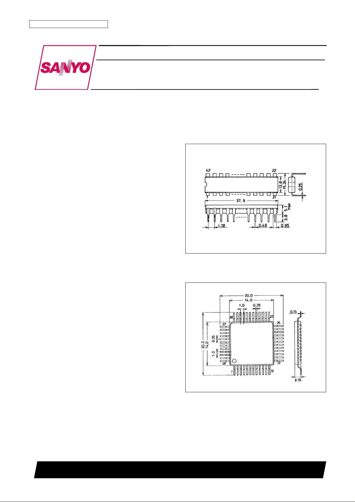
Package Dimensions
unit: mm
3025B-DIP42S
unit: mm
3052A-QFP48A
Preliminary
SANYO: DIP42S
[LC89080]
SANYO: QFP48A
[LC89080Q]
LC89080, 89080Q
SANYO Electric Co.,Ltd. Semiconductor Bussiness Headquarters
TOKYO OFFICE Tokyo Bldg., 1-10, 1 Chome, Ueno, Taito-ku, TOKYO, 110-8534 JAPAN
Video Signal 3-Channel 8-Bit D/A Converter
CMOS LSI
Specifications
Absolute Maximum Ratings at Ta = 25°C, VSS= 0 V
Allowable Operating Ranges
Electrical Characteristics at Ta = 25°C, VDD= 5.0 V, V
REF
IN = 1.0 V, R
REF
= 300 Ω, RO= 75 Ω
No. 4030-2/8
LC89080, 89080Q
Parameter Symbol Conditions Ratings Unit
Maximum supply voltage V
DD
max –0.3 to +7.0 V
Input voltage V
IN
–0.3 to VDD+ 0.3 V
Operating temperature Topr –30 to +75 °C
Storage temperature Tstg –40 to +125 °C
Parameter Symbol Conditions min typ max Unit
Supply voltage V
DD
4.5 5.0 5.5 V
Reference voltage input V
REF
IN 1.0 2.0 V
Output resistance R
O
75 Ω
Input high-level voltage V
IH
2.2 VDD+ 0.3 V
Input low-level voltage V
IL
–0.3 +0.8 V
Phase compensation capacitance Ccomp 1 µF
Parameter Symbol Conditions min typ max Unit
Resolution RES 8 Bits
Maximum conversion speed Fs max 30 MSPS
Power dissipation Pd Fs = 30 MSPS 330 400 mW
Zero-scale output voltage Vzero For each channel –15 0 +15 mV
Full-scale output voltage Vfull For each channel 0.92 1.00 1.08 V
Full-scale voltage ratio FSR 0 4 8 %
Linearity error I.L. DC precision ±1.0 LSB
Differential linearity error D.L. DC precision ±0.5 LSB
Reference voltage output V
REF
OUT 0.99 1.00 1.01 V
Pin Assignment LC89080 (DIP42S)
No. 4030-3/8
LC89080, 89080Q
Pin No. Symbol Description
1 DV
DD
Digital system power supply (+5 V)
2 DA1 Channel A digital input (MSB)
3 to 8 DA2 to DA7 Channel A digital input
9 DA8 Channel A digital input (LSB)
10 DB1 Channel B digital input (MSB)
11 to 16 DB2 to DB7 Channel B digital input
17 DB8 Channel B digital input (LSB)
18 DC1 Channel C digital input (MSB)
19 to 24 DC2 to DC7 Channel C digital input
25 DC8 Channel C digital input (LSB)
26 CLK Clock input
27 DV
DD
Digital system power supply (+5 V)
28 DGND Digital system ground (0 V)
29 ICOB Channel C negative output. Connect to A.GND through an output resistor R
O
(usually 75 Ω).
30 ICO Channel C positive output. Connect to A.GND through an output resistor R
O
(usually 75 Ω).
31 AV
DD
Analog system power supply (+5 V)
32 IBOB Channel B negative output. Connect to A.GND through an output resistor R
O
(usually 75 Ω).
33 IBO Channel B positive output. Connect to A.GND through an output resistor R
O
(usually 75 Ω).
34 AGND Analog system ground (0 V)
35 IAOB Channel A negative output. Connect to A.GND through an output resistor R
O
(usually 75 Ω).
36 IAO Channel A positive output. Connect to A.GND through an output resistor R
O
(usually 75 Ω).
37 AV
DD
Analog system power supply (+5 V)
38 COMP Phase compensation capacitor. Connect a 1 µF capacitor between this pin and ground.
39 I
REF
Reference current output. Connect a resistor that is 4 times the output resistance ROto this pin.
40 V
REF
IN Reference voltage input. This input pin sets the analog output dynamic range.
41 V
REF
OUT
Reference voltage output. The output voltage is set to 0.2 times V
DD
by a resistor divider.
When V
DD
is 5.0 V, a 1.0 V reference voltage can be acquired from pin 40.
42 DGND Digital system ground (0 V)

Pin Assignment LC89080Q (QFP48A)
No. 4030-4/8
LC89080, 89080Q
Pin No. Symbol Description
1 to 3 DA5 to 7 Channel A digital input
4 DA8 Channel A digital input (LSB)
5 DB1 Channel B digital input (MSB)
6 NC Unused (no connection)
7 to 12 DB2 to DB7 Channel B digital input
13 DB8 Channel B digital input (LSB)
14 DC1 Channel C digital input (MSB)
15 to 18 DC2 to DC5 Channel C digital input
19 DV
DD
Digital system power supply (+5 V)
20 DC6 Channel C digital input
21 DC7 Channel C digital input
22 DC8 Channel C digital input (LSB)
23 CLK Clock input
24 NC Unused (no connection)
25 DV
DD
Digital system power supply (+5 V)
26 DGND Digital system ground (0 V)
27 ICOB Channel C negative output. Connect to A.GND through an output resistor R
O
(usually 75 Ω).
28 ICO Channel C positive output. Connect to A.GND through an output resistor R
O
(usually 75 Ω).
29 AV
DD
Analog system power supply (+5 V)
30 AV
DD
Analog system power supply (+5 V)
31 IBOB Channel B negative output. Connect to A.GND through an output resistor R
O
(usually 75 Ω).
32 IBO Channel B positive output. Connect to A.GND through an output resistor R
O
(usually 75 Ω).
33 AGND Analog system ground (0 V)
34 IAOB Channel A negative output. Connect to A.GND through an output resistor R
O
(usually 75 Ω).
35 IAO Channel A positive output. Connect to A.GND through an output resistor R
O
(usually 75 Ω).
36 AV
DD
Analog system power supply (+5 V)
37 COMP Phase compensation capacitor. Connect a 1 µF capacitor between this pin and ground.
38 NC Unused (no connection)
39 I
REF
Reference current output. Connect a resistor that is 4 times the output resistance ROto this pin.
40 V
REF
IN Reference voltage input. This input pin sets the analog output dynamic range.
41 V
REF
OUT
Reference voltage output. The output voltage is set to 0.2 times V
DD
by a resistor divider.
When V
DD
is 5.0 V, a 1.0 V reference voltage can be acquired from pin 40.
42 DGND Digital system ground (0 V)
43 DV
DD
Digital system power supply (+5 V)
44 DV
DD
Digital system power supply (+5 V)
45 DA1 Channel A digital input (MSB)
46 to 48 DA2 to DA4 Channel A digital input

LC89080 Operation
The LC89080 and LC89080Q include three current-matrix D/A converters on chip. These D/A converters each have 63
basic current cells (with current weight I) and two weighted current cells (I/2 and I/4). These current cells are turned on
or off according to the input digital code (a binary code). The sum of these currents is output to the output pins (IO and
IOB) and the output current is converted to a voltage by the output resistor (RO) to acquire the analog output. The table
shows the ideal relationship between the digital input and the analog output when V
REF
IN is 1 V.
Sample Application Circuit: LC89080
No. 4030-5/8
LC89080, 89080Q
Digital input code Analog output voltage
D1
D2 D3 D4 D5 D6 D7
D8 IO IOB
MSB LSB (positive output) (negative output)
0 0 0 0 0 0 0 0 0 0.996
0 0 0 0 0 0 0 1 0.004 0.992
0 0 0 0 0 0 1 0 0.008 0.988
0 1 1 1 1 1 1 1 0.496 0.500
1 0 0 0 0 0 0 0 0.500 0.496
1 1 1 1 1 1 0 1 0.988 0.008
1 1 1 1 1 1 1 0 0.992 0.004
1 1 1 1 1 1 1 1 0.996 0

Sample Application Circuit: LC89080Q
Application circuit in which the output resistance is 75 Ω and the internally generated 1-V reference voltage is used.
AC Characteristics at Ta = –30 to 70°C, VDD= 4.5 to 5.5 V
No. 4030-6/8
LC89080, 89080Q
Parameter Symbol Conditions min typ max Unit
Data setup time ts 15 ns
Data hold time th 15 ns
Output delay time td 10 ns

Timing Chart
The digital inputs for all 3 channels are acquired on the rising edge of the clock input, after which the corresponding
analog voltages are output.
No. 4030-7/8
LC89080, 89080Q

No. 4030-8/8
LC89080, 89080Q
Block Diagram
This catalog provides information as of February, 1997. Specifications and information herein are subject to
change without notice.
■ No products described or contained herein are intended for use in surgical implants, life-support systems, aerospace
equipment, nuclear power control systems, vehicles, disaster/crime-prevention equipment and the like, the failure of
which may directly or indirectly cause injury, death or property loss.
■ Anyone purchasing any products described or contained herein for an above-mentioned use shall:
➀ Accept full responsibility and indemnify and defend SANYO ELECTRIC CO., LTD., its affiliates, subsidiaries and
distributors and all their officers and employees, jointly and severally, against any and all claims and litigation and all
damages, cost and expenses associated with such use:
➁ Not impose any responsibility for any fault or negligence which may be cited in any such claim or litigation on
SANYO ELECTRIC CO., LTD., its affiliates, subsidiaries and distributors or any of their officers and employees
jointly or severally.
■ Information (including circuit diagrams and circuit parameters) herein is for example only; it is not guaranteed for
volume production. SANYO believes information herein is accurate and reliable, but no guarantees are made or implied
regarding its use or any infringements of intellectual property rights or other rights of third parties.
 Loading...