

Page 1
Ordering number : ENN*6689
CMOS IC
LC86P6449
8-Bit Single Chip Microcontroller
with One-Time Programmable PROM
Preliminary
Overview
The LC86P6449 is a CMOS 8-bit single chip microcontroller with one-time PROM for the LC866400 series.
This microcontroller has the function and the pin description of the LC866400 series mask ROM version, and 48K-byte
PROM.
Features
(1) Option switching by PROM data
The option function of the LC866400 series can be specified by the PROM data.
LC86P6449 can be checked the function of the trial pieces using the mass production board.
(2) Internal one-time PROM capacity : 49408 bytes
(3) Internal RAM capacity : 1152 bytes
Used PROM or RAM capacity are equal ROM or RAM capacity of mask ROM version which applies LC86P6449.
Mask ROM version PROM capacity RAM capacity
LC866448 49152 bytes 1152 bytes
LC866444 45056 bytes 1152 bytes
LC866440 40960 bytes 1152 bytes
LC866436 36864 bytes 1152 bytes
LC866432 32768 bytes 768 bytes
LC866428 28672 bytes 768 bytes
LC866424 24576 bytes 768 bytes
LC866420 20480 bytes 640 bytes
LC866416 16384 bytes 640 bytes
LC866412 12288 bytes 512 bytes
LC866408 8192 bytes 512 bytes
Programming service
We offers various services at nominal charges. These include the ROM writing, the ROM reading, the package stamping
and the screening. Contact our representative for further information
Ver.1.01
80796
91400 RM (IM) SK No.6689-1/22
Page 2
LC86P6449
(4) Operating supply voltage : 4.5V to 6.0V
(5) Instruction cycle time : 1.0µs to 366µs
(6) Operating temperature : -30°C to +70°C
(7) The pin and the package compatible with the LC866400 series mask ROM devices
(8) Applicable mask ROM version : LC866448/LC866444/LC866440/LC866436//LC866 432/LC866428
/LC866424/LC866420/LC866416/LC866412/LC866408
Notice for use
LC86P6449 is provided for the first release and small shipping of the LC866400 series.
At using, take notice of the followings.
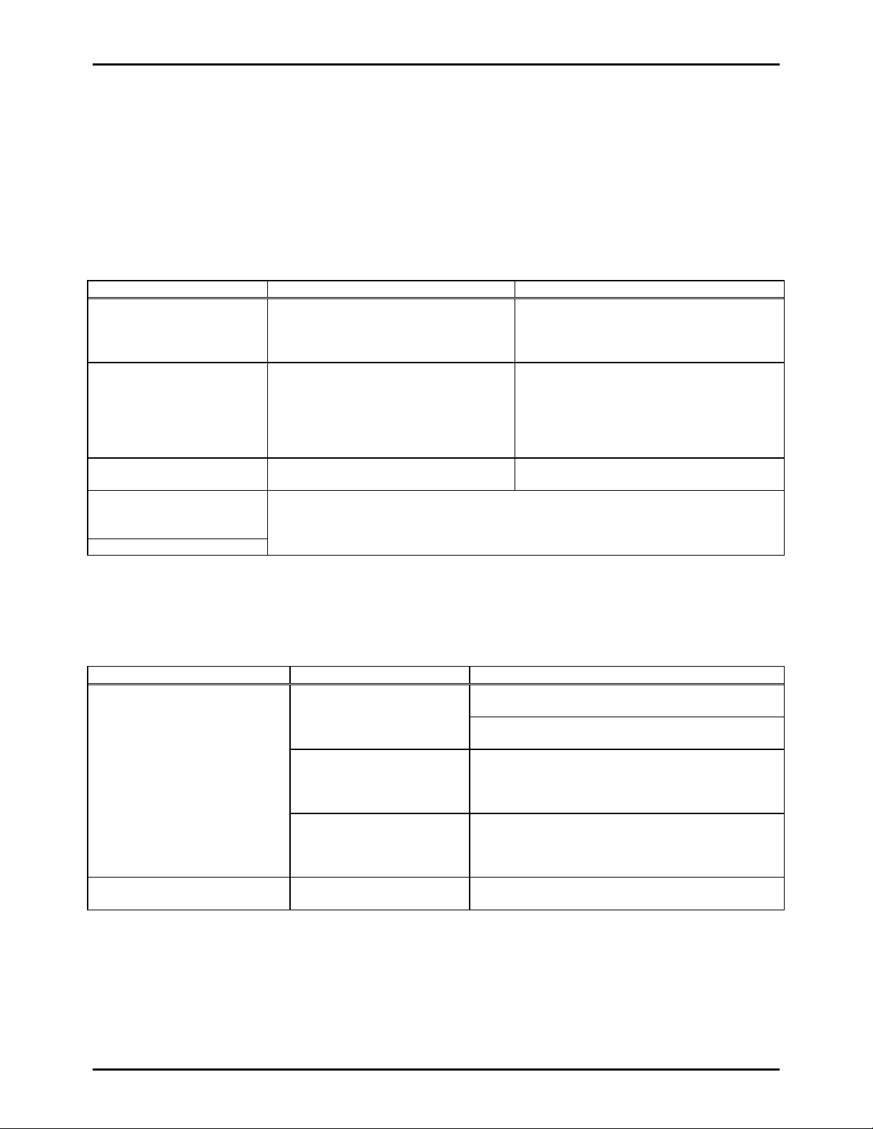
(1) A point of difference LC86P6449 and LC866400 series
Item LC86P6449 LC866448/44/40/36/32/28/24/20/16/12/08
Operation after reset
releasing
Pull-down resistor of
the following pins
•S0/T0 – S6/T6
•S7/T7 – S15/T15
•S16 – S27
•S28 – S37
Operating supply
Voltage range (VDD)
“L” level hold Tr. of the
high voltage withstand input
terminal
Power dissipation
LC86P6449 uses 256 bytes that is addressed on FF00H to FFFFH in the program memory as the option configuration
data area. This option configuration cannot execute all options which LC866400 series have. Next tables show the
options that correspond and not correspond to LC86P6449.
• A kind of the option corresponding of the LC86P6449
A kind of option Pins, Circuits Contents of the option
Input/output form of
Input/output ports
Pull-up MOS Tr. of input ports Port 7
*1) Specified in a bit
*2) Specified in nibble unit. T he port of N-channel open drain output does not have the Pull-up MOS Tr..
The option is specified until 3ms after
going to a ‘H’ level to the reset terminal by
dgrees. The program is executed from
00H of the program counter.
Pull-down resistor
provided/not provided
Not provi ded
Provided (fixed)
Provided (fixed)
Not provi ded
4.5V to 6.0V 2.5V to 6.0V
Refer to ‘electrical characteristics’ on the semiconductor news.
Port 0
Port 1
*1
Port 3
*1
*1
1. N-channel open drain output
2. CMOS output *1
1. Pull-up MOS Tr. proveded
2. Pull-up MOS Tr. not provided *2
1. Input : Programmable pull-up MOS Tr.
2. Input : Programmable pull-up MOS Tr.
1. Input : No Programmable pull-up MOS Tr.
2. Input : Programmable pull-up MOS Tr.
1. No Pull-up MOS Tr.
2. Pull-up MOS Tr.
The program is executed from 00H of the
program counter immediately after going to a
‘H’ level to reset terminal.
Pull-down resistor
provided/not provided
Specified by the option
Provided (fixed)
Specified by the option
Specified by the option
Output : N-channel open drain
Output : CMOS
Output : N-channel open drain
Output : CMOS
No.6689-2/22
Page 3
LC86P6449
• A kind of the option not corresponding of the LC86P6449
A kind of option Pins, Circuits LC86P6449 LC866448/44/40/36/32/28/24/2 0/16/12/08
Pull-down resistor of
the high voltage
Withstand output terminals
•S0/T0 to S6/T6
•S16 to S27
•S28 to S37
Not provi ded
Provided (fixed)
Not provi ded
Specified by the option
Specified by the option
Specified by the option
(2) Option
The option data is created by the option specified program “SU86K.EXE”. The created option data is linked to the
program area by linkage loader “L86K.EXE” .
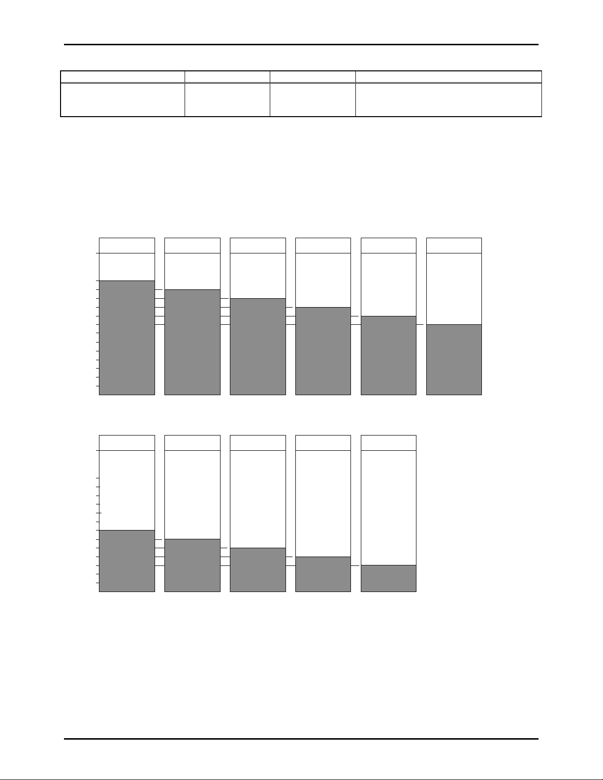
(3) ROM space
LC86P6449 and LC86 64 00 seri es use 25 6 bytes that is ad dres sed on 0 FF0 0H t o 0F FFFH in the p ro gr am memory as the
option specified data area. These program memory capacity are 61440 bytes that is addressed on 0000H to BFFFH.
0FFFFH
0FF00H
0EFFFH
0DFFFH
0CFFFH
0BFFFH
0AFFFH
9FFFH
8FFFH
7FFFH
6FFFH
5FFFH
4FFFH
3FFFH
2FFFH
1FFFH
0FFFH
0000H
The option specified
area 256 bytes
Program area
48K bytes
LC866448
The option
specified area
Program area
44K bytes
LC866444
The option
specified area
Program area
40K bytes
LC866440
The option
specified area
Program area
36K bytes
LC866436
The option
specified area
Program area
32K bytes
LC866432
The option
specified area
Program area
28K bytes
LC866428
0FFFFH
0FF00H
0EFFFH
0DFFFH
0CFFFH
0BFFFH
0AFFFH
9FFFH
8FFFH
7FFFH
6FFFH
5FFFH
4FFFH
3FFFH
2FFFH
1FFFH
0FFFH
0000H
The option
specified area
Program area
24K bytes
LC866424
The option
specified area
Program area
20K bytes
LC866420
The option
specified area
Program area
16K bytes
LC866416
The option
specified area
Program area
12K bytes
LC866412
The option
specified area
Program area
8K bytes
LC866408
No.6689-3/22
Page 4
LC86P6449
(4) Ordering information
1. When ordering the identical mask ROM and PROM devices simultaneously.
Provide an EPROM containing the target memory contents together with the separate order forms for each of the mask
ROM and PROM versions.
2. When ordering a PROM device.
Provide an EPROM containing the target memory contents together with an order form.
How to use
(1) Specification of option
Programming data for PROM of the LC86P6449 is required.
Debugged evaluation file (EVA file) must be converted to an INTEL-HEX formatted file (HEX file) with file converter
program, EVA2HEX.EXE. The HEX file is used as the programming data for the LC86P6449.
(2) How to program for the PROM
LC86P6449 can be programmed by the EPROM programmer with attachment ; W86EP6448Q.
• Recommended EPROM programmer
Productor EPROM programmer
Advantest R4945, R4944, R4943
Andou AF-9704
AVAL PKW-1100, PKW-3000
Minato electronics MODEL 1890A
• “27512 (Vpp=12.5V) Intel high speed programming” mode available. The address must be set to “0 to
0FFFFH” and a jumper (DASEC) must be set to ‘OFF’ at programming
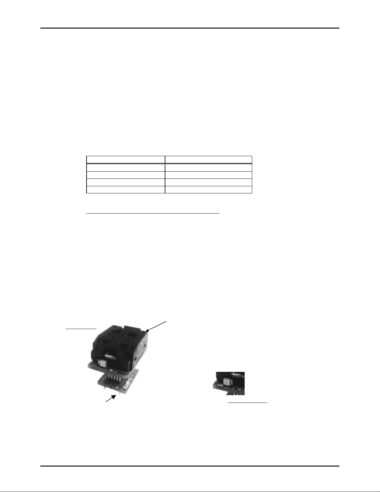
(3) How to use th e data secur ity function
“Data security” is the disabled function to read the data of the PROM.
The following is the process in order to execute the data security.
1. Set ‘ON’ the jumper of attachment.
2.Program again. Then EPROM programmer displays the error. The error means normally activity of the data
security. It is not a trouble of the EPROM programmer or the LSI.
Notes
• Data security is not executed when the data of all address have ‘FFH’ at the sequence 2 above.
• The programming by a sequential operation “BLANK⇒PROGRAM⇒VERIFY” cannot be executed data security at the
sequence 2 above.
• Set to ‘OFF’ the jumper after executing the data security.
Data security
1 pin mark
of LSI
.
1 pin
Not data security
W86EP6448Q
No.6689-4/22
Page 5
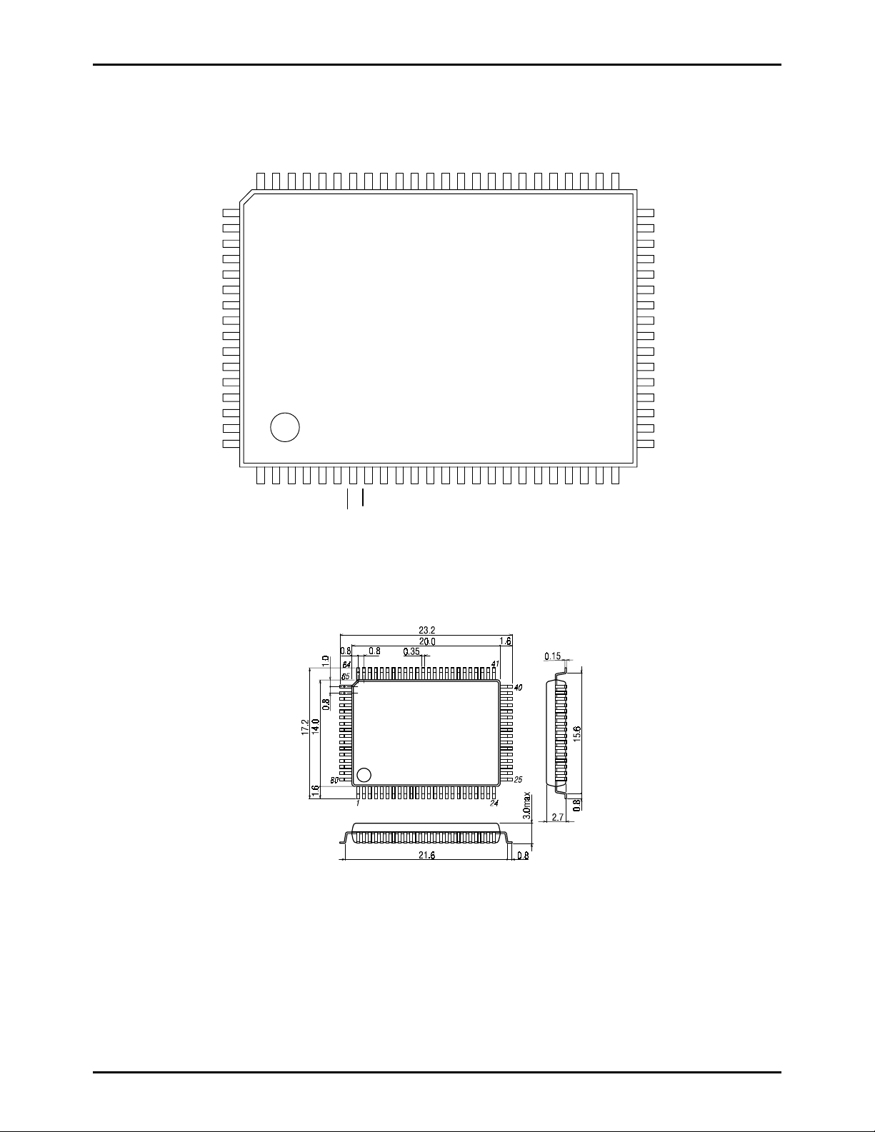
Pin Assignment
N
N
P00
P01
P02
P03
P04
P05
P06
P07
VSS2
P10/SO0
P11/SI0/SB0
P12/SCK0
P13/SO1
P14/SI1/SB1
P15/SCK1
P16/BUZ
Package Dimension
(unit : mm)
3174
LC86P6449
S37/PE5
S36/PE4
S35/PE3
S34/PE2
S33/PE1
S32/PE0
S31/PD7
S30/PD6
S29/PD5
S28/PD4
S27/PD3
S26/PD2
S25/PD1
S24/PD0
S23/PC7
S22/PC6
S21/PC5
S20/PC4
S19/PC3
S18/PC2
6463626160595857565554535251504948474645444342
65
66
67
68
69
70
71
72
73
74
75
76
77
78
79
80
1 2 3 4 5 6 7 8 9
P30
P31
P32
P33
RES
P17/PWM0
P70/INT0
10
11
12
13
14
15
16
17
18
19
20
P74
XT1/
CF1
CF2
VSS1
XT2/P75
VDD1
P80/AN0
P81/AN1
P82/AN2
P83/AN3
P84/AN4
P85/AN5
P86/AN6
S17/PC1
21
P87/AN7
S16/PC0
22
P71/INT1
VP
23
P72/INT2/T0I
VDD2
41
40
39
38
37
36
35
34
33
32
31
30
29
28
27
26
25
24
P73/INT3/T0I
S15/T15
S14/T14
S13/T13
S12/T12
S11/T11
S10/T10
S9/T9
S8/T8
S7/T7
S6/T6
S5/T5
S4/T4
S3/T3
S2/T2
S1/T1
S0/T0
SANYO : QIP-80E
No.6689-5/22
Page 6
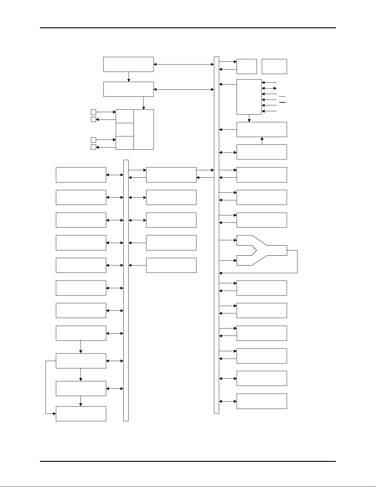
System Bl ock Diagram
Interrupt Control
Stand-by C ontr ol
Base Timer
SIO0
SIO1
Timer 0
Timer 1
ADC
INT0 to 3
Noise Filter
Real Time Service
RAM
128 bytes
VFD
Controller
High Voltage Output
CF
RC
X’tal
Clock
Generator
LC86P6449
Bus Interface
Port 1
Port 3
Port 7
Port 8
IR PLA
PROM
Control
PROM(48KB)
PC
ACC
B Register
C Register
ALU
PSW
RAR
RAM
Stack Pointer
Port 0
Watchdog T ime r
A15-A0
D7-D0
TA
CE
OE
DASEC
No.6689-6/22
Page 7
LC86P6449
e
d
d
e
d
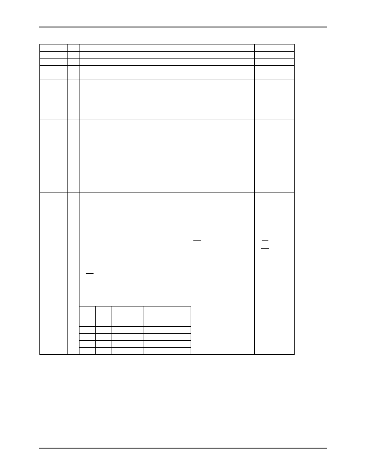
LC86P6449 Pin description
Pin name I/O Function description Option PROM mode
VSS1,2 - Power pin (-) - VDD1,2 - Power pin (+) *4 Refer to Notes - VP - P ower pin (-) for the VFD output pull-down
resist
PORT0
P00 to P07
I/O •8-bit input/output port
•Input for port 0 inter rupt
•Input/output in nibble units
•Input for HOL D rel ease
•15V withstand at N- channel open drain
output
PORT1
P10 to P17
I/O •8-bit input/output port
•Input/output can be specified in a bit unit
•Other pin functions
P10 SIO0 data output
P1 1 SIO 0 data input/bus input/output
P1 2 SIO0 clock input/output
P13 SIO1 data output
P1 4 SIO 1 data input/bus input/output
P15 SIO1 clock input/output
P16 Buzzer output
P1 7 Timer 1 output (PWM0 output)
PORT3
P30 to P33
I/O •4-bit input/output port
•Input/output can be specified
•15V withstand at N- channel open drain
output
PORT7
P70
P71 to P75
•6-bit input port
•Other functio n s
P70 : INT0 input/HOLD release input/
I/O
I
N-ch Tr. output for watchdog timer
P71 : INT1 input/HOLD release input
P72 : INT2 input/timer 0 event input
P73 : INT3 input with noise rejection
filter/timer 0 event input
P74
: XT1 terminal for 32.768kHz crystal
oscillation
P7 5 : XT 2 terminal for 32.768kHz crystal
oscillation
•Interrupt received forms, the vector addresses
rising falling rising
&
high
level
low
level
falling
INT0 enable enable disableenable enable 03H
INT1 enable enable disableenable enable 0BH
INT2 enable enable enable disabl
INT3 enable enable enable
isabl
isable13H
isable1BH
Continue.
- -
•Pull-up resistor :
-
Provided/Not provided
•Output form :
CMOS/N-channel open
drain
•Output form :
CMOS/N-channel open
Data line
D0 to D7
drain
•Output form :
CMOS/N-channel open
drain
Pull-up resistor :
Provided/Not provided
(P70,71,72,73)
P74
,P75 don’t have
*
pull-up
PROM control
signals
DASEC (*1)
OE
(*2)
‚bE
(*3)
CE
resistor option.
vector
No.6689-7/22
Page 8

LC86P6449
Pin name I/O Function description Option PROM mode
PORT8
P80 to 87
I •8-bit input port
•Other functio n
- -
AD input port (8 port pins)
S0/T0 to
S6/T6 *6
S7/T7 to
S15/T15
*7
S16 to S31
*8
O Output for VFD displa y controll er
Segment/tim i ng in common
O •Output for VFD display cont roller
Segment/timing with interna l pull-down
resistor in common
I/O •Output for VFD display controller Segment
output
•Other functio n
S16 : High voltage input port PC0
S17 : High voltage input port PC1
- -
- TA (*5)
- •Address input
A15 to A0
•PROM
control
signal input
S18 : High voltage input port PC2
S19 : High voltage input port PC3
S20 : High voltage input port PC4
S21 : High voltage input port PC5
S22 : High voltage input port PC6
S23 : High voltage input port PC7
S24 : High voltage input port PD0
S25 : High voltage input port PD1
S26 : High voltage input port PD2
S27 : High voltage input port PD3
S28 : High voltage input port PD4
S29 : High voltage input port PD5
S30 : High voltage input port PD6
S31 : High voltage input port PD7
S32 to S37
*9
I/O •Output for VFD display controller Segment
•Other functio n
- -
S32 : High voltage I/O port PE0
S33 : High voltage I/O port PE1
S34 : High voltage I/O port PE2
S35 : High voltage I/O port PE3
S36 : High voltage I/O port PE4
S37 : High voltage I/O port PE5
RES
XT1/
I Reset pin - I •Input pin for 32.768kHz crystal oscillation
P74
- -
•Other functio n
P74
XT 1 : Input port
In case of non use, connect to VDD1.
XT2/P75 O •Output pin for 32.768kHz crystal
- -
oscillation
•Other functio n
XT 2 : Input port P75
In case of non use, connect to VDD1 at using
as port or unconnect at using as oscillation.
No.6689-8/22
Page 9
LC86P6449
Pin name I/O Function description Option PROM mode
CF1 I Input pin for the ceramic resonator oscillat ion - CF2 O Output pin for the ceramic resonator oscillation - -
♦ All of port options except the pull-up resistor option of port 0 can be specified in a bit unit.
*1 Memory select input for data security
*2 Output enable input
*3 Chip enable input
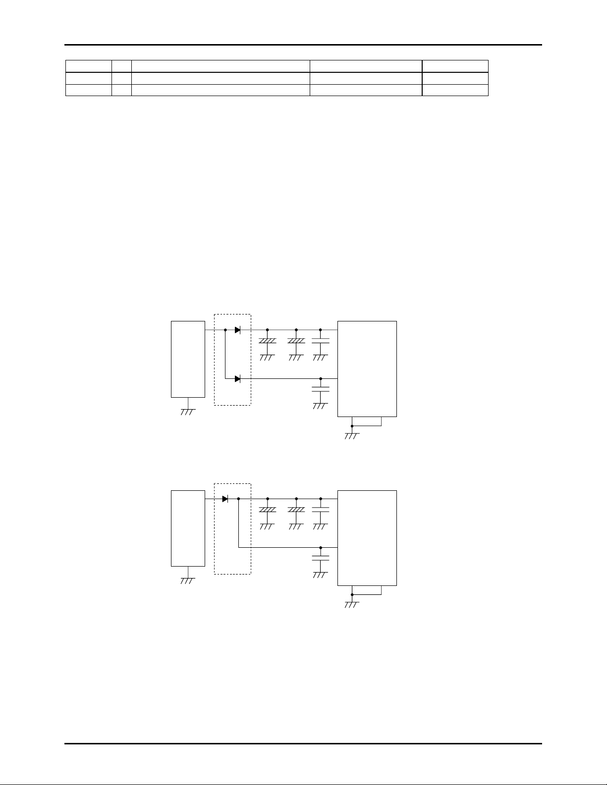
*4 Connect like the following figure to reduce noise into a VDD1 terminal.
*5 TA ! PROM control signal input
*6 S0/T0 to S6/T6 : not provided the pull-down resistor
*7 S7/T7 to S15/T15 : provided the pull-down resistor (fixed)
*8 S16 to S27 : provided the pull-down resistor (fixed)
*9 S28 to S31 : not provided the pull-down resistor
*10 S32 to S37 : not provided the pull-down resistor
[Notes]
When connecting to the power supply, the power pins must be connected like following figure.
For the LC866448B/44B/40B/36B
Power
Supply
For back-up
LSI
VDD1
VDD2
(VFD power pin)
VSS1 VSS2
For the LC866432A/28A/24A/20A/16A/12A/08A
Power
Supply
For back-up
LSI
VDD1
VDD2
(VFD power pin)
VSS1 VSS2
No.6689-9/22
Page 10

LC86P6449
V
1. Absolute Maximu m Ratings at VSS1=VSS2=0V and Ta=25°C
Parameter Symbol Pins Conditions
Supply voltage VDDMAX VDD1, VDD2 VDD1=VDD2 -0.3 +7.0
Input voltage
VI(1)
•Ports 71,72,73,
RES
•
74
,75,8
-0.3 VDD+0.3
Ratings
DD[V] min. typ. max.
unit
V
VI(2) VP VDD-45 VDD+0.3
Output voltage VO(1) S0/T0 to S15/T15 VDD-45 VDD+0.3
Input/Output
voltage
VIO(1) •Port 1
•Port 70
-0.3 VDD+0.3
•Ports 0, 3 of CMOS
output
VIO(2) Ports 0, 3 of open
-0.3 15
drain output
VIO(3) S16 to S37 VDD-45 VDD+0.3
High
level
output
current
Low
level
output
current
Peak
output
current
Total
output
current
output
current
Total
output
IOPH(1) Ports 0, 1, 3 •CMOS output
•At each pins
IOPH(2) S0/T0 to S15/T1 5 At each pi ns -30
IOPH(3) S16 to S37 At each pins -15
ΣIOAH(1)
IOAH(2)
Σ
ΣIOAH(3)
Ports 0,1,3 The total of all pins -30
S0/T0 to S15/T15 The total of all pins -55
S16 to S37 The total of all pins -115
IOPL(1) Ports 0,1,3 At each pins 20 Peak
IOPL(2) Port 70 At each pins 15
IOAL(1)
Σ
ΣIOAL(2)
Port 0 The total of all pins 40
Ports 1,3 The total of all pins 40
-10
mA
current
Maximum power
dissipation
Operating
Pdmax QFP80E
Ta=-30 to+70°C
480
Topr -30 70
mW
C
°
temperature
range
Storage
Tstg -55 125
temperature
range
No.6689-10/22
Page 11
LC86P6449
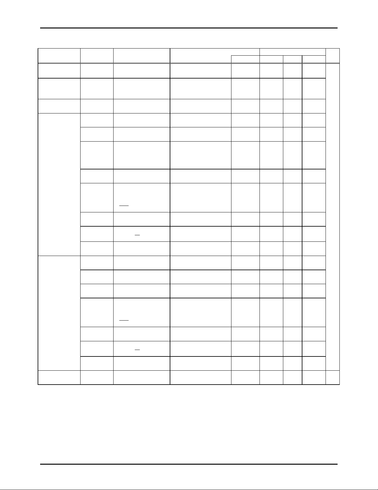
2. Recommended Operating Range at Ta=-30°C to +70°C, VSS1=VSS2=0V
Parameter Symbol Pins Conditions
Operating
Supply voltage
VDD(1) VDD1=VDD2
98µs≤tCYC
tCYC≤400µs
Hold voltage VHD VDD1=VDD2 RAMs and t he re gist e r s
hold voltage at HOLD
mode.
Pull-down
VP VP 4.5 to 6.0 -35 VDD
Voltage
Input high
voltage
VIH(1) Port 0 at CMOS
output
VIH(2) Port 0 at open drain
Output disable 4.5 to 6.0 0.33VDD
Output disable 4.5 to 6.0 0.75VDD 13.5
output
VIH(3) •Port 1
Output disable 4.5 to 6.0 0.75VDD VDD
•Ports 72,73
•Port 3 at CMOS
output
VIH(4) •Port 3 at open
Output disable 4.5 to 6.0 0.75VDD 13.5
drain output
VIH(5) •Port 70
Port input/interrupt
Output N-channel
Tr. OFF
•Port 71
RES
•
VIH(6) Port 70
Watchdog timer
VIH(7) •Port 8
74
•Ports
,75
Output N-channel
Tr. OFF
Using as port 4.5 to 6.0 0.75VDD VDD
VIH(8) S16 to S3 7 Output P-channel
Tr. OFF
Input low
voltage
VIL(1) Port 0 at CMOS
output option
VIL(2) Port 0 at open
Output disable 4.5 to 6.0 VSS 0.2VDD
Output disable 4.5 to 6.0 VSS 0.25VDD
drain output
VIL(3) •Ports 1,3
Output disable 4.5 to 6.0 VSS 0.25VDD
•Ports 72,73
VIL(4) •Port 70
Port input/interrupt
Output N-channel
Tr. OFF
•Port 71
RES
•
VIL(5) Port 70
Watchdog timer
VIL(6) •Port 8
•Ports
74
,75
Output N-channel
Tr. OFF
Using as port 4.5 to 6.0 VSS 0.25VDD
VIL(7) S16 to S37 Output P-channel
Tr. OFF
Operation
tCYC 4.5 to 6.0 0.98 400
cycle time
Continue.
Ratings
VDD[V] min. typ. max.
4.5 6.0
2.0 6.0
VDD
+1.0
4.5 to 6.0 0.75VDD VDD
4.5 to 6.0 0.9VDD VDD
4.5 to 6.0
0.
33VDD
VDD
+1.0
4.5 to 6.0 VSS 0.25VDD
4.5 to 6.0 VSS
8VDD
0.
-1.0
4.5 to 6.0 VP 0.2VDD
unit
V
µs
No.6689-11/22
Page 12
LC86P6449
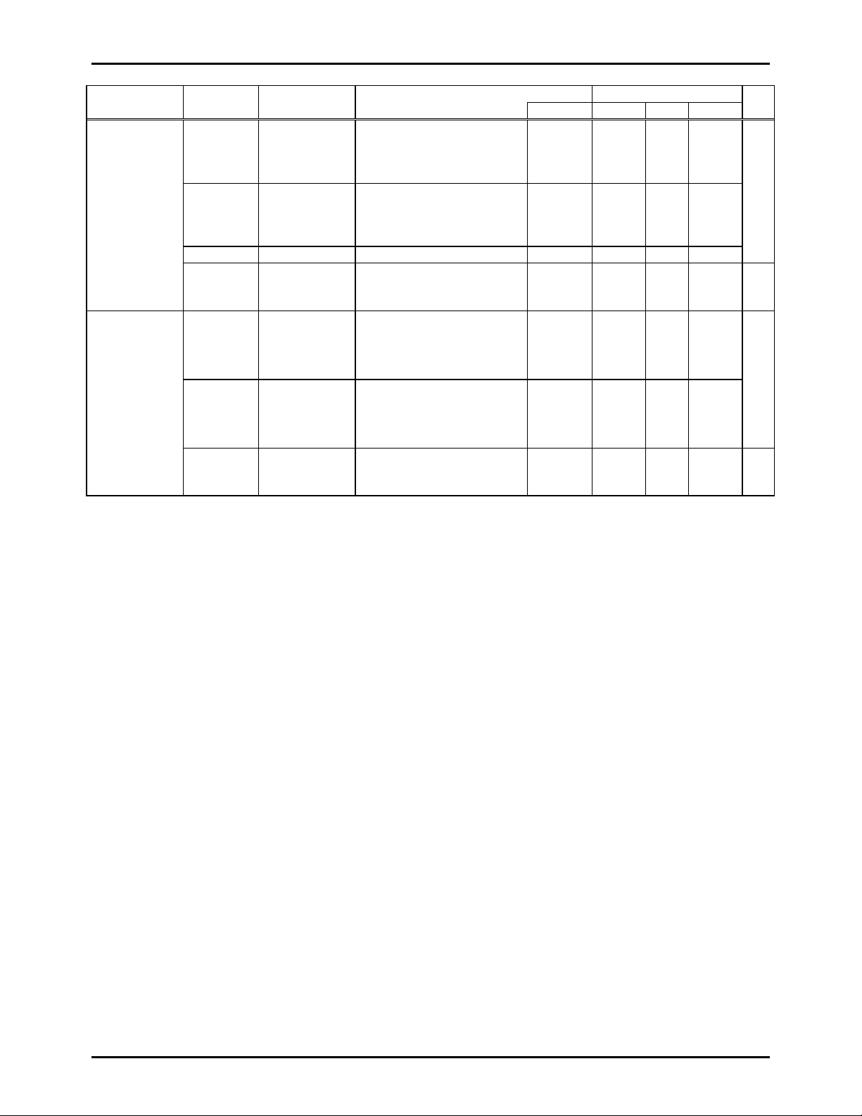
Parameter Symbol Pins Conditions
Oscillation
frequency
range
(Note 1)
FmCF(1) CF1, CF2 •6MHz
(ceramic resonator
oscillation)
•Refer to figure 1
FmCF(2) CF1, CF2 •3MHz
(ceramic resonator
oscillation)
•Refer to figure 1
FmRC RC oscillation 4.5 to 6.0 0.3 0.8 3.0
FsXtal XT1, XT2 •32.768kHz
(crystal oscillation)
•Refer to figure 2
Oscillation
stabilizing
time period
(Note 1)
tmsCF(1) CF1, CF2 •6MHz
(ceramic resonator
oscillation)
•Refer to figure 3
tmsCF(2) CF1, CF2 •3MHz
(ceramic resonator
oscillation)
•Refer to figure 3
tssXtal XT1, XT2 •32.768kHz
(crystal oscillation)
•Refer to figure 3
(Note 1) The oscillation constant is shown on table 1 and table 2.
Ratings
VDD[V] min. typ. max.
4.5 to 6.0 6
unit
MHz
4.5 to 6.0 3
4.5 to 6.0 32.768 kHz
4.5 to 6.0
ms
4.5 to 6.0
4.5 to 6.0 s
No.6689-12/22
Page 13
LC86P6449
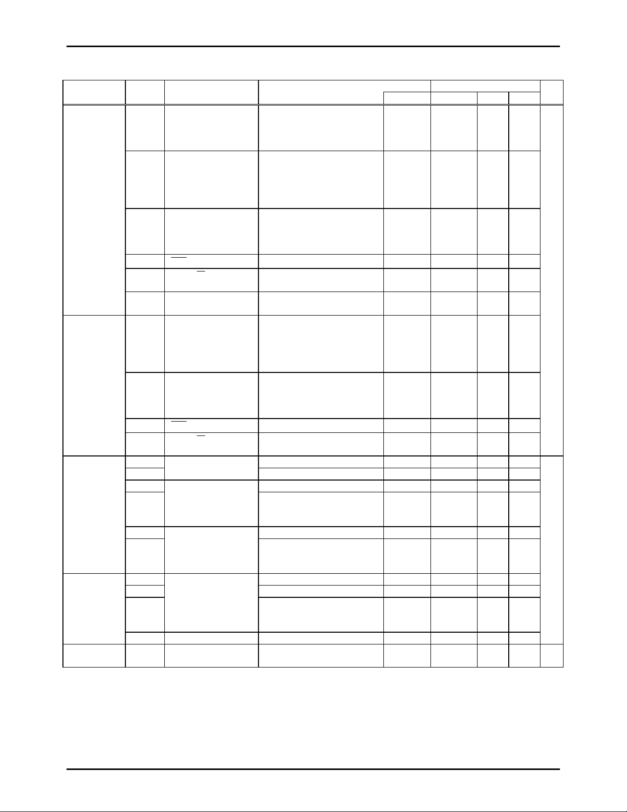
3. Electrical Characteristics at Ta=-30°C to +70°C, VSS1=VSS2=0V
Parameter Symbol Pins Conditions
Input high
current
IIH(1) Ports 0,3 at open
drain output
•Output disable
•VIN=13.5V
(including off-leakage
current of output Tr.)
IIH(2) •Ports 1,3
•Port 0 without
pull-up MOS Tr.
•Output disable
•Pull-up MOS Tr. OFF.
•VIN=VDD
(including off-leakage
current of output Tr.)
IIH(3) •Ports 70,71,72,73
VIN=VDD 4.5 to 6.0 1
without pull-up
MOS Tr.
•Por t 8
IIH(4)
IIH(5)
RES
Ports
74
,75
VIN=VDD 4.5 to 6.0 1
Using as port
VIN=VDD
IIH(6) •S28 to S37 •Output disable
•VIN=VDD
Input low
current
IIL(1) •Ports 1,3
•Port 0 without
pull-up MOS Tr.
•Output disable
•Pull-up MOS Tr. OFF.
•VIN=VSS
(including off-leakage
current of output Tr.)
IIL(2) •Ports 70,71,72,73
VIN=VSS 4.5 to 6.0 -1
without pull-up
MOS Tr.
•Por t 8
IIL(3)
IIL(4)
RES
Ports
74
,75
VIN=VSS 4.5 to 6.0 -1
Using as port
VIN=VSS
Output high
voltage
VOH(1) IOH=-1.0mA 4.5 to 6.0 VDD-1
VOH(2)
VOH(3) IOH=-20mA 4.5 to 6.0 VDD-1.8
VOH(4)
Ports 0,1,3 of
CMOS output
S0/T0 to S15 / T15
IOH=-0.1mA 4.5 to 6.0 VDD-0.5
•IOH=-1.0mA
•The current of these each
pins is not over 1mA.
VOH(5) IOH=-5mA 4.5 to 6.0 VDD-1.8
VOH(6)
S16 to S37
•IOH=-1.0mA
•The current of these each
pins is not over 1mA.
Output low
voltage
VOL(1) IOL=10mA 4.5 to 6.0 1.5
VOL(2) IOL=1.6mA 4.5 to 6.0 0.4
VOL(3)
Ports 0,1,3
•IOL=1mA
•The current of these each
pins is not over 1mA.
VOL(4) Port 70 IOL =1mA 4.5 to 6.0 0.4
Pull-up MOS
Tr. resistor
Rpu •Ports 0,1,3
•Ports 70,71,72,73
VOH=0.9VDD 4.5 to 6.0 15 40 70
Continue.
Ratings
VDD[V] min. typ. max.
4.5 to 6.0 5
4.5 to 6.0 1
4.5 to 6.0 1
4.5 to 6.0 1
4.5 to 6.0 -1
4.5 to 6.0 -1
4.5 to 6.0 VDD-1
4.5 to 6.0 VDD-1
4.5 to 6.0 0.4
unit
µA
V
kΩ
No.6689-13/22
Page 14
LC86P6449
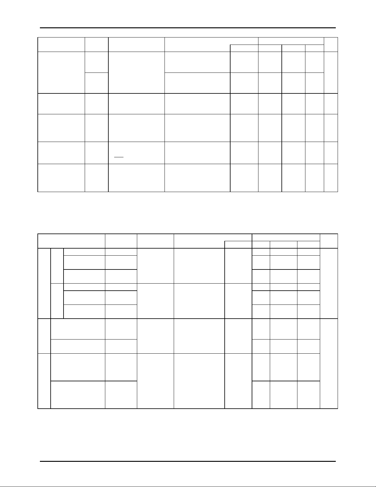
Parameter Symbol Pins Conditions
IOFF(1) •Output P-channel
leakage current
IOFF(2)
•S0/T0 to S6/T6
•S28 to S37
(without pull-down
resistor)
Tr. OFF
•VOUT=VSS
•Output P-channel
Tr. OFF
•VOUT=VDD-40V
‘L’ level hold Tr.
of high voltage
Rinpd S16 to S37 Output P-channel
Tr. OFF
withstand input
pull-down
transistor resistor
Hysteresis
voltage
Rpd •S7/T7 to S15/T15
•S16 to S27
(without pull-down
resistor)
VHIS •Port 1
•Ports 70,71,72,73
RES
•
•Output P-channel
Tr. OFF
•VOUT=3V
•Vp=-30V
Output disable 4.5 to 6.0 0.1VDD V
Pin capacitance CP All pins •f=1MHz
•VIN=VSS for all
unmeasured terminals.
•Ta=25°C
4. Serial Input/output Characteristics at Ta=-30°C to +70°C, VSS1=VSS2=0V
Parameter Symbol Pins Conditions
Cycle tCKCY(1) 2
Low Level
tCKL(1) 1
SCK0,S CK1 Refer to figure 5 4.5 to 6.0
VDD[V] min. typ. max.
pulse width
High Level
Input clock
pulse width
Cycle tCKCY(2) 2
Serial clock
Low Level
pulse width
High Level
Output clock
pulse width
Data set-up time
Data hold time
Serial input
Output delay time
(External clock
using for serial
transfer clock)
Output delay time
(Internal clock
Serial output
using for serial
tCKH(1)
SCK0,SCK1 •Use pull-up
tCKL(2) 1/2tCKCY
resistor (1kΩ)
4.5 to 6.0
in the open drain
tCKH(2)
output.
•Refer to figure 5
tICK 0.1
•SI0,SI1
•SB0,SB1
•Data set-up to
SCK0,1
4.5 to 6.0
•Data hold from
tCKI
SCK0,1
•Refer to figure 5
tCKO(1) 7/12
•SO0,SO1
•SB0,SB1
•Use pull-up
resistor (1kΩ) in
4.5 to 6.0
the open drain
output.
tCKO(2)
•Data hold from
SCK0,1
•Refer to figure 5
transfer clock)
Ratings
VDD[V] min. typ. max.
4.5 to 6.0 -1 Output off-
unit
A
µ
4.5 to 6.0 -30
4.5 to 6.0 400
5.0 60 100 200
kΩ
kΩ
4.5 to 6.0 10 pF
Ratings
unit
tCYC
1
1/2tCKCY
s
µ
0.1
tCYC
+0.2
1/3
tCYC
+0.2
No.6689-14/22
Page 15
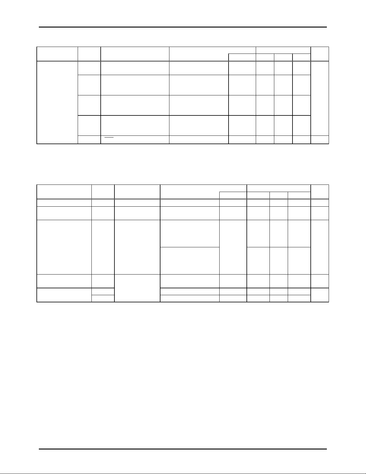
LC86P6449
5. Pulse Input Conditions at Ta=-30°C to +70°C, VSS1=VSS2=0V
Parameter Symbol Pins Conditions
High/low level
pulse width
tPIH(1)
tPIL(1)
tPIH(2)
tPIL(2)
•INT0, INT1
•INT2/T0IN
INT3/T0IN
(The noise rejection clock
•Interrupt acceptable
•Timer0-countable
•Interrupt acceptable
•Timer0-countable
Ratings
VDD[V] min. typ. max.
4.5 to 6.0 1
4.5 to 6.0 2
unit
tCYC
selected to 1/1.)
tPIH(3)
tPIL(3)
INT3/T0IN
(The noise rejection clock
•Interrupt acceptable
•Timer0-countable
4.5 to 6.0 32
selected to 1/16.)
tPIH(4)
tPIL(4)
INT3/T0IN
(The noise rejection clock
•Interrupt acceptable
•Timer0-countable
4.5 to 6.0 128
selected to 1/64.)
tPIL(5)
RES
Reset acceptable 4.5 to 6.0 200
µs
6. AD Converter Characteristics at Ta=-30°C to + 70°C, VSS1=VSS2=0V
Parameter Symbol Pins Conditions
Ratings
VDD[V] min. typ. max.
unit
Resolution N 4.5 to 6.0 8 bit
Absolute precision
ET 4.5 to 6.0 ±1.5 LSB
(Note 2)
Conversion time tCAD
AD conversion time =
16 × tCYC
(ADCR2=0)
4.5 to 6.0
68
15.
(tCYC=
0.98µs)
65.28
(tCYC=
4.08µs)
µs
(Note 3)
AD conversion time =
32 × tCYC
(ADCR2=1)
31.36
(tCYC=
0.98µs)
130.56
(tCYC=
4.08µs)
(Note 3)
Analog input
VAIN 4.5 to 6.0 VSS VDD V
AN0 to AN7
voltage range
input current
IAINH VAIN=VDD 4.5 to 6.0 1 Analog port
IAINL
VAIN=VSS 4.5 to 6.0 -1
A
µ
(Note 2) Absolute precision excepts the quantizing error (±1/2 LSB).
(Note 3) The conversion time means the time from executing the AD conversion instruction to setting the complete digital
conversion value to the register.
No.6689-15/22
Page 16
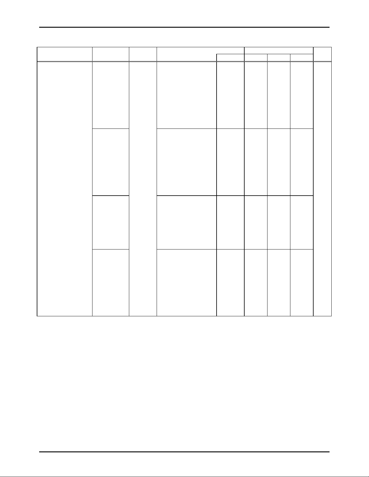
LC86P6449
7. Current Dissipation Characteristics at Ta=-30°C to +70°C, VSS1=VSS2=0V
Parameter Symbol Pins Conditions
Current dissipation
during basic
operation
(Note 4)
IDDOP(1) •FmCF=6MHz
Ceramic resonator
oscillation
•FsXtal=32.768kHz
Ratings
VDD[V] min. typ. max.
4.5 to 6.0 14 33
crystal oscillation
•System clock :
CF oscillation
•Internal RC
oscillation stops
•1/1 divided
IDDOP(2) •FmCF=3MHz
4.5 to 6.0 6 18
Ceramic resonator
oscillation
•FsXtal=32.768kHz
crystal oscillation
•System clock :
CF oscillation
•Internal RC
oscillation stops
•1/2 divided
IDDOP(3) •FmCF=0Hz
4.5 to 6.0 4 13
(The oscillation
stops)
•FsXtal=32.768kHz
crystal oscillation
•System clock :
RC oscillation
•1/2 divided
IDDOP(4)
•FmCF=0Hz
4.5 to 6.0 3 10
(The oscillation
stops)
•FsXtal=32.768kHz
crystal oscillation
•System clock :
32.768kHz
•Internal RC
oscillation stops
•1/2 divided
Continue.
unit
mA
No.6689-16/22
Page 17

LC86P6449
Parameter Symbol Pins Conditions
Current dissipation
in HALT mode
(Note 4)
IDDHALT(1) •HALT mode
•FmCF=6MHz
Ceramic resonator
Ratings
VDD[V] min. typ. max.
4.5 to 6.0 5 14
oscillation
•FsXtal=32.768kHz
crystal oscillation
•System clock :
CF oscillation
•Internal RC
oscillation stops
•1/1 divided
IDDHALT(2) •HALT mode
4.5 to 6.0 2.2 7
•FmCF=3MHz
Ceramic resonator
oscillation
•FsXtal=32.768kHz
crystal oscillation
•System clock :
CF oscillation
•Internal RC
oscillation stops
•1/2 divided
IDDHALT(3) •HALT mode
4.5 to 6.0 400 1600
FmCF=0Hz
(The oscillation
stops)
•FsXtal=32.768kHz
crystal oscillation
•System clock :
RC oscillation
•1/2 divided
IDDHALT(4)
•HALT mode
4.5 to 6.0 25 100
FmCF=0Hz
(The oscillation
stops)
•FsXtal=32.768kHz
crystal oscillation
•System clock :
crystal oscillation
•Internal RC
oscillation stops
•1/2 divided
Current dissipation
in HOLD mode
IDDHOLD(1) HOLD mode
4.5 to 6.0 0.05 30
(Note 4)
(Note 4) The currents of the output transistors and the pull-up MOS transistors are ignored.
unit
mA
µA
No.6689-17/22
Page 18
LC86P6449
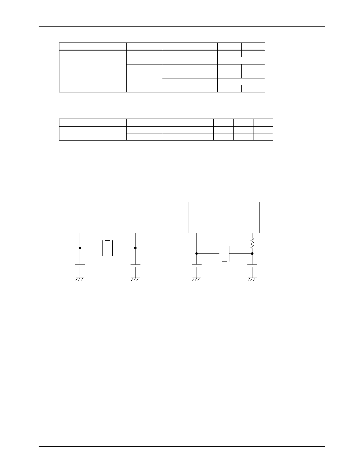
Table 1. Ceramic resonator oscillation recommended constant (main-clock)
Oscillation type Maker Oscillator C1 C2
6MHz ceramic resonator
oscillation
Murata
on chip
Kyocera
3MHz ceramic resonator
oscillation
Murata
on chip
Kyocera
* Both C1 and C2 must be use K rank (±10%) and SL characteristics.
Table 2. Crystal oscillation guaranteed constant (sub-clock)
Oscillation type Maker Oscillator C3 C4 Rd
32.768kHz crystal
oscillation
* Both C3 and C4 must be use J rank (±5%) and CH characteristics.
(Not in need of high precision, use K rank (±10%) and SL characteristics.)
(Notes) • Please place the oscillation-related parts as close to the oscillation pins as possible with the shortest
possible pattern length since the circuit pattern affects the oscillation frequency.
• If you use other oscillators herein, we provide no guarantee for the characteristics.
CF1 CF2
XT1 XT2
Rd
CF
C2 C1
X’tal
C4 C3
Figure 1 Main-clock circuit Figure 2 Sub-clock circuit
Ceramic resonator oscillation Crystal oscillation
No.6689-18/22
Page 19
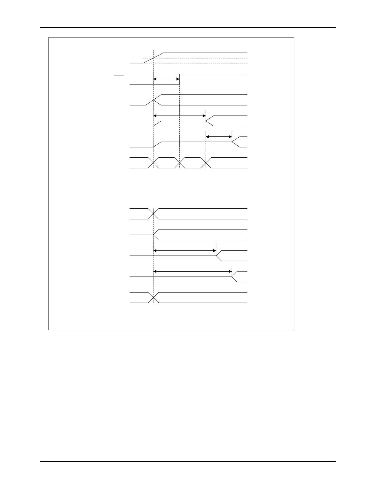
LC86P6449
I
Power supply
RES
Reset time
VDD
VDD limit
0V
resonator oscillation
Internal RC
tmsCF
CF1, CF2
tssXtal
XT1, XT2
Operation mode
Unfixed
Reset
nstruction
execution
mode
OCR6=1
Instruction execution mode
<Reset time and oscillation stable time>
HOLD release signal
Valid
resonator oscillation
Internal RC
tmsCF
CF1, CF2
tssXtal
XT1, XT2
Operation mode
HOLD
Instruction execution mode
<HOLD release signal and oscillation stable time>
Figure 3 Oscillation stable time
No.6689-19/22
Page 20
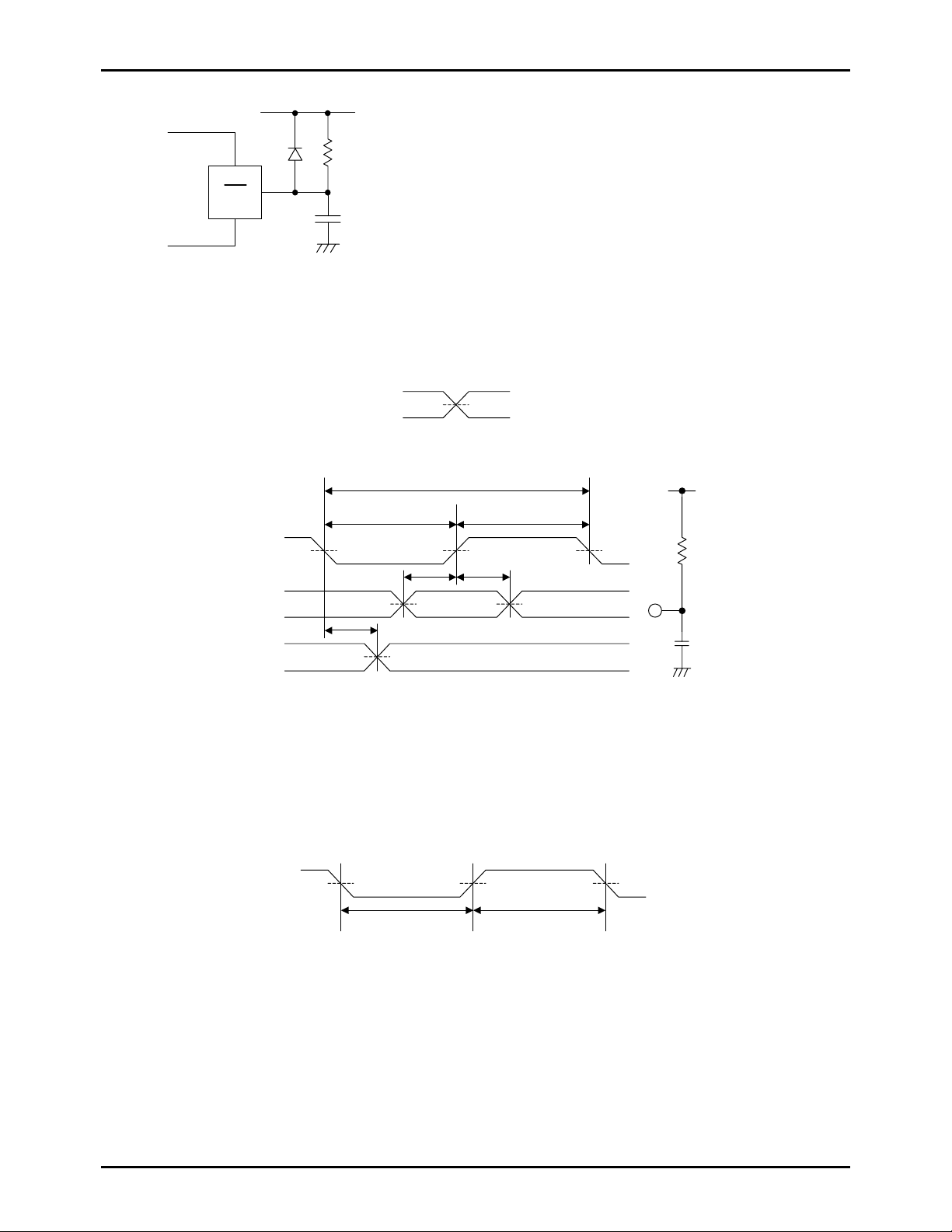
LC86P6449
VDD
RES
R
RES
(Note) Fix the value of CRES, RRES that is
sure to reset until 200µs, after Power
supply has be en over inferior limit of
RES
C
supply voltage.
Figure 4 Reset circuit
<AC timing point>
0.5VDD
tCKCY
VDD
SCK0
SCK1
SI0
SI1
SO0, SO1
SB0, SB1
tCKL tCKH
tICK tCKI
tCKO
<Timing>
1kΩ
50pF
<Test load>
Figure 5 Serial input / output test condition
tPIL tPIH
Figure 6 Pulse input timing condition
No.6689-20/22
Page 21
LC86P6449
Notice for use
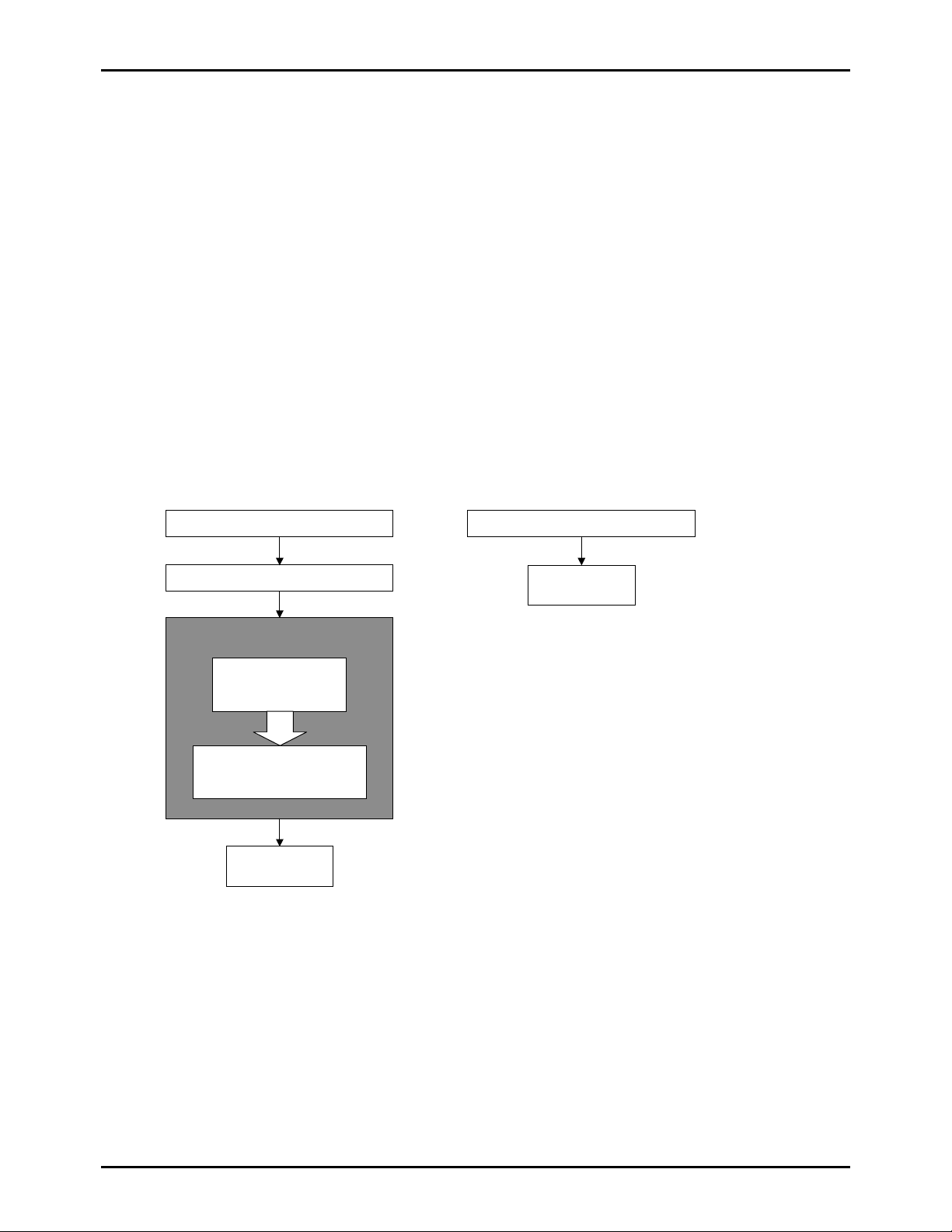
The construction of the one-time programmable microcomputer with a blank built-in PROM makes it impossible for Sanyo to
•
completely factory-test it before shipping. To probe reliability of the programmed devices, the screening procedure shown
in the following figure should always be followed.
It is not possible to perform a writing test on the blank PROM. 100% yield, therefore, cannot be guaranteed.
•
Keeping the dry packing
•
The environment must be held at a temperature of 30°C or less and a humidity level of 70% or less.
After openi ng the packing
•
The preparation procedures shown in the following figure should always be followed prior to mounting the packages on the
substrate. After opening the packing, a controlled environment must be maintained until soldering. The environment
must be held at a temperature of 30°C or less and a humidity level of 70% or less. Please solder within 96 hours.
Unused devices should be kept in the dry atmosphere such as inside of desiccator or dry these up before assembling on the
board.
a. Shipping with a blank PROM b. Shipping with a programmed PROM
(Programming the data by yourself) (Programming the data by Sanyo)
Writing data for program/Verifying
Recommended process of screening
Reading ascertation of program
DIP
Heat-soak
Mounting
+1
-0
150±5°C, 24 Hr
VDD=5±0.5V
QFP
Mounting
No.6689-21/22
Page 22

memo:
LC86P6449
No.6689-22/22
PS
 Loading...