

SANYO LC875064B, LC875048B Datasheet

Ordering number : ENN*6714
CMOS IC
LC875064B/56B/48B
8-Bit Single Chip Microcontroller with
64/56/48K-By te EP ROM an d 20 48- Byte RAM On Chip
Preliminary
Overview
The LC875064B/56B/48B microcontroller is 8-bit single chip microcontroller with the following on-chip functional blocks:
- CPU: Operable at a minimum bus cycle time of 100ns
- 64K/56K/48K bytes ROM
- 2048 byte RAM
- two high performance 16 bit timer/counters (can be divided into 8 bit units)
- two 8 bit timers with prescalers
- timer for use as date/time clock
- one synchronous serial I/O ports (with automatic block transmit/receive function)
- one asynchronous/synchronous serial I/O port
- 12-bit PWM × 2
- 3-channel × 8-bit AD converter
- high speed 8-bit parallel interface
- 16-sour ce 10-vec tored interrupt system
All of the above functions are fabricated on a single chip.
Features
(1) Read Only Memory (ROM)
- 65535 × 8 bits (LC875064B)
- 57343 × 8 bits (LC875056B)
- 49151 × 8 bits (LC875048B)
Ver.1.03
12500
91400 RM (IM) HK / SY No.6714-1/26

LC875064B/56B/48B
(2) Random Access Memory (RAM)
- 2048 × 8 bits (LC875064B/56B/48B)
(3) Bus Cycle Time
- 100ns (10MHz)
Note: The bus cycle time indicates ROM read time.
(4) Minimum Instruction Cycle Time : 300ns (10MHz)
(5) Ports
- Input/output ports
Each bit data direction programmable 51 (P1n, P2n, P70 to P73, P80 to P82, PA2 to PA5,
PBn, PCn)
Nibble data direction programmable 8 (P0n)
- Input ports 2 (XT1,XT2)
- PWM Output po rts 2 (PWM0,PWM1)
- Oscillator pins 2 (CF1,CF2)
- Reset pin 1 (
RES)
- Power supply 6 (VSS1 to 3,VDD1 to 3)
(6) Timers
- Timer0: 16 bit timer/counter with capture register
Mode 0: 2 channel 8 bit timer with programmable 8 bit prescaler and 8 bit capture register
Mode 1: 8 bit timer with 8 bit programmable prescaler and 8 bit capture register + 8 bit counter with 8 bit
capture register
Mode 2: 16 bit timer with 8 bit programmable prescaler and 16 bit capture register
Mode 3: 16 bit counter with 16 bit capture register
- Timer1: PWM/16 b it timer/counter (with togg le output)
Mode 0: 8 bit timer (with toggle output) + 8 bit timer counter (with toggle output)
Mode 1: 2 channel 8 bit PWM
Mode 2 : 1 6 bit timer/counter (wit h toggle outp ut)
Mode 3: 16 bit timer (with toggle output) Lower order 8 bits can be used as PWM output.
- Base timer
1. The clock signal can be selected from any of the following: sub-clock (32.768kHz crystal oscillator), system
clock, and prescaler output for timer 0.
2. Interrupts can be selected to occur at one of five different times.
(7) SIO
- SIO0: 8 bit synchronous serial interface
1. LSB first/MSB first function available
2. Internal 8-bit baud-rate generator (maximum transmit clock period 4/3 T
3. Continuous automatic data communications (1 - 256 bits)
- SIO1: 8 bit asynchronous/synchronous serial interface
Mode 0: Synchronous 8 bit serial IO (2-wire or 3-wire, transmit clock 2 - 512 T
Mode 1: Asynchronous serial IO (half duplex, 8 data bits, 1 stop bit, baud rate 8 - 2048 T
Mode 2: Bus mode 1 (start bit, 8 data bits, transmit clock 2 - 512 T
Mode 3: Bus mode 2 (start detection, 8 data bits, stop detection)
(8) AD converter
- 8-bits × 3-channels
(9) PWM
- 2 channel synchronous variable 12 bit PWM
(10) Parallel interface
- RS,
RD , WR , CS0 - CS2 Outputs (reversible polarity)
- read/write possible in 1 T
CYC
CYC
)
CYC
)
CYC
)
CYC
)
No.6714-2/26
LC875064B/56B/48B
(11) Remote control receiver circuit (connected to P73/INT3/T0IN terminal)
- Noise rejection function (noise rejection filter time constant can selected from 1/32/128 T
(12) Watchdog timer
- The watchdog timer period set by external RC.
- Watchdog timer can be set to produce interrupt, system reset
(13) Interrupts
- 16-source, 10-vectored interrupts:
1. Three level (low, high and highest) multiple interrupts are supported. During interrupt handling, an equal or
lower level interrupt request is refused.
2. If interrupt requests to two or more vector addresses occur at once, the higher level interrupt takes precedence.
In the case of equal priority levels, the vector with the lowest address takes precedence.
No. Vector Selectable Level Interrupt signal
1 00003H X or L INT0
2 0000BH X or L INT1
3 00013H H or L INT2/T0L/INT4
4 0001BH H or L INT3/INT5/Base timer
5 00023H H or L T0H
6 0002BH H or L T1L/T1H
7 00033H H or L SIO0
8 0003BH H or L SIO1
9 00043H H or L ADC
10 0004BH H or L Port 0/PWM0, 1
• Priority Lev el: X > H > L
• For equal priority levels, vector with lowest address takes precedence.
(14) Subroutine stack levels
- 1024 levels max. Stack is located in RAM
(15) Multiplication and division
- 16 bit × 8 bit (executed in 5 cycles)
- 24 bit × 16 bit (12 cycles )
- 16 bit ÷ 8 bit (8 cycles)
- 24 bit ÷ 16 bit (12 cycles)
(16) Oscillation circuits
- On-chip RC oscillation circuit used for system clock
- On-chip CF oscillation circuit used for system clock
- On-chip Crystal oscillation circuit used for system clock and time-base clock
(17) Standby function
- HALT mode
HALT mode is used to reduce power consumption. Program execution is stopped. Peripheral circuits still operate.
1. Oscillation circuits are not stopped automatically
2. Release on system reset
- HOLD mode
HOLD mode is used to reduce the power dissipation. Both program execution and peripheral circuits are stopped.
1. CF, RC and crystal oscillation circuits stop automatically
2. Release occurs on any of the following conditions
•input to the reset pin goes low
•a specified level is input to at least one of INT0, INT1, INT2, INT4, INT5
•an interrupt condition arises at port 0
CYC
)
No.6714-3/26

LC875064B/56B/48B
- X’tal HOLD mode
X’tal HOLD mode is used to reduce power consumption. Program execution is stopped. All peripheral circuits
except the base timer are stopped.
1. CF and RC oscillation circuits stop automatically
2. Crystal oscillator is maintained in its state at HOLD mode inception.
3. Release occurs on any of the following conditions
•input to the reset pin goes low
•a specified level is input to at least one of INT0, INT1, INT2, INT4, INT5
•an interrupt condition arises at port 0
•an interrupt condition arises at the base-timer
(18) Factory shipment
- delivery form QIP64E
- delivery form DIP64S
(19) Development Tools
- Evaluation chip : LC876098
- Emulator : EVA87000 + ECB875000 (Evaluation chip board) + POD875000 (POD)
No.6714-4/26
Pin Assignment
L
Z
P70/INT0/T0LCP
P71/INT1/T0HCP
P72/INT2/T0IN
P73/INT3/T0IN
RES#
XT1
XT2
VSS1
CF1
CF2
VDD1
P80/AN0
P81/AN1
P82/AN2
P10/SO0
P11/SI0/SB0
Package Dimension
(unit : mm)
3159
PA5/RS
PA4/RD#
PA3/WR#
48
47 46 45 44 43 42 41 40 39 38 37 36 35 34 33
49
50
51
52
53
54
55
56
57
58
59
60
61
62
63
64
1 2 3 4 5 6 7
P12/SCK0
LC875064B/56B/48B
P13/SO1
P14/SI1/SB1
LC875064B/56B/48B
PA2/CS0#
PC0/A0
PC1/A1
PC2/A2
PC3/A3
PC4/A4
QIP
8 9 10 11 12 13 14 15
VDD2
PWM1
PWM0
P15/SCK1
P16/T1PWM
P17/T1PWMH/BU
PC5/A5
VSS2
PC6/A6
PC7/A7
VDD3
VSS3
PB0/D0
PB1/D1
32
PB2/D2
31
PB3/D3
30
PB4/D4
29
PB5/D5
28
PB6/D6
27
PB7/D7
26
P27/INT5/T1IN
25
P26/INT5/T1IN
24
P25/INT5/T1IN
23
P24/INT5/T1IN
22
P23/INT4/T1IN
21
P22/INT4/T1IN
20
P21/INT4/T1IN
19
P20/INT4/T1IN
18
P07
17
P06
16
P00
P01
P02
P03
P04
P05
SANYO : QIP-64E
No.6714-5/26
LC875064B/56B/48B
QIP NAME QIP NAME
1 P12/SCK0 33 PB1/D1
2 P13/SO1 34 PB0/D0
3 P14/SI1/SB1 35 VSS3
4 P15/SCK1 36 VDD3
5 P16/T1PWML 37 PC7/A7
6 P17/T1PWMH/BUZ 38 PC6/A6
7 PWM1 39 PC5/A5
8 PWM0 40 PC4/A4
9 VDD2 41 PC3/A3
10 VSS2 42 PC2/A2
11 P00 43 PC1/A1
12 P01 44 PC0/A0
13 P02 45 PA2/CS0#
14 P03 46 PA3/WR#
15 P04 47 PA4/RD#
16 P05 48 PA5/RS
17 P06 49 P70/INT0/T0LCP
18 P07 50 P71/INT1/T0HCP
19 P20/INT4/T1IN 51 P72/INT2/T0IN
20 P21/INT4/T1IN 52 P73/INT3/T0IN
21 P22/INT4/T1IN 53 RES#
22 P23/INT4/T1IN 54 XT1
23 P24/INT5/T1IN 55 XT2
24 P25/INT5/T1IN 56 VSS1
25 P26/INT5/T1IN 57 CF1
26 P27/INT5/T1IN 58 CF2
27 PB7/D7 59 VDD1
28 PB6/D6 60 P80/AN0
29 PB5/D5 61 P81/AN1
30 PB4/D4 62 P82/AN2
31 PB3/D3 63 P10/SO0
32 PB2/D2 64 P11/SI0/SB0
No.6714-6/26
System Bl ock Diagram
SIO0
SIO1
Timer 0
Timer 1
PWM0
PWM1
Base Timer
Interrupt control
Standby control
CF
RC
Xtal
Clock
LC875064B/56B/48B
Generator
Bus Interface
Port 0
Port 1
Port 7
Port 8
ADC
INT0-3
Noise Rejection Filter
Port 2 INT4,,5
Parallel interface
Port A
Port B
Port C
IR PLA
ROM
PC
ACC
B Register
C Register
ALU
PSW
RAR
RAM
Stack Pointer
Watch Dog Timer
No.6714-7/26
LC875064B/56B/48B
Pin Assignment
Pin Name I/O Pin Function Option
VSS1
VSS2
VSS3
VDD1
VDD2
VDD3
Port 0
P00 - P07
Port 1
P10 - P17
Port 2 •8-bit Input/output port
P20 - P27
- Negative power supply No
- Positive power supply No
I/O •8-bit Input/output port
•Data direction can be specified in nib ble units
•Use of pull-up resistor can be specified in nibble units
•HOLD-release input
•Input for port 0 interrupt
I/O •8-bit Input/output port
•Data direction can be specified for each bit
•Use of pull-up resistor can be specified for each bit
•Other functions
P10: SIO0 data output
P11: SIO0 data input/bus input/output
P12: SIO0 clock input/output
P13: SIO1 data output
P14: SIO1 data input/bus input/output
P15: SIO1 clock input/output
P16: Timer 1 PWML output
P17: Timer 1 PWMH output/Buzzer output
I/O
•Data direction can be specified for each bit
•Use of pull-up resistor can be specified for each bit
•Other functions
P20-P23: INT4 input/HOLD release input/timer 1 event input
/Timer 0L capture input/Timer 0H capture input
P24-P27: INT5 input/HOLD release input/timer 1 event input
/Timer 0L capture input /Timer 0H capture input
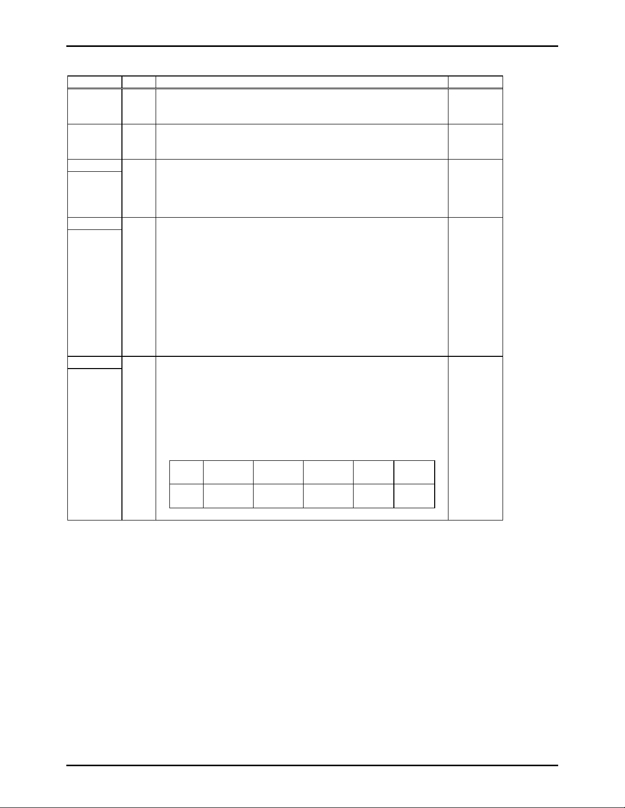
Interrupt receiver format
Rising Falling Rising/
INT4
INT5
Yes
Yes
Yes
Yes
falling
Yes
Yes
H level L level
No
No
No
No
Yes
Yes
Yes
(Continued)
No.6714-8/26
 Loading...