

SANYO LC86P7248 Datasheet

Ordering number : ENN*6838
LC86P7248
8-Bit Single-Chip Microcontroller
with the One-Time Programmable PROM Built in
Preliminary
Overview
The LC86P7248 is a CMOS 8-bit single chip microcontroller with one-time PROM for the LC867200 series. This
microcontroller has the function and the pin description of the LC867200 series mask ROM version, and 48K-byte
EPROM.
QIP package are available for shipping as well as LC867200 series. It is suitable to set up first release, prototyping,
developing and testing of set.
Features
(1) Option switching by PROM data
The option function of the LC867200 series can be specified by the PROM data.
LC86P7248 can be checked the functions of the trial pieces using the mass production board.
(2) Internal one-time PROM capacity : 49408 bytes
(3) Internal RAM capacity : 1152 bytes
Used PROM or RAM capacity are equal ROM or RAM capacity of mask ROM version which applies LC86P7248.
Mask ROM version EPROM capacity RAM capacity
LC867248 49152 bytes 1152 bytes
LC867240 40960 bytes 1152 bytes
LC867232 32768 bytes 1152 bytes
LC867224 24576 bytes 1152 bytes
Programming service
We offers various services at nominal charges. These include ROM writing, ROM reading and package stamping and
screening. Contact local our representative for further information.
CMOS IC
Ver.1.02
72396
D2700 RM (IM) SK No.6838-1/20

LC86P7248
(4) Operating supply voltage : 4.5V to 6.0V
(5) Instruction cycle time : 1µs to 366µs
(6) Operating temperature : -30°C to +70°C
(7) The pin compatible with the LC867200 series mask ROM devices
(8) Applicable mask ROM version : LC867248/LC867240/LC867232/LC867224
(9) Factory shipment : QIP100E
Notice for use
LC86P7248 is provided for the first release and small shipping of the LC867200 series.
At using, take notice of the followings.
(1) A point of difference LC86P7248 and LC867200 series
Item LC86P7248 LC867248/40/32/24
Operation after reset
releasing
Operating supply
voltage range (VDD)
Power dissipa tion Refer to ‘electrical characteristics’ on the semiconduct or news.
The option is specified until 3ms after
going to a ‘H’ level to the reset
terminal by degrees. The program is
executed from 00H of the program
counter.
4.5V to 6.0V 2.5V to 6.0V
LC86P7248 uses 256 bytes that is addressed on 0FF00H to FFFFH in the program memory as the option configuration data
area. This option configuration can execute all options which LC867200 series have.
• A kind of the option of the LC86P7248
A kind of option Pins, Circuits Contents of the option
Input/output form of
input/output ports
Pull-up MOS Tr. of
input port
Port 0
Port 1
*1
Port 3
*1
Ports 70, 71, 72, 73
*1
1. N-channel open drain output
2. CMOS output *1
1. Pull-up MOS Tr.
2. No Pull-up MOS Tr. *2
1. Input : Programmable pull-up MOS Tr.
2. Input : Programmable pull-up MOS Tr.
Output : CMOS
1. Input : No Programmable pull-up MOS Tr.
2. Input : Programmable pull-up MOS Tr.
Output : CMOS
1. No Pull-up MOS Tr.
2. Pull-up MOS Tr.
*1) Specified in a bit.
*2) Specified in nibble unit. Pull-up MOS Tr. is not provided in N-channel open drain output port.
The program is executed from 00H of
the program counter i mmediately after
going to a ‘H’ level to the reset
terminal.
Output : N-channel open drain
Output : N-channel open drain
No.6838-2/20
LC86P7248
(1) Option
The option data is created by the option specified program “SU86K.EXE”. The created option data is linked to the
program area by linkage loader “L86K.EXE” .
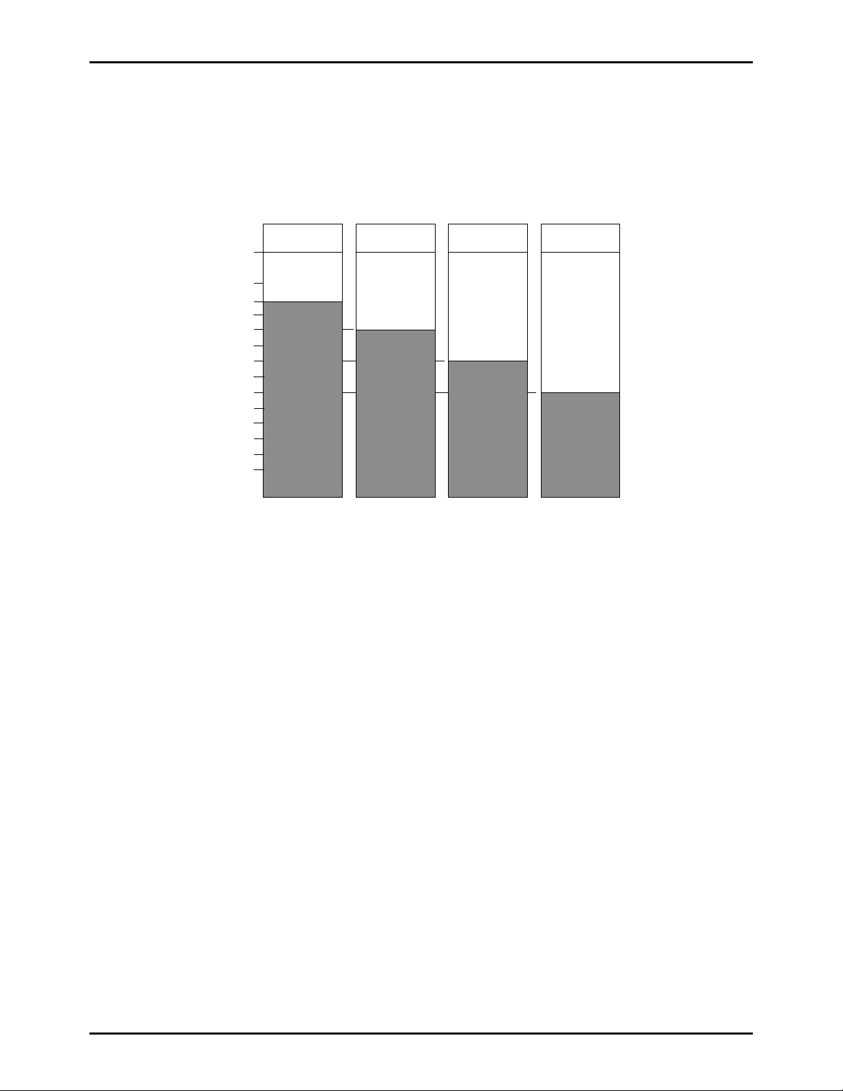
(2) ROM space
LC86P7248 and LC8672 00 series use 256 bytes that is addresse d on 0FF00H to 0 FFFFH in the program memory as the
option specified data area. These program memory capacity are 49152 bytes that is addressed on 0000H to 0BFFFH.
0FFFFH
0FF00H
0EFFFH
0DFFFH
0CFFFH
0BFFFH
0AFFFH
9FFFH
8FFFH
7FFFH
6FFFH
5FFFH
4FFFH
3FFFH
2FFFH
1FFFH
0FFFH
0000H
Option data
area 256 bytes
Option
data area
Program area
48K bytes
LC867248 LC867240
Program area
40K bytes
Option
data area
Program area
32K bytes
LC867232
Option
data area
Program area
24K bytes
LC867224
(3) Ordering information
1. When ordering the identical mask ROM and PROM devices simultaneously.
Provide an EPROM containing the target memory contents together with the separate order forms for each of the mask
ROM and PROM versions.
2. When ordering a PROM device.
Provide an EPROM containing the target memory contents together with an order form.
No.6838-3/20
LC86P7248
How to use
(1) Specification of option
Programming data for PROM of the LC86P7248 is required.
Debugged evaluation file (EVA file) must be converted to an INTEL-HEX formatted file (HEX file) with file converter
program, EVA2HEX.EXE. The HEX file is used as the programming data for the LC86P7248.
(2) How to program for the PROM
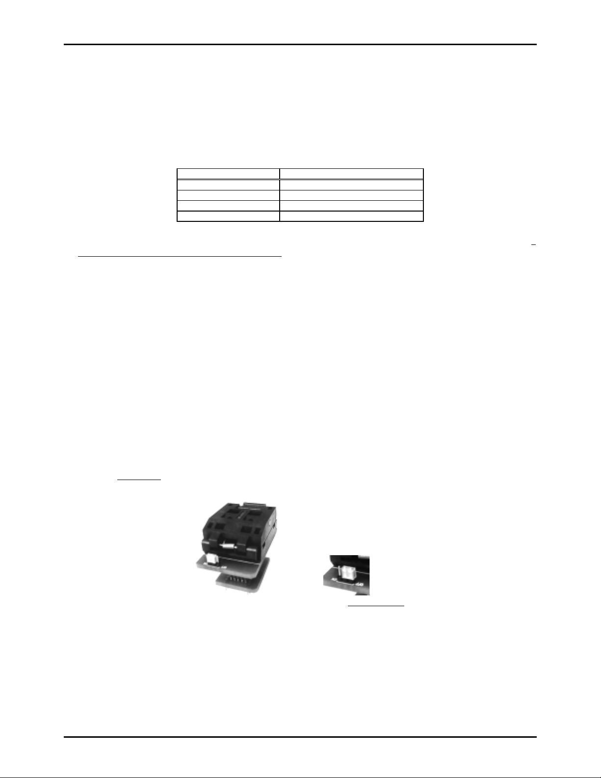
The LC86P7 248 can be prog rammed by PROM programmer with attac hment ; W86EP7248Q
• Recommended EPROM programmer
Productor EPROM programmer
Advantest R4945, R4944, R4943
Andou AF-9704
AVAL PKW-1100, PKW-3000
Minato electronics MODEL1890A
• “27512 (Vpp=12.5V) Intel high speed programming” mode available. The address must be set to “0 to 0FFFFH” and a
jumper (DASEC) must b e set to ‘OFF’ at programming.
(3) How to use the data security function
“Data security” is the disabled function to read the data of the PROM.
The following is the process in order to execute the data security.
1. Set ‘ON’ the jumper of attachment.
2. Program again. Then PROM programmer displays the error. The error means normally activity of the data security.
It is not a trouble of the PROM programmer or the LSI.
Notes
• Data security is not executed when the data of all address have ‘FFH’ at the sequence 2 above.
• The programming by a sequential operation “BLANK=>PROGRAM=>VERIFY” cannot be executed data security at the
sequence 2 above.
• Set to ‘OFF’ the jumper after executing the data security.
Data security
W86EP7248Q
Not data security
No.6838-4/20

Pin Assignment
V3/PL6
S47/PF7
S46/PF6
S45/PF5
S44/PF4
S43/PF3
S42/PF2
S41/PF1
S40/PF0
LC86P7248
S39/PE7
S38/PE6
S37/PE5
S36/PE4
S35/PE3
S34/PE2
S33/PE1
S32/PE0
S31/PD7
S30/PD6
S29/PD5
S28/PD4
S27/PD3
S26/PD2
VSS2
VDD2
S25/PD1
S24/PD0
S23/PC7
S22/PC6
S21/PC5
V2/PL5
V1/PL4
COM0/PL0
COM1/PL1
COM2/PL2
COM3/PL3
P30
P31
VSS3
VDD3
P32
P33
P34
P35
P00
P01
P02
P03
P04
P05
8079787776757473727170696867666564636261605958575655545352
81
82
83
84
85
86
87
88
89
90
91
92
93
94
95
96
97
98
99
100
123456789
P06
P07
P10/SO0
P13/SO1
P12/SCK0
P11/SI0/SB0
101112131415161718192021222324252627282930
P16/BUZ
P15/SCK1
P17/PWM0
P70/INT0
P14/SI1/SB1
RES
VSS1
XT1/P74
XT2/P75
CF1
CF2
VDD1
P80/AN0
P81/AN1
P82/AN2
P83/AN3
P84/AN4
P85/AN5
P86/AN6
P87/AN7
51
50
49
48
47
46
45
44
43
42
41
40
39
38
37
36
35
34
33
32
31
S0/PA0
P71/INT1
P72/INT2/T0IN
P73/INT3/T0IN
S20/PC4
S19/PC3
S18/PC2
S17/PC1
S16/PC0
S15/PB7
S14/PB6
S13/PB5
S12/PB4
S11/PB3
S10/PB2
S9/PB1
S8/PB0
S7/PA7
S6/PA6
S5/PA5
S4/PA4
S3/PA3
S2/PA2
S1/PA1
Notes
• The QIP packages should be heat-soaked for 12 hours at 125°C immediately prior to mounting (This baking is called
pre-baking).
• After pre-baking, a controlled environment must be maintained until soldering. The environment must be held at a
temperature of 30°C or less and a humidity level of 70% or less. Please solder within 24 hours.
Package Dimension
(unit : mm)
3151
SANYO : QIP-100E
No.6838-5/20
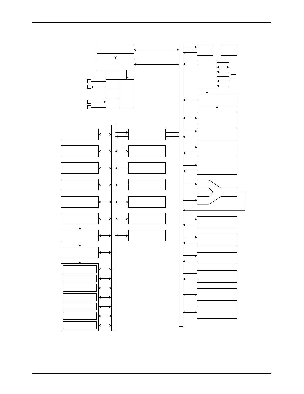
System Bl ock Diagram
LC86P7248
Interrupt Control
Stand-by C ontr ol
CF
RC
X’tal
Base Timer Bus Interface
SIO0
SIO1
Timer 0
Clock
Generator
Port 1
Port 7
Port 8
IR PLA
EPROM
Control
EPROM (48KB)
PC
ACC
B Register
C Register
ALU
A15-A0
D7-D0
TA
CE
OE
DASEC
Timer 1
Real Time Service
RAM 128 bytes
LCD Display
Controller
SO0 to S7 (PA)
S8 to S13 (PB)
S16 to S23 (PC)
S24 to S31 (PD)
S32 to S39 (PE)
S40 to S47 (PF)
COM0 to -COM3(PL)
Port 3
ADC
INT0 to 3 Noise
Rejection Filter
PSW
RAR
RAM
Stack Pointer
Port 0
Watchdog T i mer
No.6838-6/20
 Loading...