

Ordering number : ENN4212A
Overview
The LC86P6032 microcontroller, a new addition to the LC866000 series, is a 8-bit single chip CMOS microcontroller with
one-time PROM. This microcontroller has the same function and pin assignment as for the LC866000 series mask ROM
version, and a 32K-byte PROM.
Features
(1) Option switching using PROM data
The optional functions of the LC866000 series can be specified using PROM data.
The functions of the trial products can be evaluated using a mass production board.
(2) Internal one-time PROM capacity : 32768 bytes
(3) Internal RAM capacity : 512 bytes
Mask ROM version PROM capacity RAM capacity
LC866032
LC866028
LC866024
LC866020
LC866016
LC866012
LC866008
(4) Operating supply voltage : 4.5V to 6.0V
(5) Instruction cycle time : 0.98µs to 400µs
(6) Operating temperature range : -30°C to +70°C
(7) Pin and package compatible with the mask ROM version
(8) Applicable mask ROM version : LC866032/LC866028/LC866024/LC866020/LC866016 /LC866 012
/LC866008
(9) Factory shipment : DIP64S
: QFP64E
Programming service
We offer various services at nominal charges. These include ROM writing, ROM reading, and package stamping and
screening. Contact our local representatives for further information.
32512 bytes
28672 bytes
24576 bytes
20480 bytes
16384 bytes
12288 bytes
8192 bytes
CMOS IC
LC86P6032
8-Bit Single Chip Microcontroller
with One-Time PROM
512 bytes
512 bytes
512 bytes
384 bytes
384 bytes
384 bytes
384 bytes
Ver.1.02G
31293
91400 RM (IM) TW No.4212-1/22
LC86P6032
Notice for use
When using, please take note of the following.
(1) Differences between the LC86P6032 and the LC866000 series
Item LC86P6032 LC866032/28/24/20/16/12/08
Port status at reset Please refer to “Port status at reset” on t he next page.
Operation after releasing
reset
Output form of segment
•S0/T0 to S6/T6
•S7/T7 to S15/T15
•S16 to S23
•S24 to S29
Operating supply
voltage range (VDD)
Power dissipation Refer to “electrical characteristics” on the semiconductor news.
LC86P6032 uses 256 bytes that is addressed on 7F00H to 7FFFH in the program memory as the option
configuration data area. This option configuration cannot execute all options which LC866000 series have. Next
tables show the options that correspond and not correspond to LC86P6032.
• LC86P6032 Options
Option Pins, Circuits Option Settings
Configuration of input/output ports Port 0
Port 1
Port 7 pull-up MOS transistor Port 7
• A kind of option not corresponding LC86P6032
Option Pins, Circuits LC86P6032 LC866032/28/24/20/16/12/08
Pull-down resistor of high
voltage withstand output
terminal
The port operation related to the option is different at reset. Please refer to the next table.
The option is speci fied by degrees within
3ms after applying a ‘H’ level to the reset
pin.
The program located at 00H is
executed.
Pulldown resis tor
Not provided
Provided(fixed)
Provided(fixed)
Not provided
4.5V to 6.0V 2.5V to 6.0V
1. Input : No pull-up MOS transistor
(Can be specified for
each bit.)
(Can be specified for
each bit.)
(Can be specified for
each bit.)
·S0/T0 to S6/T6
·S16 to S23
·S24 to S29
(specified in a bit)
Output : N-channel open drain
2. Input : Pull-up MOS transistor
Output : CMOS
1. Input : Programmable pull-up MOS transistor
Output : N-channel open drain
2. Input : Programmable Pull -up MOS transistor
Output : CMOS
1. Pull-up MOS transist or not provided.
2. Pull-up MOS transist or provided.
Not provided
Provided(fixed)
Not provided
The program located at 00H is executed
immediately after applying a ‘H’ level t o
the reset pin.
Pulldown resistor : Provided/Not provided
Specified by the opt ion
Provided(fixed)
Specified by the opt ion
Specified by the opt ion
Specified by the option
Specified by the opt ion
Specified by the opt ion
No.4212-2/22

LC86P6032
• Port configuration at reset
Pin Option settings LC86P6032 LC866032/28/24/20/16/12/08
P0 Input : No pull-up MOS transistor
Output : N-channel open drain
Input : Pull-up MOS transistor
Output : CMOS
(Same as for the mask version) Input mode without pull-up
MOS transistor (Output is OFF)
Input mode
•The Pull-up MOS transistor is
Input mode with pull-up MOS
transistor (Output is OFF)
not present during reset or several
hundred microseconds after
releasing reset. After that, the
pull-up MOS transistor is present.
(Output is OFF)
P1 Input : Programmable pull-up MOS
transistor
(Same as for the mask version) Input mode without pull-up
MOS transistor (Output is OFF)
Output : N-channel open drain
Input : Programmable pull-up MOS
transistor
(Same as for the mask version) Input mode without pull-up
MOS transistor (Output is OFF)
Output : CMOS
P7 Pull-up MOS transistor not
provided
Pull-up MOS transistor pro v i de d Input mode
(Same as for the mask version) Input mode without pull-up
MOS transistor
Input mode with pull-up MOS
•The Pull-up MOS transistor is
transistor
not present during reset or several
hundred microseconds after
releasing reset. After that, the
pull-up MOS transi st or is present.
(2) Option
The option data is created by the option specified program “SU866000.EXE”. The created option data is linked to the
program area by the linkage loader “L866000.EXE”.
(3) ROM space
LC86P6032 and LC86 60 00 seri es use 2 56 b ytes that is a dd resse d o n 07 F00 H to 07 FFFH in t he pro gr am memory as t he
option specified data area. These program memory capacity are 32512 bytes that is addressed on 0000H to 7EFFH.
7FFFH
7F00H
7EFFH
6FFFH
Option data
area 256 bytes
Option
Data Area
Option
Data Area
Option
Data Area
Option
Data Area
Option
Data Area
Option
Data Area
5FFFH
4FFFH
3FFFH
2FFFH
1FFFH
0000H
32K
LC866032
LC86P6032
28K
LC866028
24K
LC866024
20K
LC866020
16K
LC866016
12K
LC866012
8K
LC866008
(4) Ordering information
1.When ordering identical mask ROM and PROM devices simultaneously.
Provide an EPROM containing the target memory contents together with separate order forms for each of the mask
ROM and PROM versions.
2. When ordering a PROM device.
Provide an EPROM containing the target memory contents together with an order form.
No.4212-3/22

LC86P6032
How to use
(1) Specification of option
LC86P6032 is programmed after specifying option data. The option is specified by the SU866000.EXE. The specified
option file and the file created by our macro assembler (M866000.EXE) are linked by our linker (L866000.EXE) which
creates HEX file, then the option code is put in the option specified area (07F00H to 07FFFH) of its HEX file.
(2) How to program for the EPROM
The LC86P6032 can be programmed by an EPR O M programmer with attac hments W86EP6032D and W86EP6032Q.
- Recommended EPROM programmer
Supplier EPROM programmer
Advantest R4945, R4944, R4943
Andou AF-9704
AVAL PKW-1100, PKW-3000
Minato electronics MODEL 1890A
- “27512 (Vpp=12. 5 V) Int el high-sp eed pro gramming” mode availa ble. T he ad dr e ss must be set to “00 00 H to 07 FFFH ”
and the jumper (DASEC) must be set ‘OFF’ at programming
.
(3) How to use the data security function
“Data security” is a function to prevent EPROM data from being read.
Instructions on using the data security function :
1. Set the jumper of attachment “ON”.
2. Attempt to pro gram the E PRO M. The EPROM progr ammer will d isplay an er ror. The error ind icatio n is a result of
normal activity of the data security feature. This is not a problem with the EPROM programmer chip.
(Notes)
• The data security function is not carried out when the data of all addresses contain “FF” at step 2 above.
• Data security cannot be executed when the sequential operation “BLANK=>PROGRAM=>VERIFY” is used at step 2 above.
• Set the jumper “OFF” after execution of data security.
1 pin mark
of LSI
Data security
Data security
1 pin
Not data security Not data security
1 pin
W86EP6032Q W86EP6032D
No.4212-4/22
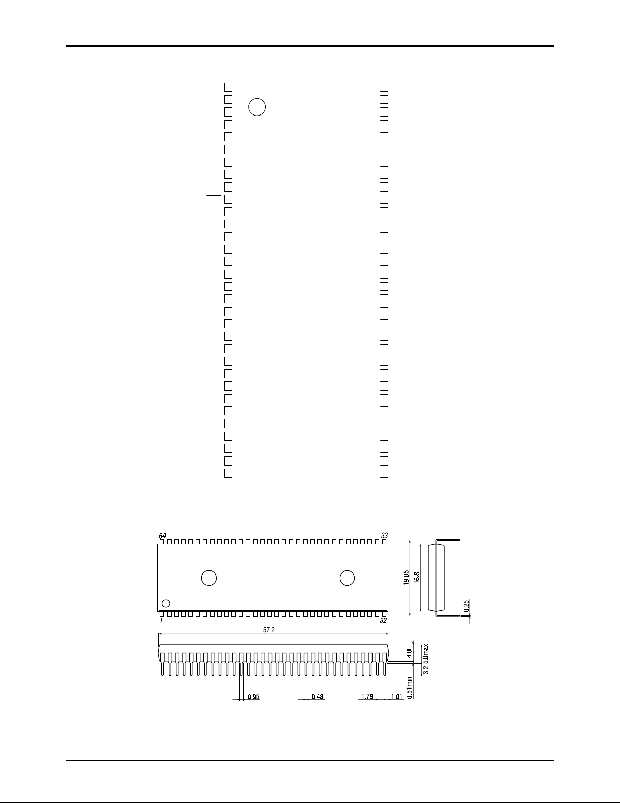
Pin Assignment
Package Dimension
(unit : mm)
3071
P10/SO0
P11/SI0/SB0
P12/SCK0
P13/SO1
P14/SI1/SB1
P15/SCK1
P16/BUZ
P17/PWM
TEST1
RES
XT1
XT2
VSS
CF1
CF2
VDD
P80/AN0
P81/AN1
P82/AN2
P83/AN3
P70/INT0
P71/INT1
72/INT2/T0IN
73/INT3/T0IN
S0/T0
S1/T1
S2/T2
S3/T3
S4/T4
S5/T5
S6/T6
S7/T7
LC86P6032
1
2
3
4
5
6
7
8
9
10
11
12
13
14
15
16
17
18
19
20
21
22
23
24
25
26
27
28
29
30
31
32
64
63
62
61
60
59
58
57
56
55
54
53
52
51
50
49
48
47
46
45
44
43
42
41
40
39
38
37
36
35
34
33
P07
P06
P05
P04
P03
P02
P01
P00
S29
S28
S27
S26
S25
S24
S23
S22
S21
S20
S19
S18
S17
S16
VP
VDDVPP
S15/T15
S14/T14
S13/T13
S12/T12
S11/T11
S10/T10
S9/T9
S8/T8
SANYO : DIP-64S(750mil)
No.4212-5/22

LC86P6032
Pin Assignment
P17/PWM
P16/BUZ
P15/SCK1
P14/SI1/SB1
P13/SO1
P12/SCK0
P11/SI0/SB0
P10/SO0
P07
P06
P05
P04
P03
P02
P01
P00
6
7
8
9
10
11
12
13
14
15
33
32
31
30
29
28
27
26
25
24
23
22
21
20
19
18
17
16
S29
S28
S27
S26
S25
S24
S23
S22
S21
S20
S19
S18
S17
S16
VP
VDDVPP
TEST1
RES
XT1
XT2
VSS
CF1
CF2
VDD
P80/AN0
P81/AN1
P82/AN2
P83/AN3
P70/INT0
P71/INT1
72/INT2/T0IN
73/INT3/T0IN
484746454443424140393837363534
49
50
51
52
53
54
55
56
57
58
59
60
61
62
63
64
1
2
3
4
5
S0/T0
S1/T1
S2/T2
S3/T3
S4/T4
S5/T5
S6/T6
S7/T7
S8/T8
S9/T9
S10/T10
S11/T11
S12/T12
S13/T13
S14/T14
S15/T15
Package Dimension
(unit : mm)
3159
SANYO : QIP-64E
Notes
• The QFP packages should be heat-soaked for 24 hours at 125°C immediately prior to mounting (This baking is called
pre-baking).
• After pre-baking, a controlled environment must be maintained until soldering. The environment must be held at a
temperature of 30°C or less and a humidity level of 70% or less. Please solder within 8 hours.
No.4212-6/22
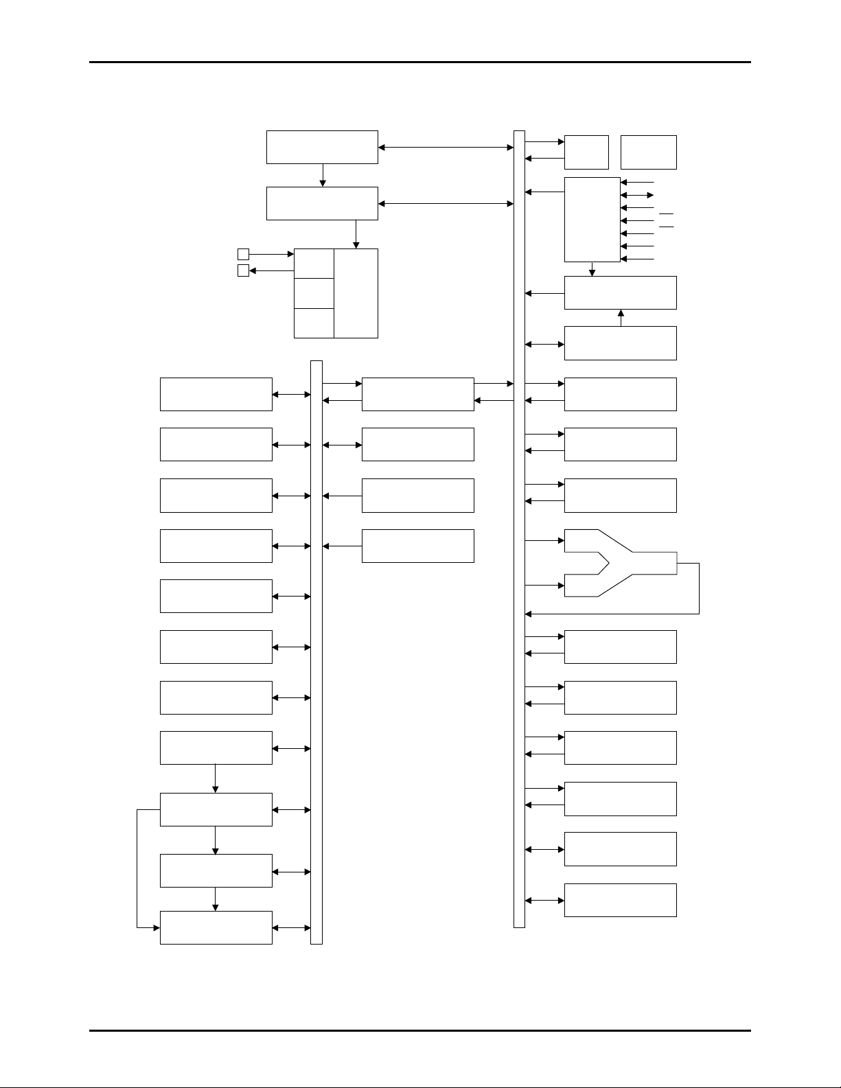
System Bl ock Diagram
Interrupt Control
Stand-by C ontr ol
CF
LC86P6032
IR PLA
PROM
Control
A15-A0
D7-D0
TA
CE
OE
DASEC
VDDVPP
Base Timer
SIO0
SIO1
Timer 0
Timer 1
ADC
RC
X’tal
Clock
Generator
Bus Interface
Port 1
Port 7
Port 8
PROM(32KB)
PC
ACC
B Register
C Register
ALU
PSW
INT0 to 3
Noise Rejec tio n Filte r
Real Time Service
XRAM
(128 bytes)
VFD Controller
High Voltage Output
RAR
RAM
Stack Pointer
Port 0
Watch dog Ti me r
No.4212-7/22
 Loading...