

Page 1
Ordering number: EN5631
LC86P5032
CMOS LSI
LC86P5032
8-Bit Single-Chip Microcontroller
Overview
The LC86P5032 microcontroller, a new addition to the
LC865000 series, is a 8-bit single chip CMOS microcontroller
with one-time PROM.
This microcontroller has the same function and pin assignment
as for the LC865000 series mask ROM version, and a 32K-byte
PROM.
The same DIP/QFP packages as for the LC865000 series are
available for shipment. It is suitable for setting up the first
release, for prototyping and developing and testing applications.
Features
(1) Option switching using PROM data
The optional functions of the LC865000 series can be
specified using PROM data.
The functions of the trial products can be evaluated using a
mass production board.
(2) Internal one-time PROM capacity : 32768 bytes
(3) Internal RAM capacity : 512 bytes
Mask ROM version PROM capacity RAM capacity
LC865032 32512 bytes 512 bytes
LC865028 28672 bytes 512 bytes
LC865024 24576 bytes 512 bytes
LC865020 20480 bytes 384 bytes
LC865016 16384 bytes 384 bytes
LC865012 12288 bytes 384 bytes
LC865008 8192 bytes 384 bytes
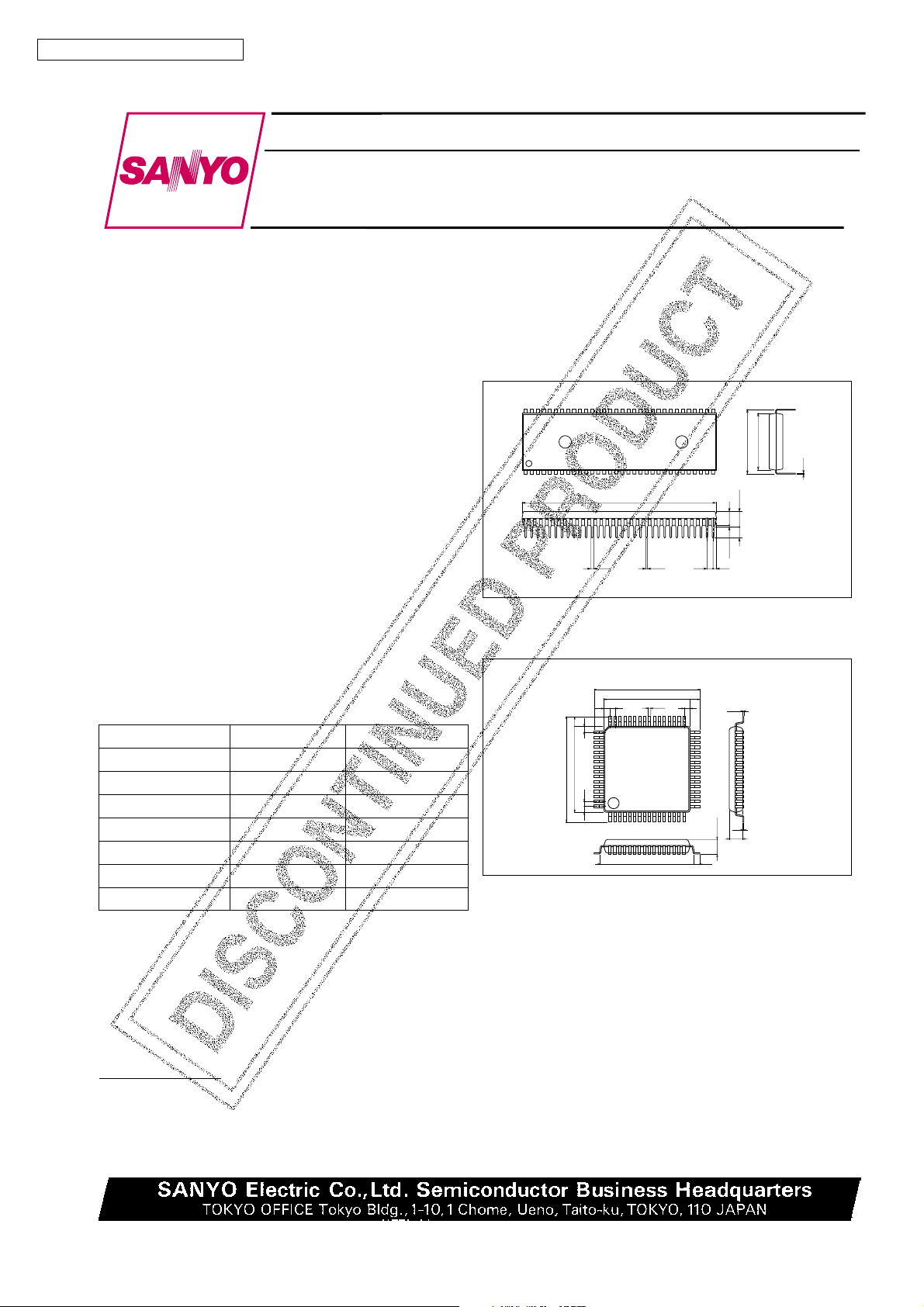
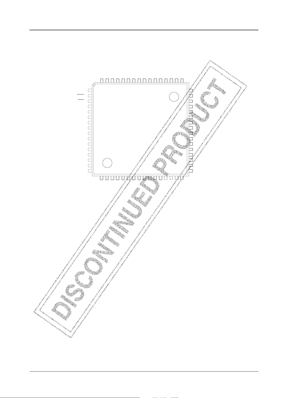
Package Dimensions
unit : mm
3071-DIP64S
[LC86P5032]
57.2
0.95 0.48 1.78 1.01
unit : mm
3159-QFP64E
[LC86P5032]
17.2
14.0
0.8
0.35
33
1
16
15.6
17.2
1.6
14.0
1.0
0.8
1.0
1.0
48
49
64
3364
19.5
321
5.0max
4.00.51min
3.2
SANYO : DIP52S
1.6
1.0
0.15
32
17
0.1
3.0max
2.7
0.8
SANYO : QFP64E
16.8
0.25
(4) Operating supply voltage : 4.5 to 6.0 V
(5) Instruction cycle time : 0.98 to 400 µs
(6) Operating temperature range : –30°C to +70°C
(7) Pins and package compatible with the mask ROM version
(8) Applicable mask version : LC865032/LC865028/LC865024/LC865020/LC865016/LC865012, LC865008
(9) Factory shipment : DIP-64S
QFP-64E
Programming service
We offer various services at nominal charges. These include ROM writing, ROM reading, and package stamping and screening.
Contact our local representatives for further information.
SANYO Electric Co., Ltd. Semiconductor LSI Div. Microcomputer Development Dep.
O3097HA (II)
No. 5631-1/22
Page 2
LC86P5032
Usage Notes
When using, please take note of the following.
(1) Differences between the LC86P5032 and the LC865000 series
Item LC86P5032 LC865032/28/24/20/16/12/08
Port status at reset Please refer to "Port status at reset" on the next page.
Operation after releasing reset The option is specified by degrees within 3 ms
after applying a 'H' level to the reset pin.
The program located at 00H is executed.
Operating voltage range 4.5 to 6.0 V 2.7 to 6.0 V
(V
)
DD
Total output current
[ ∑I
(1) ]
OAH
[ ∑I
(1) ]
OAH
Current drain Refer to 'Electrical Characteristics' on the semiconductor news.
[ I
(1)]
DDOP
[ I
(2)]
DDOP
[ I
(3)]
DDOP
[ I
(4)]
DDOP
• LC86P5032 Options
The program located at 00H is executed
immediately after applying a 'H' level to the
reset pin.
Option Pins, Circuits Option Settings
Configuration of input/output ports Port 0 1. Input : No pull-up MOS transistor
(Can be specified for Output : N-channel open drain
each bit.) 2. Input : Pull-up MOS transistor
Output : CMOS
Ports 1, 2 1. Input : No programmable pull-up MOS transistor
(Can be specified for Output : N-channel open drain
each bit.) 2. Input : Programmable pull-up MOS transistor
Output : CMOS
Ports 3, 4, 5 1. Input : No programmable pull-up MOS transistor
(Can be specified for Output : N-channel open drain
each bit.) 2. Input : Programmable pull-up MOS transistor
Output : CMOS
Port 7 pull-up MOS transistor Port 7 1. Pull-up MOS transistor not provided
(Can be specified for 2. Pull-up MOS transistor provided
each bit.) *P74 has no pull-up resistor option.
The port operation related to the option is different at reset. Please refer to the next table.
No. 5631-2/22
Page 3
LC86P5032
• Port configuration at reset
Pin Option settings LC86P5032 LC865032/28/24/20/16/12/08
P0 Input : No pull-up MOS transistor (Same as for the mask version) Input mode without pull-up MOS
Output : N-channel open drain transistor (Output is OFF)
Input : Pull-up MOS transistor Input mode Input mode with pull-up MOS
Output : CMOS • The Pull-up MOS transistor is not transistor (Output is OFF)
present during reset or several hundred
microseconds after releasing reset.
After that, the pull-up MOS transistor
is present. (Output is OFF)
P1,
Input : Programmable pull-up MOS transistor
P2 Output : N-channel open drain transistor (Output is OFF)
Input : Programmable pull-up MOS transistor
Output : CMOS transistor (Output is OFF)
P3, Input : Non-Programmable pull-up (Same as for the mask version) Input mode without pull-up MOS
P4, MOS transistor transistor (Output is OFF)
P5 Output : N-channel open drain
Input : Programmable pull-up MOS (Same as for the mask version) Input mode without pull-up MOS
transistor transistor (Output is OFF)
Output : CMOS
P7 Pull-up MOS transistor not provided (Same as for the mask version)
Pull-up MOS transistor provided Input mode Input mode with pull-up MOS
(Same as for the mask version) Input mode without pull-up MOS
(Same as for the mask version) Input mode without pull-up MOS
Input mode without pull-up MOS transistor
• The pull-up MOS transistor is not transistor
present during reset or several hundred
microseconds after releasing reset.
After that, the pull-up MOS transistor
is present.
(2) Option
The LC86P5032 uses 256 bytes addressed 7F00H to 7FFFH in program memory as option data area. This area does not affect the
execution of the program but means that the LC865032 program memory is 32512 bytes addressed 0000H to 7EFFH.
The option data is written using the option specifying program "SU865000. EXE". The option data is linked to the program area by
linkage loader "L865000. EXE".
(3) ROM space
7FFFH
7F00H
Option data
area 256 bytes
Option
Data Area
Option
Data Area
Option
Data Area
Option
Data Area
Option
Data Area
Option
Data Area
7EFFH
6FFFH
5FFFH
4FFFH
3FFFH
32K 28K 24K 20K 16K 12K 8K
0FFFH
LC865032 LC865028 LC865024 LC865020 LC865016 LC865012 LC865008
No. 5631-3/22
Page 4
LC86P5032
(4) Ordering information
1.When ordering identical mask ROM and PROM devices simultaneously.
Provide an EPROM containing the target memory contents together with separate order forms for each of the mask
ROM and PROM versions.
2.When ordering a PROM device.
Provide an EPROM containing the target memory contents together with an order form.
How to Use
(1) Specification of options
Programming data for the LC86P5032’s EPROM is required.
The debugged evaluation file (EVA file) must be converted to an INTEL-HEX formatted file (HEX file) with file converter
program EVA2HEX.EXE. The HEX file is used as the programming data for the LC86P5032.
(2) How to program the EPROM
The LC86P5032 can be programmed by an EPROM programmer with attachments W86EP5032D and W86EP5032Q.
• Recommended EPROM programmer
Supplier EPROM programmer
Advantest R4945, R4944, R4943
Andou AF-9704
AVAL PKW-1100, PKW-3000
Minato Electronics MODEL 1890A
• "27512 (Vp-p = 12.5 V) Intel high-speed programming" mode available. The address must be set to "0000H to 7FFFH"
and the jumper (DASEC) must be set 'OFF' at programming.
(3) How to use the data security function
"Data security" is a function to prevent EPROM data from being read.
Instructions on using the data security function:
1. Set the jumper of attachment 'ON'.
2. Attempt to program the EPROM. The EPROM programmer will display an error. The error indication is a result of
normal activity of the data security feature. This is not a problem with the EPROM programmer chip.
Notes
• The data security function is not carried out when the data of all addresses contain 'FF' at step 2 above.
• Data security cannot be executed when the sequential operation "BLANK=>PROGRAM=>VERIFY" is used at step 2 above.
• Set the jumper 'OFF' after execution of data security.
Pin 1 mark
OFF
O
OFF
Pin 1
ON
O
F
F
O
N
Data security OFF Data security OFF
Pin 1
N
OFF
ON
W86EP5032D W86EP5032Q
No. 5631-4/22
Page 5

Pin Assignment
LC86P5032
P10/SO0
P11/SI0/SB0
P12/SCK0
P13/SO1
P14/SI1/SB1
P15/SCK1
P16/BUZ
P17/PWM
TEST1
RES
XT1/P74
XT2
V
VSS
SS
CF1
CF2
V
DD
VDD
P80/AN0
P81/AN1
P82/AN2
P83/AN3
P84/AN4
P85/AN5
P86/AN6
P87/AN7
P70/INT0
P71/INT1
P72/INT2/T0IN
P73/INT3/T0IN
P30
P31
P32
P33
10
11
12
13
14
15
16
17
18
19
20
21
22
23
24
25
26
27
28
29
30
31
32
1
2
3
4
5
6
7
8
9
64
63
62
61
60
59
58
57
56
55
54
53
52
51
50
49
48
47
46
45
44
43
42
41
40
39
38
37
36
35
34
33
P07
P06
P05
P04
P03
P02
P01
P00
P27
P26
P25
P24
P23
P22
P21
P20
VDDV
PP
VDDVPP
V
SS
VSS
P51
P50
P47
P46
P45
P44
P43
P42
P41
P40
P37
P36
P35
P34
Top view
SANYO : DIP64S
No. 5631-5/22
Page 6
0
Pin Assignment
LC86P5032
TEST1
RES
XT1/P74
XT2
V
SS
VSS
CF1
CF2
V
DD
VDD
P80/AN0
P81/AN1
P82/AN2
P83/AN3
P84/AN4
P85/AN5
P86/AN6
P87/AN7
64
48
49
50
51
52
53
54
55
56
57
58
59
60
61
62
63
P16/BUZ
P15/SCK1
P17/PWM
47
46
123
P70/INT0
P71/INT1
P72/INT2/T0IN
P13/SO1
P11/SI0/SB
P12/SCK0
P14/SI1/SB1
43
P31
41
42
789
P32
44
45
456
P30
P73/INT3/T0IN
P10/SO0
P06
P07
40
39
P34
P35
P33
P05
P04
37
38
101112
P36
P03
36
131415
P40
P37
P02
35
P41
P01
34
P42
31
30
29
28
27
26
25
24
23
22
21
20
19
18
17
P00
33
P43
32
16
P27
P26
P25
P24
P23
P22
P21
P20
VDDV
PP
VDDVPP
VSS
V
SS
P51
P50
P47
P46
P45
P44
Top view
SANYO : QFP64E
No. 5631-6/22
Page 7
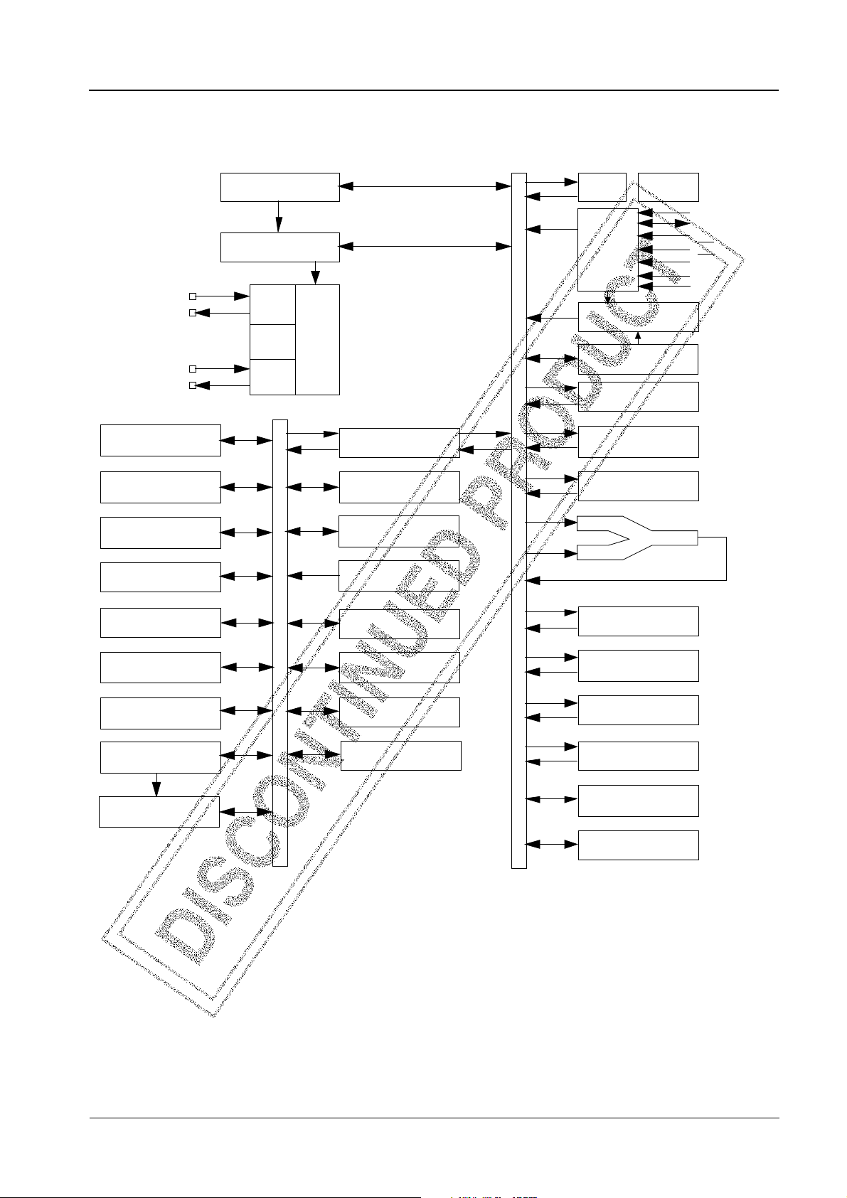
System Block Diagram
LC86P5032
Base timer
SIO 0
SIO 1
Timer 0
Interrupt control
Standby control
CF
RC
X tal
Colck
generator
Bus interface
Port 1
Port 7
Port 8
IR PLA
PROM
control
PROM(32KB)
PC
ACC
B register
C register
ALU
A16 to A0
D7 to D0
TA
CE
OE
DASEC
DD VPP
V
Timer 1
ADC
INT0 to INT3
Noise rejection filter
Real-time
service
XRAM
128 bytes
Port 2
Port 3
Port 4
Port 5
PSW
RAR
RAM
Stack
pointer
Port 0
Watchdog timer
No. 5631-7/22
Page 8

LC86P5032
LC86P5032 Pin Description
Pin name I/O Function description Option Function in PROM mode
V
SS
V
DD
VDDV
PP
PORT0 I/O • 8-bit input/output port • Pull-up resistor :
P00 to P07 • Input for port 0 interrupt Present/Not present
PORT1 I/O • 8-bit input/output port Output form : CMOS/ Data input/output
P10 to P17 • Data direction can be specified for each bit. N-channel open drain • D0 to D7
PORT2 I/O • 8-bit input/output port Output form : CMOS/
P20 to P27 • Data direction can be specified for each bit. N-channel open drain
PORT3 I/O • 8-bit input/output port Output form : CMOS/ Address input
P30 to P37 • Data direction can be specified for each bit. N-channel open drain • A7 to A0
PORT4 I/O • 8-bit input/output port Output form : CMOS/ Address input
P40 to P47 • Data direction can be specified for each bit. N-channel open drain • A14 to A8 (*5)
PORT5 I/O • 2-bit input/output port. Output form : CMOS/
P50 to P51 • Data direction can be specified for each bit. N-channel open drain
PORT7 • 5-bit input port Pullup resistor :
P70 I/O P70 : INT0 input/HOLD release/N-channel (P70, 71, 72, 73) Input of PROM control signal
P71 to P74 I P71 : INT 1 input/HOLD release. resistor. • OE (*2)
Power supply pin(–)
Power supply pin(+)
Power supply pin(+) Power for programming
• Input/output in nibble units
• Input for HOLD release • Output form : CMOS/
N-channel open drain.
• Other pin functions
P10 : SIO0 data output
P11 : SIO0 data input/bus input/output
P12 : SIO0 clock input/output
P13 : SIO1 data output
P14 : SIO1 data input/ bus input/output
P15 : SIO1 clock input/output
P16 : Buzzer output
P17 : Timer 1 output (PWM output)
• 15 V withstand at N-ch open-drain output
• 15 V withstand at N-ch open-drain output • P47 : TA (*4)
• 15 V withstand at N-ch open-drain output
• Other pin functions Present/Not present
Tr. output for watchdog timer. * P74 has no pull-up • DASEC (*1)
P72 : INT 2 input/timer 0 event input. • CE (*3)
P73 : INT 3 input with noise filter/timer 0
event input.
P74 : Input pin XT1 for 32.768 kHz crystal
oscillation
• Interrupt received format, vector address.
Rising Falling Rising High Low Vector
& level level
falling
INT0 Enable Enable Disable Enable Enable 03H
INT1 Enable Enable Disable Enable Enable 0BH
INT2 Enable Enable Enable Disable Disable 13H
INT3 Enable Enable Enable Disable Disable 1BH
No. 5631-8/22
Page 9

LC86P5032
Pin name I/O Function description Option Function in PROM mode
PORT8 I • 8-bit input port
P80 to P87 • Other functions
AD input port (8 port pins)
RES I Reset pin
TEST1 O Test pin
Should be left open.
XT1/P74 I • Input pin for 32.768 kHz crystal oscillation
• Other function : Input port P74
When not used, connect to V
XT2 O Output pin for 32.768 kHz crystal oscillation
When not used, should be left open.
CF1 I Input pin for ceramic resonator oscillation
CF2 O Output pin for ceramic resonator oscillation
• All port options can be specified in bit units.
*1 Memory select input for data security
*2 Output enable input
*3 Chip enable input
*4 TA ➝ PROM control signal input
*5 A14 ➝ Address input
DD
.
• Connect as shown in the following figure to reduce noise into V
Short-circuit the V
Short-circuit the V
pin to the VDDVPP pin.
DD
pin to the VSS pin.
SS
Power
supply
DD
pin.
V
DD
VDDV
V
SS
PP
LSI
V
SS
No. 5631-9/22
Page 10

LC86P5032
1. Absolute Maximum Ratings at Ta = 25°C, VSS = 0 V
Parameter Symbol Pins Conditions Ratings Unit
VDD[V] min typ max
Supply voltage VDD max VDD, VDDV
PP
Input voltage VI(1) • Ports 71, 72, 73, 74 –0.3 VDD+0.3
• Port 8
• RES
Input/output VIO(1) • Ports 0, 1, 2 –0.3 VDD+0.3
voltage • Ports 3, 4, 5 of
CMOS output
Highlevel
output
current
Peak
output
current
Total
VIO(2) •
I
(1) Ports 0, 1, 2, 3, 4, 5 • CMOS output –4mA
OPH
∑I
(1) Ports 0, 1, 2 Total of all pins –25
OAH
Ports 3, 4, 5 of opendrain output
output
Lowlevel
output
current
current
Peak
output
current
Total
output
current
∑I
(2) Ports 3, 4, 5 Total of all pins –20
OAH
I
(1) Ports 0, 1, 2, 3, 4, 5 At each pin 20
OPL
I
(2) Port 70 At each pin 15
OPL
∑I
(1) Ports 0, 1, 70 Total of all pins 40
OAL
∑I
(2) Port 2 Total of all pins 40
OAL
∑I
(3) Ports 3, 4, 5 Total of all pins 80
OAL
Power dissipation Pd max(1) DIP64S Ta = –30°C+70°C 720 mW
(max.)
Pd max(2) QFP64E Ta = –30°C+70°C 420
Operating Topr –30 70 °C
temperature range
Storage Tstg –65 150
temperature range
VDD = VDDV
• At each pin
PP
–0.3 +7.0 V
–0.3 15
No. 5631-10/22
Page 11

LC86P5032
2. Recommended Operating Range at Ta = –30°C to +70°C, VSS = 0 V
Parameter Symbol Pins Conditions Ratings Unit
VDD[V] min typ max
Operating voltage VDD(1) V
DD
range tCYC ≤ 400 µs
HOLD voltage V
HD
V
DD
Input high VIH(1) Port 0 (Schmitt) Output disabled 4.5 to 6.0 0.4V
voltage +0.9
VIH(2) • Ports 1, 2 Output disabled 4.5 to 6.0 0.75V
• Ports 72, 73
(Schmitt)
VIH(3) • Port 70 Output N-channel 4.5 to 6.0 0.75V
Port input/interrupt. transistor OFF
• Port 71
• RES (Schmitt)
VIH(4) Port 70 Output N-channel 4.5 to 6.0 0.9V
Watchdog timer transistor OFF
VIH(5) • Port 74 Output N-channel 4.5 to 6.0 0.75V
• Port 8 transistor OFF
VIH(6) Ports 3, 4, 5 of Output disabled 4.5 to 6.0 0.75V
CMOS output
(Schmitt)
VIH(7) Ports 3, 4, 5 of open Output disabled 4.5 to 6.0 0.75V
drain output
(Schmitt)
Input low VIL(1) Port 0 (Schmitt) Output disabled 4.5 to 6.0 V
voltage
V
(2) • Ports 1, 2, 3, 4, 5 Output disabled 4.5 to 6.0 V
IL
• Ports 72,73
(Schmitt)
VIL(3) • Port 70 N-channel transistor 4.5 to 6.0 V
Port input/interrupt. OFF
• Port 71
• RES (Schmitt)
VIL(4) Port 70 N-channel transistor 4.5 to 6.0 V
Watchdog timer OFF –1.0
VIL(5) • Port 74 N-channel transistor 4.5 to 6.0 V
• Port 8 OFF
Operation cycle tCYC 4.5 to 6.0 0.98 400 µs
time
0.98 µs ≤ tCYC 4.5 6.0 V
RAM and registers 2.0 6.0
retain their pre-HOLD
mode values.
V
13.5
0.2V
0.25V
0.25V
0.8V
0.25V
V
DD
DD
V
DD
V
DD
V
DD
V
DD
DD
DD
DD
DD
DD
DD
DD
DD
DD
DD
DD
DD
SS
SS
SS
SS
SS
No. 5631-11/22
Page 12

LC86P5032
Parameter Symbol Pins Conditions Ratings Unit
VDD[V] min typ max
Oscillation FmCF(1) CF1, CF2 • 12 MHz (ceramic 4.5 to 6.0 11.76 12 12.24 MHz
frequency range resonator oscillation).
(Note 1) • Refer to Figure 1.
FmCF(2) CF1, CF2 • 3 MHz (ceramic 4.5 to 6.0 2.94 3 3.06
resonator oscillation).
• Refer to Figure 1.
FmRC RC oscillation 4.5 to 6.0 0.4 0.8 2.0
FsXtal XT1, XT2 • 32.768 kHz (crystal 4.5 to 6.0 32.768 kHz
oscillation).
• Refer to Figure 2.
Oscillation stable tmsCF(1) CF1, CF2 • 12 MHz (ceramic 4.5 to 6.0 0.03 0.5 ms
time period resonator oscillation).
(Note 1) • Refer to Figure 3.
tmsCF(2) CF1, CF2 • 3 MHz (ceramic 4.5 to 6.0 0.2 2
resonator oscillation).
• Refer to Figure 3.
tssXtal XT1, XT2 • 32.768 kHz (crystal 4.5 to 6.0 1 1.5 s
oscillation).
• Refer to Figure 3.
(Note 1) The oscillation constants are shown on Table 1 and Table 2.
No. 5631-12/22
Page 13

LC86P5032
3. Electrical Characteristics at Ta= –30°C to +70°C , VSS = 0 V
Parameter Symbol Pins Conditions Ratings Unit
VDD [V] min typ max
Input high
current
Input low
current
Output high
voltage
Output low
voltage
Pull-up MOS
transistor resistance
Hysteresis
voltage
Pin capacitance
IIH(1) 4.5 to 6.0 5 µA
•Ports 3, 4, 5 at
open-drain output
IIH(2) 4.5 to 6.0 1
•Port 0 without
pull-up MOS
transistor
•Ports 1, 2, 3, 4, 5
IIH(3) 4.5 to 6.0 1
•Ports 70, 71, 72, 73
without pull-up
MOS transistor
•Port 8
IIH(4) 4.5 to 6.0 1
IIL(1) 4.5 to 6.0 –1
•RES
•Ports 1, 2, 3, 4, 5
•Port 0 without
pull-up MOS
transistor
IIL(2) 4.5 to 6.0 –1
•Ports 70, 71, 72, 73
without pull-up
MOS transistor
•Port 8
IIL(3) 4.5 to 6.0 –1
VOH(1) 4.5 to 6.0 VDD–1V
•RES
•Ports 0, 1, 2, 3, 4, 5
at CMOS output
VOH(2) 4.5 to 6.0 VDD–0.5
VOL(1) 4.5 to 6.0 1.5
Ports 0, 1, 2, 3, 4, 5
VOL(2) 4.5 to 6.0 0.4
VOL(3) 4.5 to 6.0 0.4
Port 70
VOL(4) 4.5 to 6.0 0.4
Rpu 4.5 to 6.0 15 40 70 kΩ
•Ports 0, 1, 2, 3, 4, 5
•Ports 70, 71, 72, 73
V
HIS
•Ports 0, 1, 2, 3, 4, 5
•Ports 70, 71, 72, 73
•RES
CP 4.5 to 6.0 10 pF
All pins
•Output disabled
= 13.5 V
•V
IN
(including off-state leak
current of output transistor)
•Output disabled
•Pull-up MOS transistor
OFF. VIN = V
DD
(including off-state leak
current of output transistor)
VIN = V
DD
VIN = V
DD
•Output disabled
•Pull-up MOS transistor
OFF. V
IN
= V
SS
(including off-state leak
current of output transistor)
VIN = V
SS
VIN = V
SS
IOH = –1.0 mA
I
= –0.1 mA
OH
I
= 10 mA
OL
I
= 1.6 mA
OL
I
= 1 mA
OL
IOL = 0.5 mA
V
= 0.9 V
OH
DD
Output disable
•f = 1 MHz
•Unmeasured input
pins are set to
V
level.
SS
•Ta = 25°C
4.5 to 6.0 0.1V
DD
V
No. 5631-13/22
Page 14

LC86P5032
4. Serial Input/Output Characteristics at Ta = –30°C to +70°C , VSS = 0 V
Parameter Symbol Pins Conditions Ratings Unit
VDD [V] min typ max
Cycle
Low-
level
pulse
width
Input clock
Highlevel
pulse
width
Cycle
Serial clock
Lowlevel
pulse
width
Output clock
Highlevel
pulse
width
Data setup
time
Data hold
time
Serial input
Output delay
time
(Serial clock
is extrnal
clock.)
tCKCY(1) SCK0, SCK1 4.5 to 6.0 2 tCYC
tCKL(1) 4.5 to 6.0 1
tCKH(1) 4.5 to 6.0 1
tCKCY(2) SCK0, SCK1 4.5 to 6.0 2
tCKL(2) 4.5 to 6.0 1/2tCKYC
tCKH(2) 4.5 to 6.0 1/2tCKYC
tICK • SI0, SI1 4.5 to 6.0 0.1 µs
• SB0, SB1
tCKI 4.5 to 6.0 0.1
tCKO(1) • SO0, SO1 4.5 to 6.0 7/12tCYC
• SB0, SB1 +0.2
Refer to Figure 5.
• Use pullup resistor
(1 kΩ) when set to
open-drain output.
• Refer to Figure 5.
• Data set-up to
SCK0, 1
• Data hold from
SCK0, 1
• Refer to Figure 5.
• Use a pullup resistor
(1 kΩ) when set to
open-drain output.
Output delay
Serial output
time
(Serial clock
is internal
clock.)
tCKO(2) 4.5 to 6.0 1/3tCYC
• Data hold from
SCK0, 1
• Refer to Figure 5.
+0.2
No. 5631-14/22
Page 15

LC86P5032
5. Pulse Input Conditions at Ta = –30°C to +70°C, VSS = 0 V
Parameter Symbol Pins Conditions Ratings Unit
VDD [V] min typ max
High/low-level tPIH(1) • INT0, INT1 4.5 to 6.0 1 tCYC
pulse width tPIL(1) • INT2/T0IN
• INT3
tPIH(2) INT3 4.5 to 6.0 2
tPIL(2) (The noise rejection
clock selected to 1/1.)
tPIH(3) INT3 4.5 to 6.0 32
tPIL(3) (The noise rejection
clock selected to
1/16.)
tPIL(4) RES 4.5 to 6.0 200 µs
6. A/D Converter Characteristics at Ta = –30°C to +70°C, VSS = 0 V
Parameter Symbol Pins Conditions Ratings Unit
Resolution
Absolute
precision (Note 2)
Conversion
time
Analog input
voltage range
Analog port
input current
N 8 bit
ET 4.5 to 6.0 ±1/5 LSB
tCAD 4.5 to 6.0 15.68 65.28 µs
V
I
AINH
I
AINL
AIN
AN0 to AN7
• Interrupt acceptable
• Timer 0 pulse
countable
• Interrupt acceptable
• Timer 0 pulse
countable
• Interrupt acceptable
• Timer 0 pulse
countable
Reset acceptable
A/D conversion
time = 16 × tCYC
(ADCR2 = 0)
(Note 3)
A/D conversion
time = 32 × tCYC
(ADCR2 = 1)
(Note 3)
= V
V
AIN
DD
V
= V
AIN
SS
VDD [V] min typ max
(tCYC = (tCYC =
0.98 µs) 4.08 µs)
31.36 130.56
(tCYC = (tCYC =
0.98 µs) 4.08 µs)
4.5 to 5.5 V
SS
V
DD
4.5 to 5.5 +1 µA
4.5 to 5.5 –1
V
(Note 2) Quantizing error (±1/2 LSB) is ignored.
(Note 3) The conversion time is the period from execution of the instruction to start conversion to the completion of shifting the
A/D converted value to the register.
No. 5631-15/22
Page 16

LC86P5032
7. Current Drain Characteristics at Ta = –30°C to +70°C , VSS = 0 V
Parameter Symbol Pins Conditions Ratings Unit
VDD [V] min typ max
Current drain
during basic
operation
(Note 4)
I
DDOP
(1) V
DD
• FmCF = 12 MHz for
4.5 to 6.0 13 26 mA
ceramic resonator
oscillation.
• FsXtal = 32.768 kHz for
crystal oscillator.
• System clock :
CF oscillator.
• Internal RC oscillator
stopped.
I
(2) 4.5 to 6.0 7 14
DDOP
• FmCF = 3 MHz for
ceramic resonator
oscillation.
• FsXtal = 32.768 kHz for
crystal oscillator.
• System clock :
CF oscillator.
• Internal RC oscillator
stopped.
I
(3) 4.5 to 6.0 4 10
DDOP
• FmCF = 0 Hz
(when oscillator stops).
• FsXtal = 32.768 kHz for
crystal oscillator.
• System clock :
RC oscillator.
I
(4) 4.5 to 6.0 4 8
DDOP
• FmCF = 0 Hz
(when oscillator stops).
• FsXtal = 32.768 kHz for
crystal oscillator.
• System clock :
crystal oscillator.
• Internal RC oscillator
stopped.
No. 5631-16/22
Page 17

LC86P5032
Parameter Symbol Pins Conditions Ratings Unit
VDD [V] min typ max
Current drain at
HALT mode
(Note 4)
Current drain at
HOLD mode
(Note 4)
I
DDHALT
(1) V
DD
• HALT mode
4.5 to 6.0 5 10 mA
• FmCF = 12 MHz for
ceramic resonator
oscillation.
• FsXtal = 32.768 kHz for
crystal oscillator.
• System clock :
CF oscillator.
• Internal RC oscillator
stopped.
I
(2) 4.5 to 6.0 2.2 4.6
DDHALT
• HALT mode
• FmCF = 3 MHz for
ceramic resonator
oscillation.
• FsXtal = 32.768 kHz for
crystal oscillator.
• System clock :
CF oscillator.
• Internal RC oscillator
stopped.
I
(3) 4.5 to 6.0 550 1100 µA
DDHALT
• HALT mode
• FmCF = 0 Hz
(when oscillator stops).
• FsXtal = 32.768 kHz for
crystal oscillator.
• System clock :
RC oscillator
I
(4) 4.5 to 6.0 25 100
DDHALT
• HALT mode
• FmCF = 0 Hz
(when oscillator stops).
• FsXtal = 32.768 kHz for
crystal oscillator.
• System clock :
crystal oscillator.
• Internal RC oscillator
stopped.
I
(1) V
DDHOLD
I
(2) 2.5 to 4.5 0.02 20
DDHOLD
DD
HOLD mode
4.5 to 6.0 0.05 30
(Note 4) The currents of output transistors and pull-up transistors are ignored.
No. 5631-17/22
Page 18

LC86P5032
Table 1. Ceramic Resonator Oscillation Guaranteed Constants (Main clock)
Oscillation type Supplier Oscillator C1 C2
12 MHz ceramic resonator Murata CSA12.0MTZ 33 pF 33 pF
oscillation CST12.0MTW on chip
Kyocera KBR-12.0M 33 pF 33 pF
3 MHz ceramic resonator Murata CSA3.00MG040 100 pF 100 pF
oscillation CST3.00MGW040 on chip
Kyocera KBR-3.0MS 47 pF 47 pF
• For both C1 and C2, the K rank (±10%) and SL characteristics must be used.
Table 2. Crystal Oscillaion Guaranteed Constants (Sub-clock)
Oscillation type Supplier Oscillator C3 C4
32.768 kHz crystal oscillation Kyocera KF-38G-13P0200 18 pF 18 pF
• For both C3 and C4, the J rank (±5%) and CH characteristics must be used.
(If high precision is not necessary, use K rank (±10%) and SL characteristics.)
Notes • Since the circuit pattern affects the oscillation frequency, place the oscillation-related parts as close to the oscillation pins
as possible with the shortest possible pattern length.
• If you use other oscillators herein, we provide no guarantee for the characteristics.
CF1
C1
Figure 1 Ceramic Resonator Oscillation Figure 2 Crystal Oscillation
CF
Main-clock circuit Sub-clock circuit
CF2
C2
XT1
C3 C4
X tal
XT2
No. 5631-18/22
Page 19

Power supply
LC86P5032
V
DD
VDD lower limit
0V
RES
Internal RC
resonator
oscillation
CF1, CF2
XT1, XT2
Operation mode
HOLD release signal
Internal RC
resonator
oscillation
CF1, CF2
Reset time
t
msCF
t
ssXtal
Unfixed
Reset
Instruction execution mode
<Reset time and oscillation stable time.>
Valid
t
msCF
XT1, XT2
Operation mode
RES
t
ssXtal
HOLD
Instruction execution mode
<HOLD release signal and oscillation stable time.>
Figure 3 Oscillation Stable Time
VDD
V
DD
R
RES
R
RES
C
C
RES
RES
The values of C
such that reset time is at least 200 µs, measured from
(Note) Fix the value of C
the moment the power exceeds the V
is sure to reset untill 200µs, after
RES
and R
Power supply has been over inferior
limit of supply voltage.
should be determined
RES
RES
, R
lower limit.
DD
RES
that
Figure 4 Reset Circuit
No. 5631-19/22
Page 20

LC86P5032
0.5VDD
0.5 V
< AC timing point >
DD
SCK0
SCK1
SI0
SI1
SO0,SO1
SB0,SB1
t
CKCY
t
CKL
t
t
ICK
t
CKO
< Timing >
Figure 5 Serial Input/Output Test Conditions
CKI
t
CKH
VDD
1kΩ
50pF
< Test load >
t
PIL
Figure 6 Pulse Input Timing Conditions
t
PIH
No. 5631-20/22
Page 21

LC86P5032
Usage Notes
• The construction of the one-time programmable microcontroller with a blank built-in PROM makes it impossible for Sanyo
to completely factory-test it before shipping. To prove reliability of the programmed devices, the screening procedure
shown in the following figure should always be followed.
• It is not possible to perform a writing test on the blank PROM. 100% yield, therefore, cannot be guaranteed.
• Ensure dry packaging
The environment must be held at a temparature of 30°C or less and a humidity level of 70% or less.
• After opening the packing
The preparation procedures shown in the following figure should always be followed prior to mounting the packages on the
substrate. After opening the packing, a controlled environment must be maintained until soldering.
The environment must be held at a temperature of 30°C or less and a humidity level of 70% or less. Please solder within 96
hours.
a. Shipping with a blank PROM (Data to be programmed by customer)
DIP
Programming and
verifying
Recommended process of screening
Heat-soak
150 ± 5°C, 24 Hr
+1
–0
Program reading test
Mounting
QFP
Programming and
verifying
Recommended process of screening
Heat-soak
150 ± 5°C, 24 Hr
+1
–0
Program reading test
Mounting
b. Shipping with programmed PROM (Data programmed by Sanyo)
Mounting
QFPDIP
Mounting
No. 5631-21/22
Page 22

LC86P5032
Any and all SANYO products described or contained herein do not have specifications that can handle
applications that require extremely high levels of reliability, such as life-support systems, aircraft’s
control systems, or other applications whose failure can be reasonably expected to result in serious
physical and/or material damage. Consult with your SANYO representative nearest you before using
any SANYO products described or contained herein in such applications.
SANYO assumes no responsibility for equipment failures that result from using products at values that
exceed, even momentarily, rated values (such as maximum ratings, operating condition ranges, or other
parameters) listed in products specifications of any and all SANYO products described or contained
herein.
Specifications of any and all SANYO products described or contained herein stipulate the performance,
characteristics, and functions of the described products in the independent state, and are not guarantees
of the performance, characteristics, and functions of the described products as mounted in the customer’s
products or equipment. To verify symptoms and states that cannot be evaluated in an independent device,
the customer should always evaluate and test devices mounted in the customer’s products or equipment.
SANYO Electric Co., Ltd. strives to supply high-quality high-reliability products. However, any and all
semiconductor products fail with some probability. It is possible that these probabilistic failures could
give rise to accidents or events that could endanger human lives, that could give rise to smoke or fire,
or that could cause damage to other property. When designing equipment, adopt safety measures so
that these kinds of accidents or events cannot occur. Such measures include but are not limited to protective
circuits and error prevention circuits for safe design, redundant design, and structural design.
In the event that any or all SANYO products(including technical data,services) described or
contained herein are controlled under any of applicable local export control laws and regulations,
such products must not be exported without obtaining the export license from the authorities
concerned in accordance with the above law.
No part of this publication may be reproduced or transmitted in any form or by any means, electronic or
mechanical, including photocopying and recording, or any information storage or retrieval system,
or otherwise, without the prior written permission of SANYO Electric Co. , Ltd.
Any and all information described or contained herein are subject to change without notice due to
product/technology improvement, etc. When designing equipment, refer to the “Delivery Specification”
for the SANYO product that you intend to use.
Information (including circuit diagrams and circuit parameters) herein is for example only ; it is not
guaranteed for volume production. SANYO believes information herein is accurate and reliable, but
no guarantees are made or implied regarding its use or any infringements of intellectual property rights
or other rights of third parties.
This catalog provides information as of October, 1997. Specifications and information herein are subject to change without notice.
No. 5631-22/22
 Loading...