

SANYO LC86E7148 Datasheet
Ordering number : ENN*6748
CMOS IC
LC86E7148
8-Bit Single Chip Microcontroller
with the UVEPROM
Preliminary
Overview
The LC86E7148 is a CMOS 8-bit single chip microcontroller with UVEPROM for the LC867100 series. This
microcontroller has the function and the pin description of the LC867100 series mask ROM version, and 48K-byte EPROM.
The program data is rewritable. It is suitable to develop the program.
Features
(1) Option switching by EPROM data
The option function of the LC867100 series can be specified by the EPROM data.
LC86E7148 can be checked the functions of the trial pieces using the mass production board.
(2) Internal EPROM capacity : 49152 bytes
(3) Internal RAM capacity : 1152 bytes
Used EPROM or RAM capacity are equal ROM or RAM capacity of mask ROM version which applies LC86E7148.
Mask ROM version EPROM capacity RAM capacity
LC867148 49152 bytes 1152 bytes
LC867140 40960 bytes 1152 bytes
LC867132 32768 bytes 768 bytes
LC867128 28672 bytes 768 bytes
LC867124 24576 bytes 768 bytes
LC867120 20480 bytes 640 bytes
LC867116 16384 bytes 640 bytes
LC867112 12288 bytes 512 bytes
LC867108 8192 bytes 512 bytes
(4) Operating supply voltage : 4.5V to 6.0V
(5) Instruction cycle time : 1µs to 366µs
(6) Operating temperature : +10°C to +40°C
(7) The pin compatible with the LC867100 series mask ROM devices
(8) Applicable mask ROM version : LC867148/LC867140/LC867132/LC8671 28/LC867124/LC867120
/LC867116/LC867112/LC867108
(9) Factory shipment : QIC80S
Ver.1.01A
D1694
91400 RM (IM) HK No.6748-1/20

LC86E7148
Notice for use
At using, take notice of the followings.
(1) A point of difference LC86E7148 and LC867100 series
Item LC86E7148 LC867148/40/32/28/24/20/16/12/08
Port form at reset Please refer ‘Port form at reset’ on next page.
Operation after reset
releasing
Operating supply
voltage range (VDD)
Total output current
[∑IOAL(2)]
[∑IOAL(3)]
Power dessipation
LC86E7148 uses 256 bytes that is addressed on 0FF00H to FFFFH in the program memory as the option configuration data
area. This option configuration can execute all options which LC867100 series have. Next tables show the options that
correspond and not correspond to LC86E7148.
• A kind of the option corresponding of the LC86E7148
A kind of option Pins, Circuits Contents of the option
Input/output form of
input/output ports
Pull-up MOS Tr. of
input port
*1) Specified in a bit.
*2) Specified in nibble unit. Pull-up MOS Tr. is not provided in N-channel open drain output port.
The port operation related the option is different at reset. Refer to the next table.
The option is specified until 3ms after
going to a ‘H’ level to the reset terminal
by degrees. The program is executed from
00H of the program counter.
4.5V to 6.0V 2.5V to 6.0V
Refer to ‘electrical characteristics’ on the semiconductor news.
Port 0
(specified in a bit)
Port 1
(specified in a bit)
*1
Port 7
(specified in a bit) *1
Each of P74 and P75 has no
option
1. Input : No Pull-up MOS Tr.
Output : N-channel open drain *1
2. Input : Pull-up MOS Tr.
Output : CMOS *2
1. Input : Programmable pull-up MOS Tr.
Output : N-channel open drain
2. Input : Programmable pull-up MOS Tr.
Output : CMOS
1. No Pull-up MOS Tr.
2. Pull-up MOS Tr.
The program is executed from 00H of the
program counter immediately after going
to a ‘H’ level to the reset terminal.
No.6748-2/20
LC86E7148
(2) Option
The option data is created by the option specified program “SU86K.EXE”. The created option data is linked to the
program area by linkage loader “L86K.EXE”.
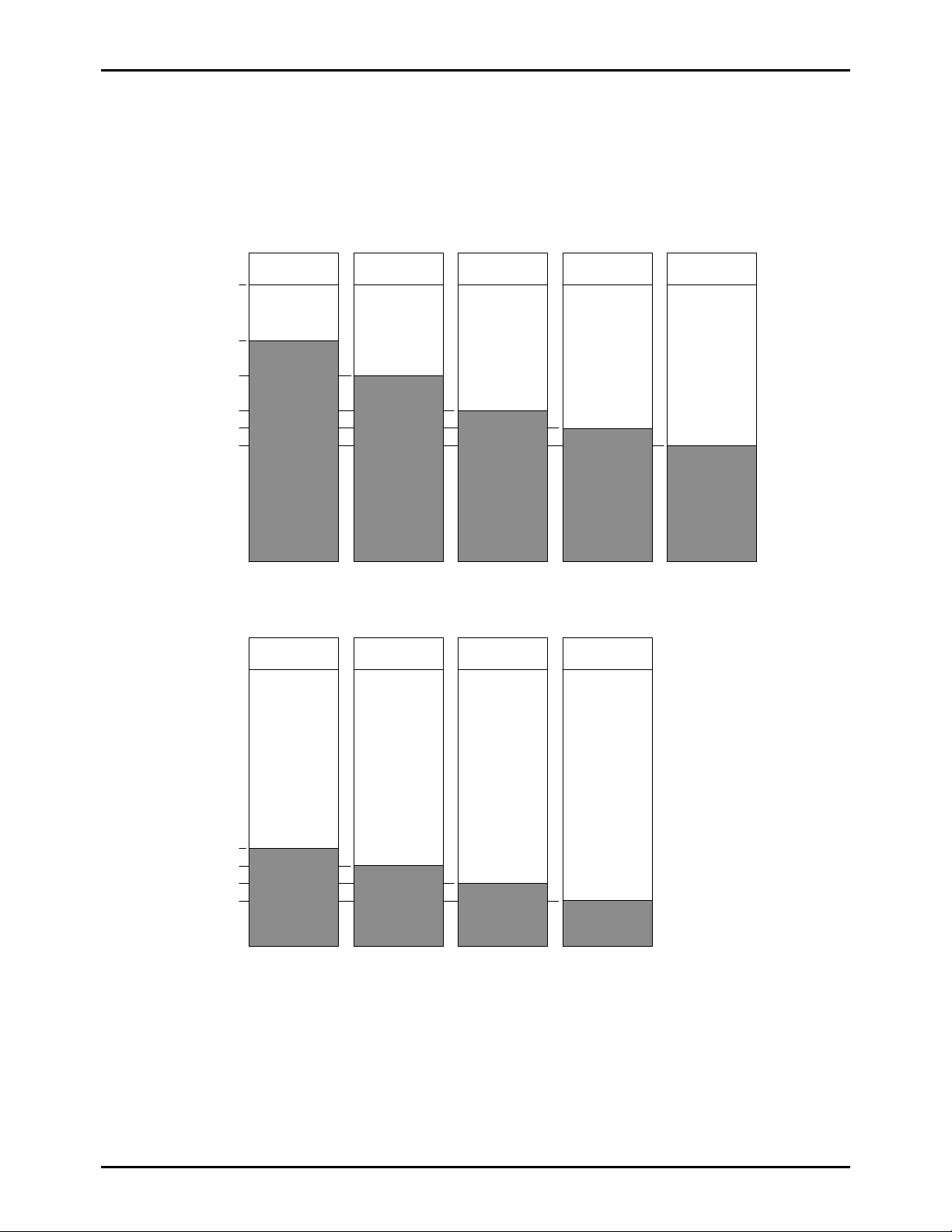
(3) ROM space
LC86E7148 and LC867100 series use 256 bytes that is addressed on 0FF00H to 0FFFFH in the program memory as the
option specified data area. These program memory capacity are 49152 bytes that is addressed on 0000H to 0BFFFH.
0FFFFH
0FF00H
0EFFFH
0DFFFH
0CFFFH
0BFFFH
0AFFFH
9FFFH
8FFFH
7FFFH
6FFFH
5FFFH
4FFFH
3FFFH
2FFFH
1FFFH
0FFFH
0000H
0FFFFH
0FF00H
0EFFFH
0DFFFH
0CFFFH
0BFFFH
0AFFFH
9FFFH
8FFFH
7FFFH
6FFFH
5FFFH
4FFFH
3FFFH
2FFFH
1FFFH
0FFFH
0000H
Option data
area 256 bytes
Program area
48K bytes
LC867148 LC867140
Option data
area 256 bytes
Program area
20K bytes
LC867120 LC867116
Option
Data Area
Program area
40K bytes
Option
Data Area
Program area
16K bytes
Option
Data Area
Program area
32K bytes
LC867132
Option
Data Area
Program area
12K bytes
LC867112
Option
Data Area
Program area
28K bytes
LC867128
Option
Data Area
Program area
8K bytes
LC867108
Option
Data Area
Program area
24K bytes
LC867124
No.6748-3/20

LC86E7148
How to use
(1) Specification of option
The LC86E7148 must be programmed after specifying option data. The option is specified by “SU86K.EXE”. The
specified option file and the file created by our macro assembler “M86K.EXE” are linked by our linkage loader
“L86K.EXE” which creates .HE X file, then the option code is put i n the option specified area ( 0FF00H to 0FFFFH) of
its .HEX file.
(2) How to program for the EPROM
The LC86E7148 can be programmed by EPROM programmer with attachment ; W86EP7148Q
• Recommended EPROM programmer
Productor EPROM programmer
Advantest R4945, R4944, R4943
Andou AF-9704
AVAL PKW-1100, PKW-3000
Minato electronics MODEL1890A
• “27512 (Vpp=12.5V) Intel high speed programming” mode available. T he address must be set to “0 to 0FFFFH” and a
jumper (DASEC) must be set to ‘OFF’ at programming.
(3) How to use the data security function
“Data security” is the disabled function to read the data of the EPROM.
The following is the process in order to execute the data security.
1. Set ‘ON’ the jumper of attachment.
2. Program again. Then EPROM programmer displays the error. The error means normally activity of the data
security. It is not a trouble of the EPROM programmer or the LSI.
Notes
• Data security is not executed when the data of all address have ‘FFH’ at the sequence 2 above.
• The programming by a sequential operation “BLANK=>PROGRAM=>VERIFY” cannot be executed data security at the
sequence 2 above.
• Set to ‘OFF’ the jumper after executing the d ata security.
(4) How to eliminate
The programming data can be erased by using the EPROM eraser.
(5) Shielding
The UVEPROM (ultraviolet erasable programmable ROM) is in it. Put the seal on the window in use.
Data security
Not data security
W86EP7148Q
No.6748-4/20

Pin Assignment
COM1/PL1
COM2/PL2
COM3/PL3
VSS2
VDD2
P00
P01
P02
P03
P04
P05
P06
P07
P10/SO0
P11/SI0/SB0
P12/SCK0
COM0/PL0
V1/PL4
V2/PL5
V3/PL6
S31/PD7
S30/PD6
64
63
62
61
60
65
66
67
68
69
70
71
72
73
74
75
76
77
78
79
80
1 2 3 4 5 6 7 8 9
P13/SO1
P14/SI1/SB1
59
P16/BUZ
P70/INT0
P15/SCK1
P17/PWM0
S29/PD5
58
RES
S28/PD4
57
XT1/P74
S27/PD3
56
XT2/P75
S26/PD2
55
10
VSS1
S25/PD1
54
11
CF1
LC86E7148
S24/PD0
S23/PC7
S22/PC6
S21/PC5
53
52
51
50
12
13
14
15
CF2
VDD1
P80/AN0
P81/AN1
S20/PC4
49
16
P82/AN2
S19/PC3
48
17
P83/AN3
S18/PC2
47
18
P84/AN4
S17/PC1
46
19
P85/AN5
S16/PC0
45
20
P86/AN6
S13/PB5
44
21
P87/AN7
S12/PB4
43
22
P90/DA0
VSS3
42
23
P91/DA1
VDD3
41
40
39
38
37
36
35
34
33
32
31
30
29
28
27
26
25
24
P92/DA2
S11/PB3
S10/PB2
S9/PB1
S8/PB0
S7/PA7
S6/PA6
S5/PA5
S4/PA4
S3/PA3
S2/PA2
S1/PA1
S0/PA0
P73/INT3/T0IN
P72/INT2/T0IN
P71/INT1
P93/DA3
No.6748-5/20

System Bl ock Diagram
y
SIO0
SIO1
Timer 0
Timer 1
Real Time Service
RAM
128 b
tes
LCD
Controller
S0 – S7 (PA)
S8 – S13 (PB)
S16 – S23 (PC)
S24 – S31 (PD)
COM0 – COM3(PL)
Interrupt Control
Stand-by C ontr ol
CF
RC
X’tal
Clock
Generator
Bus Interface Base Timer
LC86E7148
Port 1
Port 7
Port 8
Port 9
ADC
INT0 - 3
Nose Filter
DAC
IR
EPROM
Control
EPROM(48KB)
PC
ACC
B Register
C Register
PSW
RAR
RAM
Stack Pointer
Port 0
Watchdog T i mer
PLA
ALU
A15-A0
D7-D0
TA
CE
OE
DASEC
No.6748-6/20
 Loading...