

Ordering number : ENN*6747
LC86E6548
8-Bit Single Chip Microcontroller
with the UVEPROM
Preliminary
Overview
The LC86E6548 is a CMOS 8-bit single chip microcontroller with UVEPROM for the LC866500 series.
This microcontroller has the function and the pin description of the LC866500 series mask ROM version, and 48K-byte
EPROM. The program data is rewritable. It is suitable to develop the program.
Features
(1) Option switching by EPROM data
The option function of the LC866500 series can be specified by the EPROM data.
LC86E6548 can be checked the function of the trial pieces using the mass production board.
(2) Internal one-time EPROM capacity : 49408 bytes
(3) Internal RAM capacity : 1152 bytes
Used EPROM or RAM capacity are equal ROM or RAM capacity of mask ROM version which applies
LC86E6548 .
Mask ROM version EPROM capacity RAM capacity
LC866548 49152 bytes 1152 bytes
LC866540 40960 bytes 1152 bytes
LC866532 32768 bytes 1152 bytes
LC866528 28672 bytes 896 bytes
LC866524 24576 bytes 896 bytes
CMOS IC
Ver.1.02
73196
91400 RM (IM) SK No.6747-1/21

LC86E6548
(4) Operating supply voltage : 4.5V to 6.0V
(5) Instruction cycle time : 1.0µs to 366µs
(6) Operating temperature : +10°C to +40°C
(7) The pin compatible with the LC866500 series mask ROM devices
(8) Applicable mask ROM version : LC8665 48/LC866540//LC866532/LC866528/LC866524
(9) Factory shipment : QFC100S(with window)
Notice for use
LC86E6548 is provided for the first release and small shipping of the LC866500 series.
At using, take notice of the followings.
(1) A point of difference LC86E6548 and LC866500 series
Item LC86E6548 LC866548/40/32/28/24
Operation after reset
releasing
Pull-down resistor of
the following pins
•S0/T0 – S6/T6
•S7/T7 – S15/T15
•S16 – S31
•S32 – S47
•S48 – S51
Operating temperature
rang (Topg)
Power dissipation Refer to ‘electrical characteristics’ on the semiconductor news.
LC86E6548 uses 256 bytes that is addressed on FF00H to FFFFH in the program memory as the option configuration data
area. This option configuration cannot execute all options which LC866500 series have. Next tables show the options
that correspond and not correspond to LC86E6548.
• A kind of the option corresponding of the LC86E6548
A kind of option Pins, Circuits Contents of the option
Input/output form of
Input/output ports
*1) Specified in a bit
*2) Specified in nibble unit. The port of N-channel open drain output does not have the Pull-up MOS Tr..
The option is specified until 3ms after
going to a ‘H’ level to the reset terminal
by dgrees. The program is executed
from 00H of the program counter.
Pull-down resistor
provided/not provided
Not provi ded
Provided (fixed)
Provided (fixed)
Not provi ded
Not provi ded
+10°C to +40°C -30°C to +70°C
Port 0
Port 1
*1
Port 3
*1
1. N-channel open drain output
2. CMOS output *1
1. Pull-up MOS Tr. proveded
2. Pull-up MOS Tr. not provided *2
1. Input : Programmable pull-up MOS Tr.
2. Input : Programmable pull-up MOS Tr.
1. Input : No Programmable pull-up MOS Tr.
2. Input : Programmable pull-up MOS Tr.
Output : CMOS
The program is executed from 00H of the
program counter immediately after going to a
‘H’ level to reset terminal.
Pull-down resistor
provided/not provided
Specified by the option
Provided (fixed)
Specified by the option
Specified by the option
Not provi ded
Output : N-channel open drain
Output : CMOS
Output : N-channel open drain
No.6747-2/21
LC86E6548
• A kind of the option not corresponding of the LC86E6548
A kind of option Pins, Circuits LC86E6548 LC866548/40/32/28/24
Pull-down resistor of
the high voltage
Withstand output terminals
•S0/T0 to S6/T6
•S16 to S31
•S32 to S47
Not provi ded
Provided (fixed)
Not provi ded
Specified by the option
Specified by the option
Specified by the option
(2) Option
The option data is created by the option specified program “SU86K.EXE”. The created option data is linked to the
program area by linkage loader “L86K.EXE” .
(3) ROM space
LC86E6548 and LC866500 series use 256 bytes that is addressed on 0FF00H to 0FFFFH in the program memory as the
option specified data area. These program memory capacity are 49152 bytes that is addressed on 0000H to BFFFH.
0FFFFH
0FF00H
0EFFFH
0DFFFH
0CFFFH
0BFFFH
0AFFFH
9FFFH
8FFFH
7FFFH
6FFFH
5FFFH
4FFFH
3FFFH
2FFFH
1FFFH
0FFFH
0000H
The option specified
area 256 bytes
Program area
48K bytes
LC866548
The option
specified area
Program area
40K bytes
LC866540
The option
specified area
Program area
32K bytes
LC866532
The option
specified area
Program area
28K bytes
LC866528
The option
specified area
Program area
24K bytes
LC866524
No.6747-3/21
LC86E6548
How to use
(1) Preparation
A complete evaluation (EVA) file must be converted to an INTEL-HEX formatted file (HEX) file for program to the
LC86E6548.
An EVA2HEX.EXE. can convert a EVA file to a HEX file.
Program the file that converted by the EVA2HEX to the LC86E6548.
(2) How to program for the EPROM
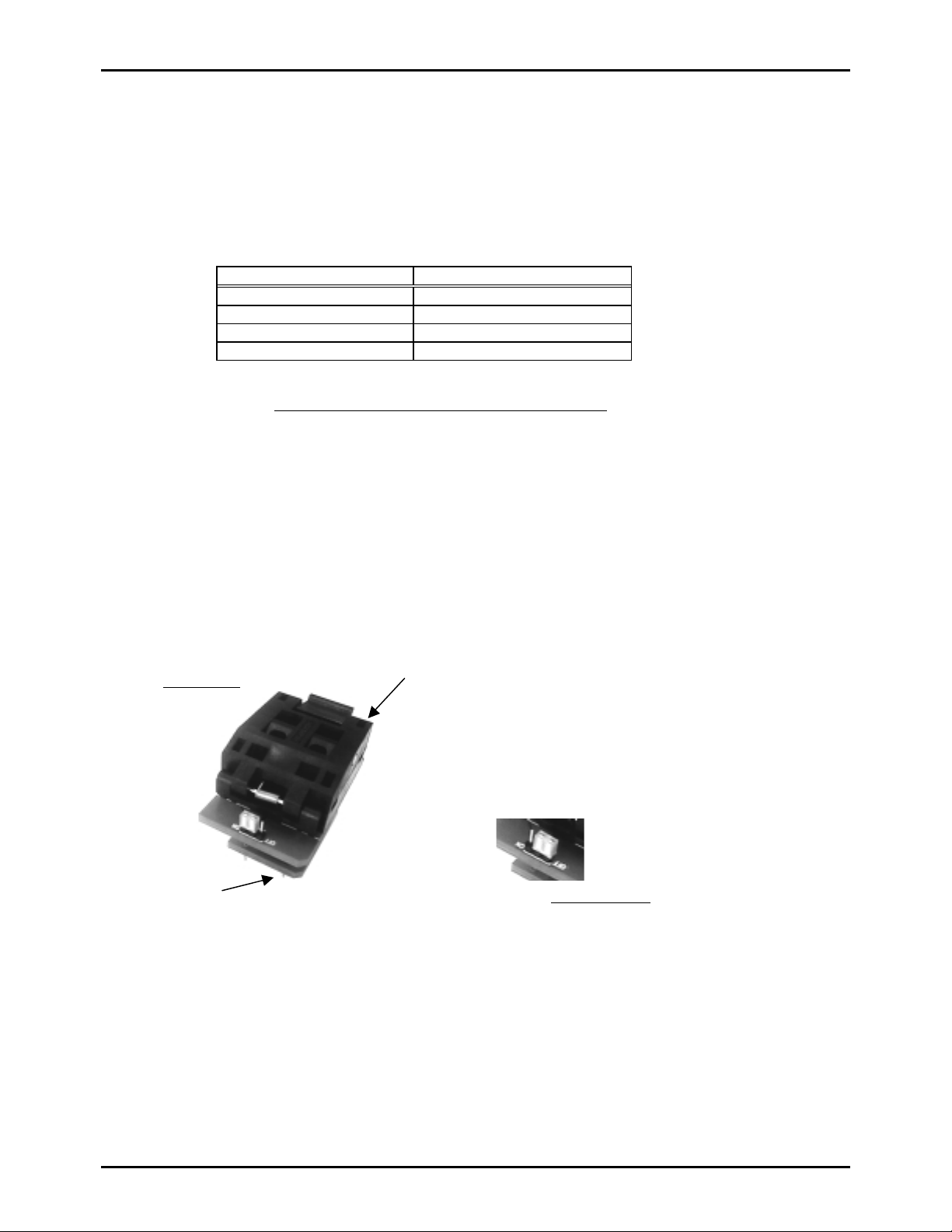
LC86E6548 can be programmed by the EPROM programmer with attachment ; W86EP6548Q.
• Recommended EPROM programmer
Productor EEPROM programmer
Advantest R4945, R4944, R4943
Andou AF-9704
AVAL PKW-1100, PKW-3000
Minato electronics MODEL 1890A
• “27512 (Vpp=12.5V) Intel high speed programming” mode available. The address must be set to
“0 to 0FFFFH” and a jumper (D ASE C) must be set to ‘OFF’ at programming
.
(3) How to use the data security function
“Data security” is the disabled function to read the data of the EPROM.
The following is the process in order to execute the data security.
1. Set ‘ON’ the jumper of attachment.
2. Program again. Then EPROM programmer displays the error. The error means normally
activity of the data security. It is not a trouble of the EPROM programmer or the LSI.
Notes
• Data security is not executed when the data of all address have ‘FFH’ at the sequence 2 above.
• The programming by a sequential operation “BLANK⇒PROGRAM⇒VERIFY” cannot be executed data security at the
sequence 2 above.
• Set to ‘OFF’ the jumper after executing the data security.
Data security
of LSI
1 pin mark
1 pin
W86EP6548Q
Not data security
(4) How to eliminate
The programming data can be erased by using the EPROM eraser.
(5) Shielding
The UVEPROM (ultraviolet erasable programmable ROM) is in it. Put the seal on the window in use.
No.6747-4/21

Pin Assignment
Z
N
N
S48/PG0
S49/PG1
S50/PG2
S51/PG3
P00
P01
P02
P03
VSS2
VDD2
P04
P05
P06
P07
P10/SO0
P11/SI0/SB0
P12/SCK0
P13/SO1
P14/SI1/SB1
P15/SCK1
LC86E6548
S47/PF7
S46/PF6
S45/PF5
S44/PF4
S43/PF3
S42/PF2
S41/PF1
S40/PF0
VDD4
S39/PE7
S38/PE6
S37/PE5
S36/PE4
S35/PE3
S34/PE2
S33/PE1
S32/PE0
S31/PD7
S30/PD6
S29/PD5
S28/PD4
S27/PD3
S26/PD2
S25/PD1
S24/PD0
8079787776757473727170696867666564636261605958575655545352
81
82
83
84
85
86
87
88
89
90
91
92
93
94
95
96
97
98
99
100
1 2 3 4 5 6 7 8 9
P30
P31
P32
P33
P16/BUZ
P17/PWM0
10
11
12
13
14
15
16
17
18
19
20
21
22
23
24
25
P34
P35
P36
P74
P37
RES
P70/INT0
CF1
CF2
VSS1
XT1/
XT2/P75
VDD1
P80/AN0
P81/AN1
P82/AN2
P83/AN3
P84/AN4
P85/AN5
P86/AN6
S23/PC7
26
P87/AN7
S22/PC6
27
P71/INT1
S21/PC5
28
P72/INT2/T0I
S20/PC4
29
P73/INT3/T0I
VP
51
30
S0/T0
50
49
48
47
46
45
44
43
42
41
40
39
38
37
36
35
34
33
32
31
S19/PC3
S18/PC2
S17/PC1
S16/PC0
VDD3
S15/T15
S14/T14
S13/T13
S12/T12
S11/T11
S10/T10
S9/T9
S8/T8
S7/T7
S6/T6
S5/T5
S4/T4
S3/T3
S2/T2
S1/T1
SANYO: QFC100S
No.6747-5/21
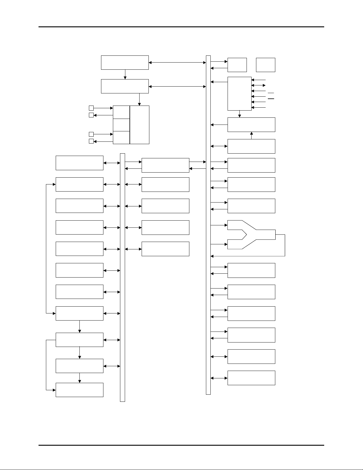
System Bl ock Diagram
Interrupt Control
Standby Control
Base Timer
SIO0
SIO1
Timer 0
Timer 1
ADC
INT0 to 3
Noise Filter
SIO Automatic
transmission
RAM
(128 bytes)
VFD controller
High voltage
Output
CF
RC
X’tal
Colck
Generator
LC86E6548
Bus Interface
Port 1
Port 3
Port 7
Port 8
IR PLA
EPROM
Control
EPROM (48KB)
PC
ACC
B Register
C Register
ALU
PSW
RAR
RAM
Stack Pointer
Port 0
Watchdog T i mer
A15-A0
D7-D0
TA
CE
OE
DASEC
No.6747-6/21
LC86E6548
LC86E6548 Pin description
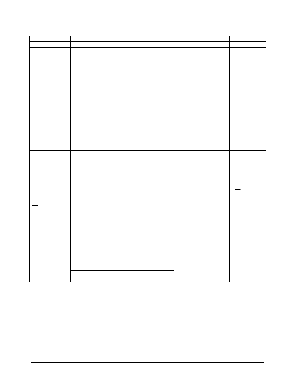
Pin name I/O Function description Option EPROM mode
VSS1,2 - Power pin (-) *4 - VDD1,2,3,4 - Power pin (+) *4 - VP - Power pin (+) for the VFD output pull-down resist - PORT0
P00 to P07
PORT1
P10 to P17
PORT3
P30 to P37
PORT7
P70 to P73
P74
to P75
I/O •8-bit input/output port
•Input for port 0 inter rupt
•Input/output in nibble units
•Input for HOL D rel ease
•15V withstand at N- channel open drain
output
I/O •8-bit input/output port
•Input/output can be specified in a bit unit
•Other pin functions
P10 SIO0 data output
P1 1 SIO 0 data input/bus input/output
P12 SIO0 clock input/output
P1 3 SIO 1 data output
P1 4 SIO 1 data input/bus input/output
P15 SIO1 clock input/output
P16 Buzzer output
P1 7 Timer 1 output (PWM0 output)
I/O •8-bit input/output port
•Input/output in bit unit
•15V withstand at N- channel open drain
output
•4-bit input/output port
•Input/output in bit un it
•2-bit input port
•Other pin functions
I/O
P70 : INT0 input/HOLD release/N-channel Tr.
I
output for watchdog timer
P71 : INT1 input/HOLD release inpu t
P72 : INT2 input/timer 0 event input
P73 : INT3 input with noise filter/timer 0 event
input
P74
: 32.768kHz crystal oscillation terminal XT1
P75 : 32.768kHz crystal oscillation terminal XT2
•Interrupt received forms, the vector addresses
rising falling rising
&
high
level
low
level
falling
INT0 enable enable disable enable enable 03H
INT1 enable enable disable enable enable 0BH
INT2 enable enable enable disable disable 13H
INT3 enable enable enable disable disable 1BH
Continue.
vector
•Pull-up resistor :
Provided/Not provided
(each nibble)
•Output form :
CMOS/N-channel open
drain (each bit)
•Output form :
CMOS/N-channel open
drain (each bit)
•Output form :
CMOS/N-channel open
drain (each bit)
-
Data line
D0 to D7
-
EPROM control
signals
DASEC (*1)
OE
(*2)
‚bE
(*3)
CE
No.6747-7/21
 Loading...