

Sanyo LC86E4332 Specifications

Ordering number: EN *5600
Preliminary
LC86E4332
CMOS LSI
LC86E4332
8-bit Single Chip Microcontroller
Overview
The LC86E4332 is a CMOS 8-bit single chip microcontroller
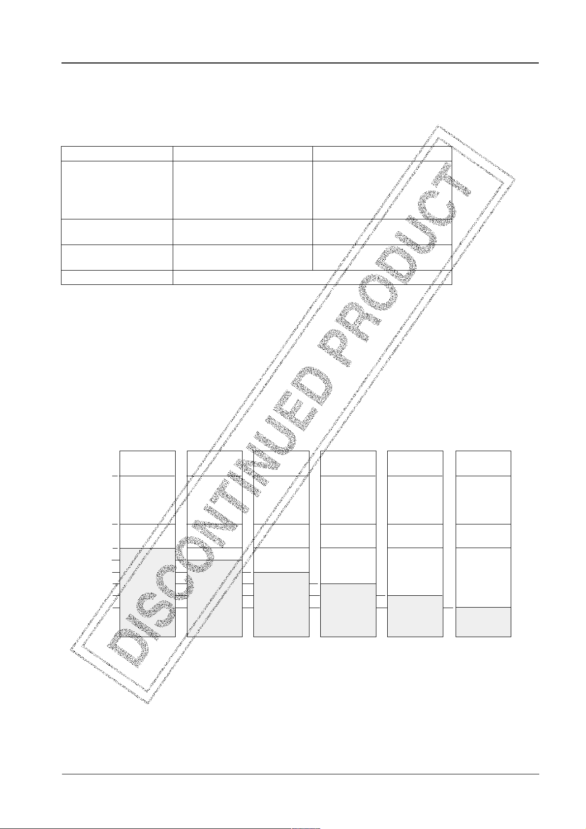
Package Dimensions
unit : mm
with UVEPROM for the LC864300 series.
This microcontroller has the function and the pin description
3225-DIC52S
of the LC864300 series mask ROM version, and the 32K-byte
EPROM. The program data is rewritable. It is suitable for
developing programs.
Features
(1) Option switching by EPROM data
The option function of the LC864300 series can be specified by the EPROM data.
The functions of the trial pieces can be evaluated using the mass production board.
(2) Internal EPROM capacity : 32768 bytes (For program)
: 16384 × 12 bits (For character)
(3) Internal RAM capacity : 384 bytes
52
14.99
1
0.9 0.46 1.778
[LC86E4332]
46.74
41.94
44.45
27
14.66
26
1.27
8.7
4.0
2.03
1.145
SANYO : DIC52S
15.24
Mask ROM version PROM capacity RAM capacity
LC864332 32512 bytes 384 bytes
LC864328 28672 bytes 384 bytes
LC864324 24576 bytes 384 bytes
LC864320 20480 bytes 384 bytes
LC864316 16384 bytes 384 bytes
LC864312 12288 bytes 384 bytes
(4) Operating supply voltage : 4.5 V to 5.5 V
(5) Instruction cycle time : 0.99 µs to 40 µs
(6) Operating temperature : +10°C to +40°C
(7) The pin and the package compatible with the LC864300 series mask ROM version.
(8) Applicable mask ROM version : LC864332/LC864328/LC864324/LC864320/LC864316/LC864312
(9) Factory shipment : DIC52S
SANYO Electric Co.,Ltd. Semiconductor Bussiness Headquarters
SANYO Electric Co., Ltd. Semiconductor LSI Div. Microcomputer Development Dep.
TOKYO OFFICE Tokyo Bldg., 1-10, 1 Chome, Ueno, Taito-ku, TOKYO, 110-8534 JAPAN
33098HA (II)
No. 5600-1/19
LC86E4332
Notice for Use
When using, take notice of the followings.
(1) Differences between the LC86E4332 and the LC864300 series
Items LC86E4332 LC864332/28/24/20/16/12
Operation after reset
releasing
The option is specified by degrees
until 3 ms after going to a 'H' level to
the reset terminal. The program is
executed from 00H of the program
counter.
Operating supply voltage
range (V
DD
)
Operating temperature range
4.5 V to 5.5 V
+10 to +40°C
(Topr)
Power dissipation Refer to 'electrical characteristics' on the semiconductor news.
Port configurations of LC86E4332 and LC864332/28/24/20/16/12 are identical during the reset operation.
The LC86E4332 uses the program memory area of 256 bytes from 7F00H to 7FFFH to select the options. All LC86E4332 series’
options can be specified with this configuration.
The program is executed from 00H
of the program counter immediately
after going to a 'H' level to the reset
terminal.
4.5 V to 5.5 V
–30 to +70°C
(2) Option
The option data is written with the option specifying program "SU86K.EXE". The option data is linked to the program area by
the linkage loader "L86K.EXE".
(3) ROM space
The LC86E4332 and LC864300 series use the program memory area of 256 bytes from 7F00H to 7FFFH to select the options.
The program memory capacity of this series is, at most, 32512 bytes addressed on 0000H to 7EFFH.
17FFFH
10000H
07FFFH
07EFFH
06FFFH
05FFFH
04FFFH
03FFFH
02FFFH
0000H
Charactor
generator ROM
Option specified
area 256 bytes
Program area
32K bytes
Charactor
generator ROM
Option specified
area 256 bytes
Program area
28K bytes
Charactor
generator ROM
Option specified
area 256 bytes
Program area
24K bytes
Charactor
generator ROM
Option specified
area 256 bytes
Program area
20K bytes
Charactor
generator ROM
Option specified
area 256 bytes
Program area
16K bytes
Charactor
generator ROM
Option specified
area 256 bytes
Program area
12K bytes
LC864332 LC864328 LC864324 LC864320 LC864316 LC864312
No. 5600-2/19

LC86E4332
How to Use
(1) Create a programming data for LC86E4332
Programming data for EPROM of the LC86E4332 is required.
Debugged evaluation file (EVA file) must be converted to an INTEL-HEX formatted file (HEX file) with the file converter
program EVA2HEX.EXE. The HEX file is used as the programming data for the LC86E4332.
(2) How to program for the EPROM
The LC86E4332 can be programmed by the EPROM programmer with attachment W86EP4164D.
• Recommended EPROM programmer
Manufacturer
Productor
Advantest
Andou
AVAL
Minato electronics
• "27010 (Vpp = 12.5 V) Intel high speed programming" mode should be adopted.
•
A jumper (DASEC) must be set to 'OFF' at programming.
• There are two ways to program the data of the hexa-decimal file described above into the EPROM of the LC86E4332.
1. How to program the program and the character data individually.
First, the hexa-decimal data of 00h to 07FFFh is programmed into the address 00h to 07FFFh of the EPROM.
Next, write the hexa-decimal data for character addressed 10000h to 17FFFh into the address of 10000h to 17FFFh.
2. How to program the program and the character data simultaneously.
First, copy the program data addressed from 00h to 07FFFh into the addresses 8000h to 0FFFFh with an EPROM
programmer.
Next, write the data of 00h to 17FFFh into the EPROM of the LC86E4332.
EPROM programmer
R4945, R4944, R4943
AF-9704
PKW-1100, PKW-3000
MODEL1890A
An error will occur when the hexa-decimal data generated by the EVA2HEX program is programmed to the EPROM of
the LC86E4332 directly.
(3) How to use the data security function
"Data security" is the function to disable the EPROM data from being read out.
The following is the process in order to execute data security function.
1. Set the jumper of attachment 'ON'.
2. Program again. The EPROM programmer will display an error. The error means that the data security functions
normally. It is not a trouble of the EPROM programmer or the LSI.
Notes
• Data security is not executed when the data of all address have 'FF' at sequence 2 above.
• Data security cannot be executed by programming the sequential operation "BLANK=>PROGRAM=>VERIFY" at
procedure 2 above.
• Set the jumper to 'OFF' after executing the data security.
Data security
Data security OFF
Jumper
Jumper
Pin 1
W86EP4164D
No. 5600-3/19
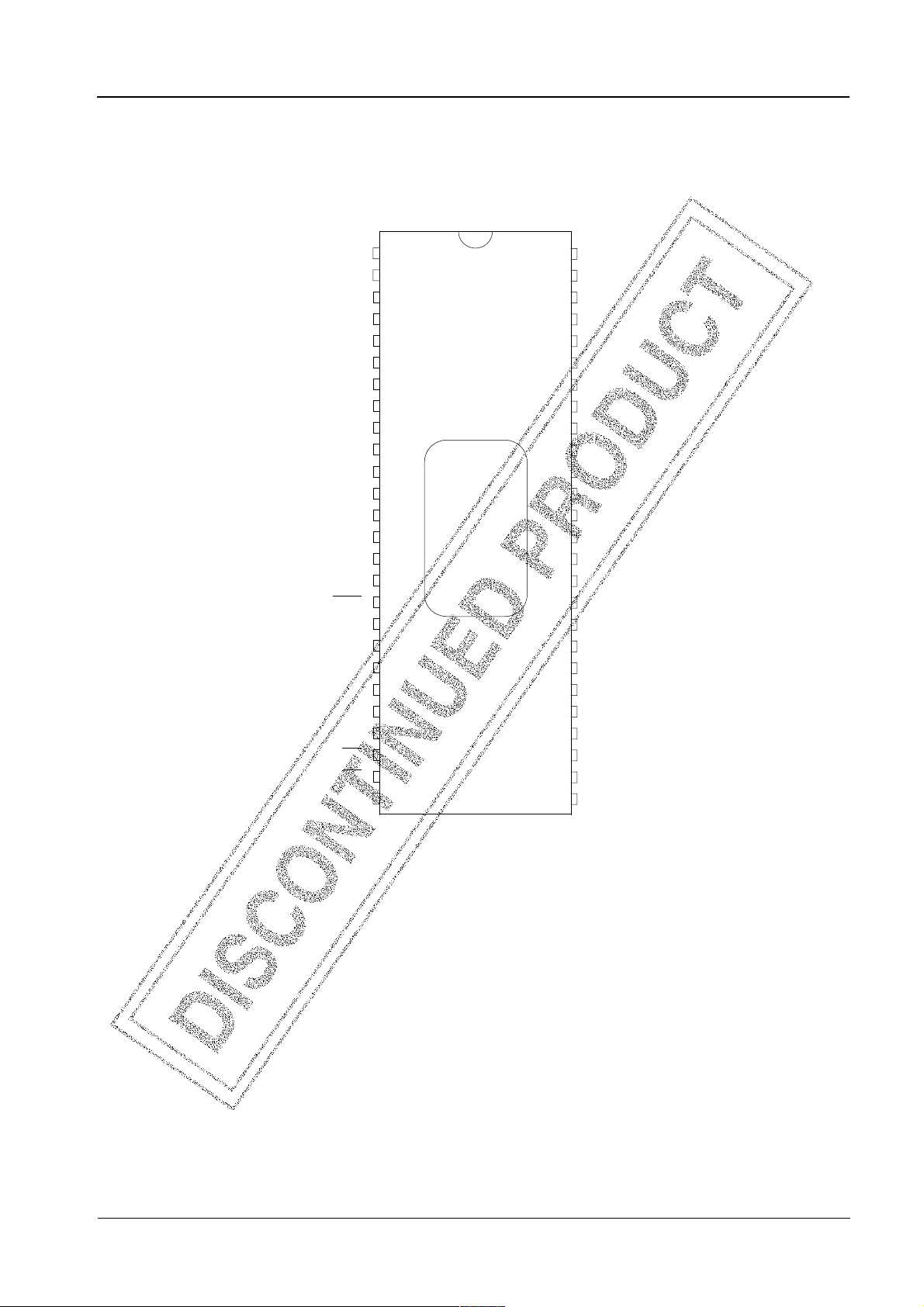
Pin Assignment
LC86E4332
P10/SO0
P11/SI0/SB0
P12/SCK0
P13
P14
P15
P16
P17/PWM
DVSS
CF1
CF2
DVDD
P90/AN0/BLIN
P91/AN1/BIN
P92/AN2/GIN
P93/AN3/RIN
RES
LC1
LC2
FILT
AVDD
AVSS
CVIN
VS
HS
1
2
3
4
5
6
7
8
9
10
11
12
13
14
15
16
17
18
19
20
21
22
23
24
25
26
I
P07
52
P06
51
P05
50
P04
49
P03
48
P02
47
P01
46
P00
45
P73/INT3/T0IN
44
P72/INT2/T0IN
43
P71/INT1
42
P70/INT0
41
PWM9
40
PWM8
39
PWM7
38
PWM6
37
PWM5
36
PWM4
35
PWM3
34
PWM2
33
PWM1
32
PWM0
31
BL
30
29
B
28
G
27
R
Top view
No. 5600-4/19

System Block Diagram
LC86E4332
SIO0
Timer 0
Timer 1
ADC
Interrupt control
Standby control
CF
RC
Colck
LC
generator
Bus interface
Port 1
Port 7
Port 9
IR PLA
EPROM
control
EPROM(32KB)
PC
ACC
B register
C register
ALU
PSW
A16 to A0
D7 to D0
TA
CE
OE
DASEC
INT0 to 3
Noise rejection filter
PWM
Data slicer
PLL
OSD
control
circuit
RAR
RAM
Stack pointer
CGROM
Port 0
VRAM
Watch dog timer
No. 5600-5/19

LC86E4332
Pin Description
• Port option can be specified by bit units.
• At port 0, 'Pull-up resistor provided' when specifying CMOS output.
'Pull-up resistor not provided' when specifying N-ch open drain output.
• At port 1, 'Programmable pull-up resistor provided' when specifying either CMOS or N-ch open drain output.
Pin Description Table
Pin name Pin No. I/O Function description Option PROM mode
DVSS 9 — Negative power supply for digital circuit
CF1 10 I Input terminal for ceramic resonator
CF2 11 O Output terminal for ceramic resonator
DVDD 12 — Positive power supply for digital circuit
RES 17 I Reset terminal
LC1 18 I LC oscillation circuit input terminal
LC2 19 O LC oscillation circuit output terminal
FILT 20 O Filter terminal for PLL
AVDD 21 — Positive power supply for analog circuit
AVSS 22 — Negative power supply for analog circuit
CVIN 23 I Video signal input terminal
VS 24 I Vertical synchronization signal input terminal
HS 25 I Horizontal synchronization signal input
terminal
I 26 O Image intensity output
R 27 O Red (R) output terminal of RGB image output A4 (*1)
G 28 O Green (G) output terminal of RGB image A5 (*1)
output
B 29 O Blue (B) output terminal of RGB image output A6 (*1)
BL 30 O Fast blanking control signal A7 (*1)
Switch TV image signal and caption/OSD
image signal
PWM0 31 to 40 O PWM0 to 9 output terminal PWM0 to 8 :
to PWM9 15 V withstand A8 to A16 (*1)
PWM9 : "L" fixed
Port 0 8-bit Input/output port Pull-up resistor
P00 to P07 45 to 52 I/O Input/output can be specified in nibble units Provided/not provided
HOLD release input (in bit units)
Interrupt input Output Format
CMOS/Nch-OD
(in bit units)
Port 1 8-bit Input/output port Output Format D0 to D7 ( *2)
P10 to P17 1 to 8 I/O Input/output can be specified in bit units. CMOS/Nch-OD
Other function (in bit units)
P10 SIO0 data output
P11 SIO0 data input /bus input/output
P12 SIO0 clock input/output
P17 Timer 1 (PWM) output
No. 5600-6/19
 Loading...