

SANYO LC868116A, LC868112A, LC868108A Datasheet

Ordering number : ENN*6724
CMOS IC
LC868116/12/08A
8-Bit Single Chip Microcontroller with
16/12/08K-Byte ROM and 640-Byte RAM On Chip
Preliminary
Overview
The LC868116A/12A/08A microcontrollers are 8-bit single chip microcontrollers with the following on-chip functional
blocks :
- CPU : Operable at a minimum bus cycle time of 0.5µs (microseconds)
- On-chip ROM maximum capacity : 16K bytes
- On-chip RAM capacity : 640 bytes
- Dot-matrix liquid crystal display (LCD) automatic display controller / driver
- Externa l memory
- 16-bit timer / counter (or two 8-bit timers)
- 16-bit timer / PWM (or two 8-bit timers)
- Two 8-bit synchronous serial -interface circuits
- 13-source 9-level vectored interrupt system
All of the above functions are fabricated on a single chip
Ver.1.1
21998
91400 RM (IM) HO No.6724-1/28
LC868116/12/08A
Features
(1) Read Only Memory (ROM) : LC868116A 16384 × 8 bits
: LC868112A 12288 × 8 bits
: LC868108A 8192 × 8 bits
(2) Random Access Memory (RAM) : 512 × 8 bits (calculation area)
128
8 bits (display area)
×
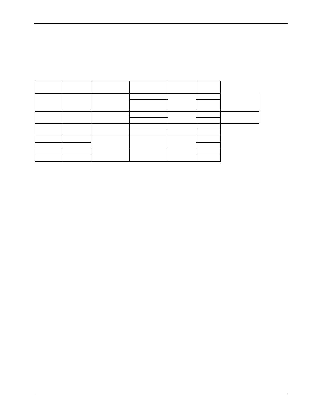
(3) Bus Cycle Time / Instruction Cycle Time
Bus cycle
time
0.5µs 1µs
1µs 2µs
2µs 4µs
7.5µs 15µs
3.8µs 7.5µs
183µs 366µs
91.5µs 183µs
Instruction
cycle time
System clock
oscillation
Ceramic (CF)
Oscillation
Voltage Note
frequency
12MHz OCR7=0
4.5-6.0V
6MHz
Ceramic (CF)
6MHz OCR7=0
4.5-6.0V
3MHz
Ceramic (CF)
3MHz OCR7=0
2.5-6.0V
1.5MHz
Internal RC 800kHz 2.5-6.0V
Crystal (XTAL) 32.768kHz 2.5-6.0V
OCR7=1
OCR7=1
OCR7=1
OCR7=0
OCR7=1
OCR7=0
OCR7=1
* Bus cycle time means ROM-read period.
OCR7 : Bit-7 of the oscillation control register.
(4) Ports
- Input / output ports : 6 ports (47 terminals)
Input/output port programmable in a nibble : 1 port (8 terminals)
Input/output port programmable every function unit : 1 port (7 terminals)
Input/output port programmable in a bit : 4 ports (32 terminals)
- Input port : 1 port (4 terminals)
- Ports at external memory mode
1. External Latch
Port 0 : Address output of lower 8-bit, input/output of data
Port 2 : Address output of upper 8-bit
Port 5 : Bank address output
2. No External Latch
Port 0 : Input/output of data
Port 3 : Address output of lower 8-bit
Port 2 : Address output of upper 8-bit
Port 5 : Bank address output
(Set whether the external latch is used or not by program.)
- LCD segment driver output ports : 48 terminals
(Function change available : segment/common)
- LCD common driver output ports : 16 terminals
(1/32 duty maximum : at using segment output ports as common output by mask option)
(5) External memory access
- Externa l progra m memor y acce ss function
External program memory capacity : 64K bytes
Programable switch internal program/external program
(At initial : Internal program)
Enable/disable control of external program ! internal p rogr am memo ry switch
excluding
external memory
access function
for external
memory acce ss
No.6724-2/28

LC868116/12/08A
- Ports
Port 2 : Address output of upper 8-bit
Uses
EROE terminal (OE signal of the external ROM)
1. Using the external latch
Port 0 : Address output of lower 8-bit, data input port
Uses the ADLC terminal (latch clock of the lower 8-bit address signal)
2. Not use the external latch
Port 0 : Input port of data
Port 3 : Addres s output of lowe r 8-bit
- External data memory access function
Using the LDC instruction
External memory capacity : 16M bytes
1. Internal prog ram memory
Switch the reference of internal ROM data/external ROM data by program.
2. External program memory
Reference external ROM data only.
Ports
Port 2 : Address output of upper 8-bit
Port 5 : Bank address output
Uses
EROE terminal (OE signal of the external ROM)
1. Using external latch
Port 0 : Address output of lower 8-bit, input port of data
Uses the ADLC terminal (latch clock of the lower 8-bit address signal)
2. Not use external latch
Port 0 : Input port of data
Port 3 : Addres s output of lowe r 8-bit
- External RAM memory access function
Using the LDX, STX instruction
External memory capacity : 16M bytes
Ports
Port 2 : Address output of upper 8-bit
Port 5 : Bank address output
Uses the P46 terminal (
Uses the P47 terminal (
OE signal of external RAM) : the LDX instruction execution
WE signal of external RAM) : the STX instruction execution
1. Using the external latch circuit
Port 0 : Address output of lower 8-bit, input/output port of data
Uses the ADLC terminal (latch clock of the lower 8-bit address signal)
2. Not use the external latch circuit
Port 0 : Input/output port of data
Port 3 : Addres s output of lowe r 8-bit
(6) LCD automatic display controller
- Display duty : 1/4 - 1/32 duty
* Up to 1/32 display duty can be specified by program. V DD allows up to 6V. Select the preferable LCD panel within
this range.
- Displ ay bias : 1/4, 1/5, 1/ 7 bias
- Programmable character display / graphic display
- Character display
1. On-chip char acter generator ROM
ROM capacity : 8960 bits
Character font : 5 × 7 dots
Number of Characters : 256
No.6724-3/28
LC868116/12/08A
2. LCD instruction
Display : ON/OFF
Cursor : ON/OFF/BLINK
Character blink : ON/OFF
Character scroll : Control by specified starting address
- Graphic display
LC868100 series : 1024 dots Maximum
External segment driver : Enable to extend of LCD drive
- LCD contrast
LCD display contrast programmable
- LCD display power supply
Doubler circuit available wi thin VDD≤3V.
* Doubler generates up to 6V.
- LCD driver
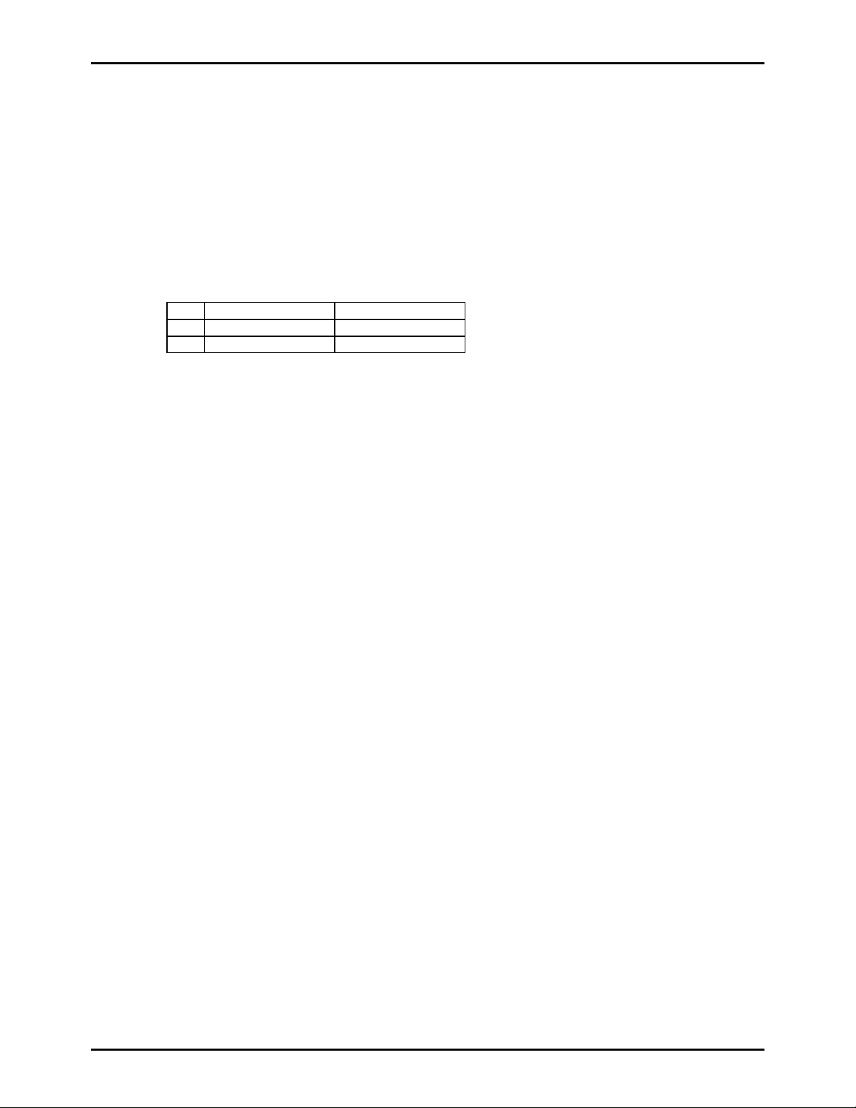
Following two kinds of combination can be selected by mask option
No. Segment output port Common output port
1 48 16
2 32 32
* Up to 32 commons can be specified by mask option. As maximum LCD display voltage is 6V, please select
the preferable LCD panel and the display condition with this range.
* In general, the LCD driver cannot be expanded.
(7) Serial-interface
- Two 8-bit serial-interf ace circuits
LSB first / MSB first function available
- Internal 8-bit baud-rate generator in common with two serial-interface circuits
(8) Timers
- Timer0 (T0L, T0H)
16-bit timer / counter
2-bit prescaler + 8-bit programmable prescaler
Mode 0 : Two 8-bit timers with programmable prescaler
Mode 1 : 8-bit timer with a programmable prescaler + 8-bit counter
Mode 2 : 16-bit timer with a programmable prescaler
Mode 3 : 16-bit counter
- Timer1 (T1L, T1H)
16-bit timer / PWM
Mode 0 : Two 8-bit timers
Mode 1 : 8-bit timer + 8-bit PWM
Mode 2 : 16-bit timer
Mode 3 : Variable-bit PWM (9-16 bits)
- Base timer
Every 500ms overflow system for a clock application (using 32.768kHz crystal oscilla tion for Base timer clock)
The Base timer clock selectable ; 32.768kHz crystal oscillation, System clock, and programmable prescaler output of
Timer 0
(9) Buzzer output
- The Buzzer sound frequency selectable ; 4KHz, 2KHz
(10) Remote control receiver circuit (using P73/INT3/T0IN terminal)
- Noise rejection available
- The interrupt polarity selectable
No.6724-4/28

LC868116/12/08A
(11) Watchdog timer
- The watchdog timer is taken on RC outside. (using P70/INT0 terminal)
- Watchdog timer operation selectable : interrupt system, system reset
(12) Interrupts system
- 13-source 9-level vectored interrupts :
1. External interrupt INT0 (includes watchdog timer)
2. External interrupt INT1
3. External interrupt INT2, timer / counter T0L (timer 0 lower 8 bits)
4. External interrupt INT3, base timer
5. Timer / counter T0H (timer 0 upper 8-bit)
6. Timer T1L (timer 1 lower 8-bit), Timer T1H (timer 1 upper 8-bit)
7. Serial interface SIO0
8. Serial interface SIO1
9. Port 0 or Port 3
- Interrupt priority contr ol availa b le
Microcomputer allows 3 levels of interrupt; low level, high level and highest level of multiplex interrupt. It can specify
a low level or a high level interrupt priority from INT2/T0L through port 0 or port 3 (the above interrupt number from
three through nine). It can also specify a low level or the highest level interrupt priority to INT0 and INT1.
(13) Sub-routine stack levels
- 128 levels (Max.) : stack area included in RAM area
(14) Multiplication and division
- 16 bits × 8-bit (7 instruction cycle times)
- 16 bits / 8-bit (7 instruction cycle times)
(15) Three oscillation circuits
- On-chip RC oscillation circuit using for the system clock, for the LCD display and for the step-up circuit.
- On-chip CF oscillation circuit using for the system clock, for the LCD display and for the step-up circuit.
- On-chip crystal oscillation circuit using for the system clock, for time-base clock and for the LCD display.
(16) Standby function
- HALT mode function
The HALT mode is used to reduce the power dissipation. In this operation mode, the program execution is stopped.
This operation mode can be released by the interrupt request signals or setting to low level for the reset terminal
RES).
(
- HOLD mode function
The HOLD mode is used to freeze all the oscillations ;
RC (internal), CF and Crystal oscillations. This mode can be released by the following operations:
• Reset terminal (
RES) set to low level.
• Set to assigned level to INT0/1 terminals.
• Set to assigned level to Port 0/3.
(17) Factory shipment
- Chip
QIC160 package shipping available for sample evaluation.
(18) Development support tools
- Evaluation (EVA) chip : LC868099
- Emulator : EVA86000 + ECB868000 (Evaluation chip board)
No.6724-5/28
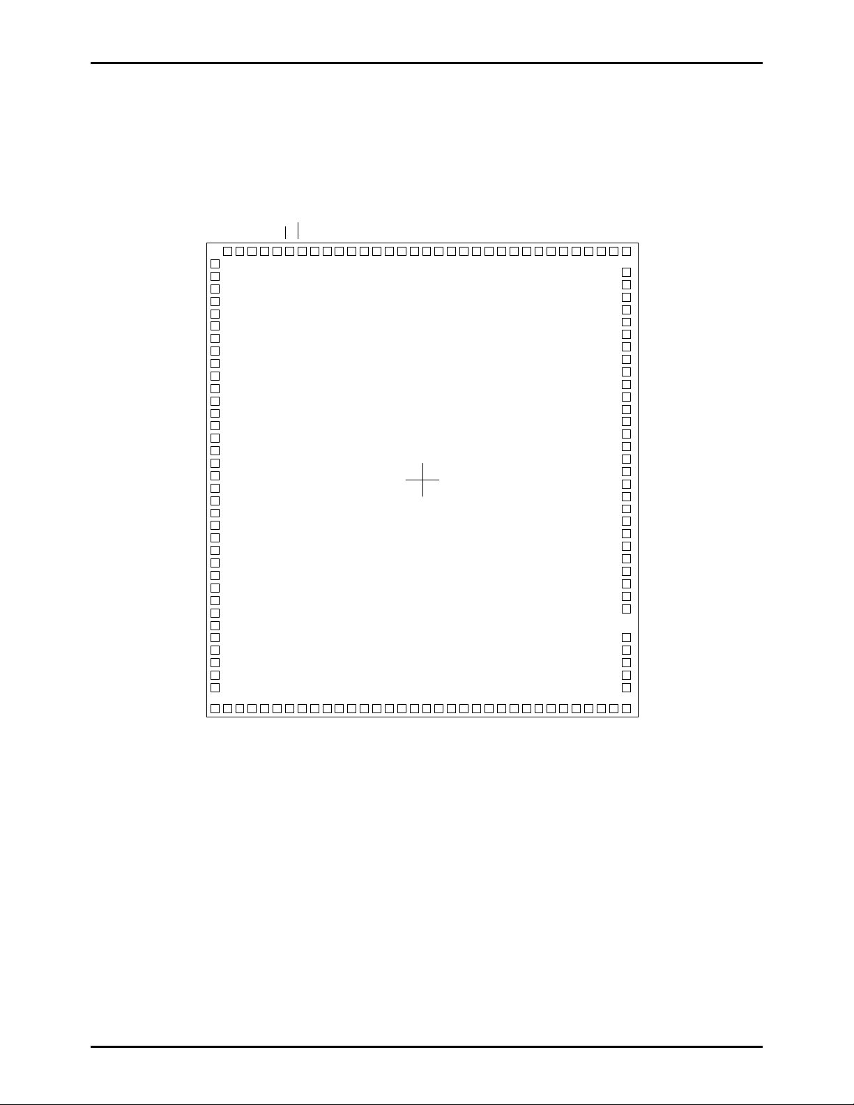
Pin Assignment
Chip size : 4.98mm × 6.26mm
Pad size : 106µm × 106µm
Bonding area size : 90µm × 90µm
Chip thickness : 480µm±20µm
CF2
CF1
VSS
XT2
XT1
RES
EROE
ADLC
P27
LC868116/12/08A
P26
P25
P24
P23
P22
P21
P20
P07
P06
P05
P04
P03
P02
P01
P00
P37
P36
P35
P34
P33
P32
P31
P30
VDD
VDD
S10
S11
S12
S13
S14
S15
S16
S17
S18
S19
S20
S21
S22
S23
S24
S25
S26
S27
S28
S29
S30
S31
S32
S33
S34
S1
S2
S3
S4
S5
S6
S7
S8
S9
(0, 0)
P50
P51
P52
P53
P54
P55
P56
P57
P17
P16
P15
P14
P13
P12
P11
P10
P73
P72
P71
P70
P47
P46
P44
P43
P42
P41
P40
VSS
CUP1
CUP2
VOUT2
VLCD
V5
S35C7S36
S37
S38
S39
S40
S41
S42
S43
S44
S45
S46
S47
S48
C16
C15
C14
C13
C9C8C6C5C4C3C2C1V1
C12
C11
C10
V2
V4
V3
No.6724-6/28
LC868116/12/08A
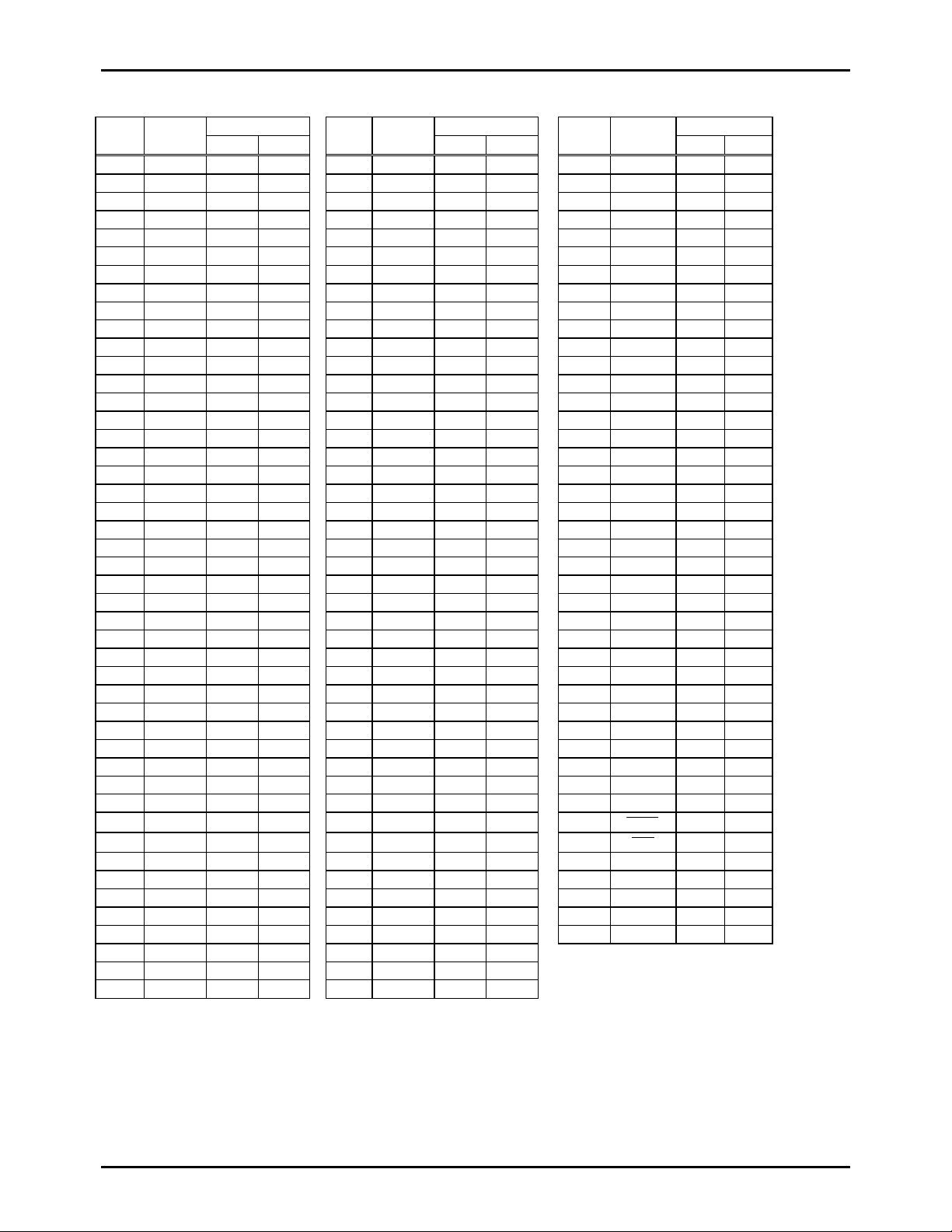
Pad Name and coordinates table
Pad
No.
Name
Coordinates Coordinates Coordinates
Xµm Yµm
Pad
No.
Name
Xµm Yµm
1 VDD -2240 2236 47 S46 -700 -2875 93 P16 2240 960
2 S1 -2240 2100 48 S47 -565 -2875 94 P17 2240 1096
3 S2 -2240 1965 49 S48 -429 -2875 95 P57 2240 1231
4 S3 -2240 1829 50 C16 -293 -2875 96 P56 2240 1367
5 S4 -2240 1694 51 C15 -158 -2875 97 P55 2240 1502
6 S5 -2240 1558 52 C14 -22 -2875 98 P54 2240 1638
7 S6 -2240 1422 53 C13 113 -2875 99 P53 2240 1774
8 S7 -2240 1287 54 C12 249 -2875 100 P52 2240 1909
9 S8 -2240 1151 55 C11 385 -2875 101 P51 2240 2045
10 S9 -2240 1016 56 C10 520 -2875 102 P50 2240 2180
11 S10 -2240 880 57 C9 656 -2875 103 VDD 2123 2875
12 S11 -2240 744 58 C8 791 -2875 104 P30 1987 2875
13 S12 -2240 609 59 C7 927 -2875 105 P31 1852 2875
14 S13 -2240 473 60 C6 1063 -2875 106 P32 1716 2875
15 S14 -2240 338 61 C5 1198 -2875 107 P33 1581 2875
16 S15 -2240 202 62 C4 1334 -2875 108 P34 1445 2875
17 S16 -2240 66 63 C3 1469 -2875 109 P35 1309 2875
18 S17 -2240 -69 64 C2 1605 -2875 110 P36 1174 2875
19 S18 -2240 -205 65 C1 1741 -2875 111 P37 1038 2875
20 S19 -2240 -340 66 V1 1876 -2875 112 P00 903 2875
21 S20 -2240 -476 67 V2 2012 -2875 113 P01 767 2875
22 S21 -2240 -612 68 V3 2147 -2875 114 P02 631 2875
23 S22 -2240 -747 69 V4 2283 -2875 115 P03 496 2875
24 S23 -2240 -883 70 V5 2240 -2479 116 P04 360 2875
25 S24 -2240 -1018 71 VLCD 2240 -2344 117 P05 225 2875
26 S25 -2240 -1154 72 VOUT2 2240 -2208 118 P06 89 2875
27 S26 -2240 -1290 73 CUP2 2240 -2072 119 P07 -47 2875
28 S27 -2240 -1425 74 CUP1 2240 -1937 120 P20 -182 2875
29 S28 -2240 -1561 75 VSS 2240 -1481 121 P21 -318 2875
30 S29 -2240 -1696 76 P40 2240 -1345 122 P22 -453 2875
31 S30 -2240 -1832 77 P41 2240 -1210 123 P23 -589 2875
32 S31 -2240 -1968 78 P42 2240 -1074 124 P24 -725 2875
33 S32 -2240 -2103 79 P43 2240 -938 125 P25 -860 2875
34 S33 -2240 -2239 80 P44 2240 -803 126 P26 -996 2875
35 S34 -2240 -2374 81 P46 2240 -667 127 P27 -1131 2875
36 S35 -2192 -2875 82 P47 2240 -532 128 ADLC -1267 2875
37 S36 -2056 -2875 83 P70 2240 -396 129
38 S37 -1921 -2875 84 P71 2240 -260 130
39 S38 -1785 -2875 85 P72 2240 -125 131 XT1 -1674 2875
40 S39 -1649 -2875 86 P73 2240 11 132 XT2 -1809 2875
41 S40 -1514 -2875 87 P10 2240 146 133 VSS -1945 2875
42 S41 -1378 -2875 88 P11 2240 282 134 CF1 -2081 2875
43 S42 -1243 -2875 89 P12 2240 418 135 CF2 -2216 2875
44 S43 -1107 -2875 90 P13 2240 553
45 S44 -971 -2875 91 P14 2240 689
46 S45 -836 -2875 92 P15 2240 824
The values (X, Y) indicate the coordinates of each pad center with the center of the chip as the origin.
Connect the substrate of chip to VSS or open.
Pad
No.
Name
EROE
RES
Xµm Yµm
-1403 2875
-1538 2875
No.6724-7/28
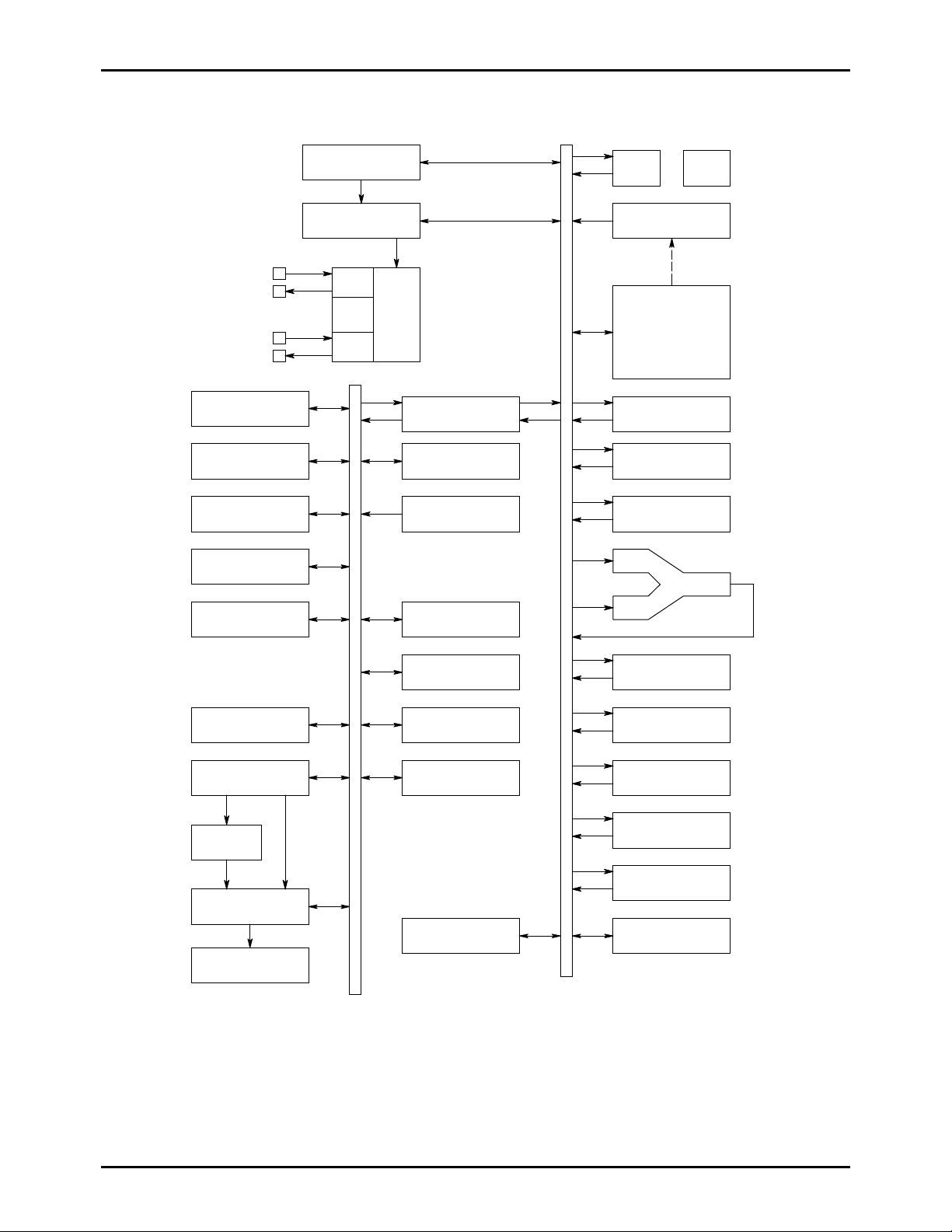
System Bl ock Diagram
LC868116/12/08A
Base Timer
SIO0
SIO1
Timer 0
Interrupt Control
Standby Control
CF
RC
Clock
X'tal
Generator
Bus Interface
Port 1
Port 7
IR PLA
ROM
PC
ACC
B Register
C Register
ALU
Timer 1
INT0-3
Noise Rejection Filter
XRAM
128 Bytes
CGROM
LCD Display
Controller
LCD Driver
Port 2
Port 3
Port 4
Port 5
EXT Register Watchdog Timer
PSW
RAR
RAM
Stack Pointer
Port 0
No.6724-8/28
LC868116/12/08A
Pin Description
Name No. I/O Function description Option
VSS 75,133 - Power terminal (-) VDD 1,103 - Power terminal (+) VLCD 71 - Power terminal (+) for LCD driver *2 V1 to V5 66-70 - Voltage supply terminals to LCD drivers *2 VOUT2 72 -
Output terminals for doubler VOUT2 ≅ 2X(VDD-VSS)
CUP1,2 74,73 - Capacitor connecting terminals for doubler, tripler Port0
P00 to P07
112-119
I/O •8-bit input/output port
•Input/output can be specified in 4-bit
•External memory mode
1. EXT resistor bit 2=0
•Pull-up resistor :
Provided/Not provided
•Output form :
CMOS/N-ch open drain
Address output of lower 8-bit, input/output
of data
2. EXT resistor bit 2=1
•Input/output of data
•Input for key interrupt (P30INT=0) *1
Port1
P10 to P17
87-94
•8-bit input/output port
I/O
•Input/output can be specified in a bit
•Output form :
CMOS/N-ch open drain
•Another functions
P10
SIO0 data output
P11
SIO0 data input, bus input/output
P12
SIO0 clock input/output
P13
SIO1 data output
P14
SIO1 data input, bus input/output
P15
SIO1 clock input/output
P16
Buzzer output
P17
Timer 1 output (PWM output)
Port2
P20 to P27 120-127
I/O •8-bit input/output port
•Input/output can be specified in a bit
•Output form :
CMOS/N-ch open drain
•External memory mode
Address output of upper 8-bit
Port3
P30 to P37 104-111
I/O •8-bit input/output port
•Input/output in a bit
•External memory mode
1. EXT resistor bit 2=0 : input/output port
•Pull-up resistor :
Provided/Not provided
•Output form :
CMOS/N-ch open drain
2. EXT resistor bit 2=1 : address output of lower
8-bit for external memory
•Input for key interrupt (P30INT=L) *1
*1 P30INT : Bit 0 of Port 3 interrupt control register.
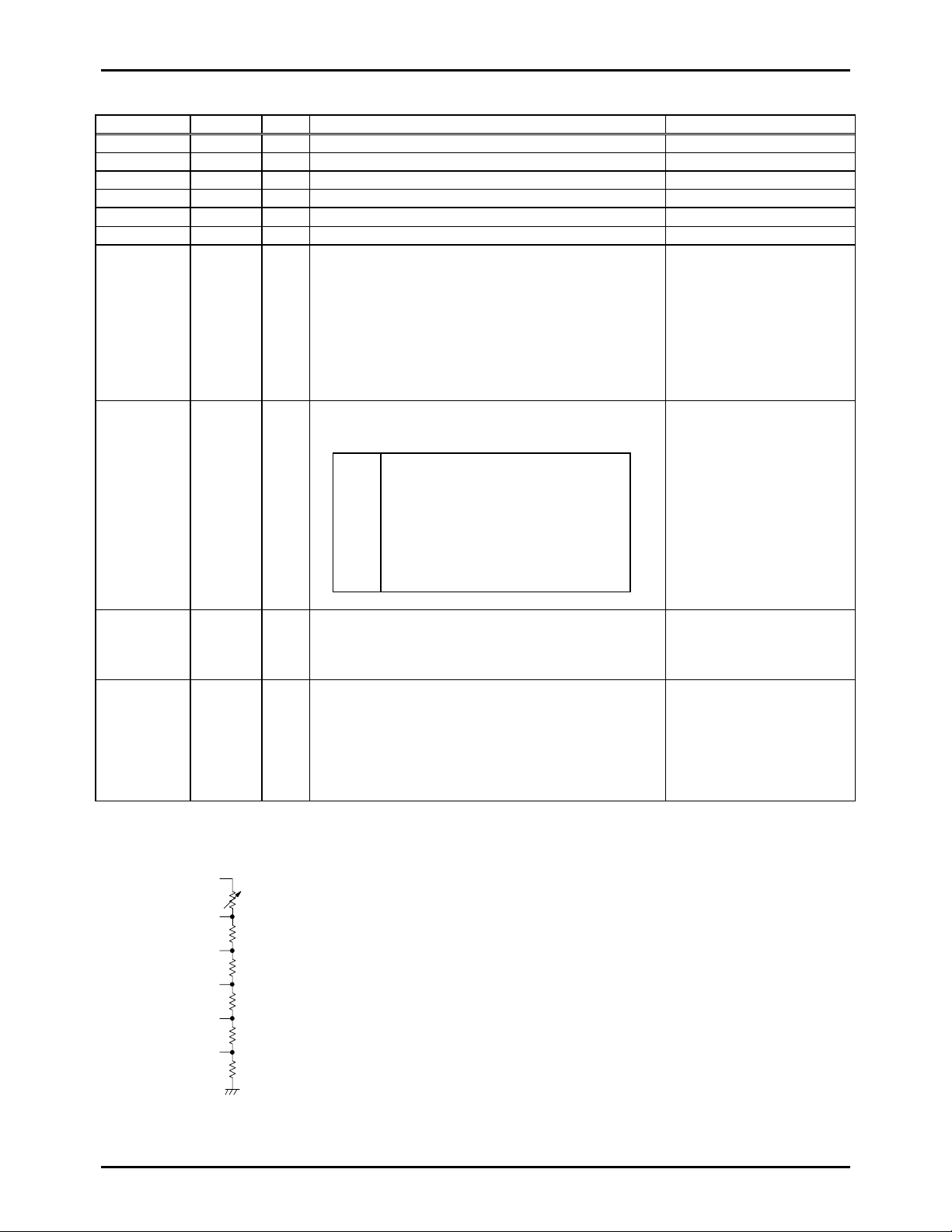
*2 The structure of the LCD power supply is shown below.
VLCD
V5
V4
V3
Resistor for
LCD contrast
adjustment
Note : If the microcontroller is operated at 3V, the voltage doubler
output (VOUT2) should be connected to the LCD power
terminal (VLCD ) .
(o r the output of an external voltage doubler should be
connected to VLCD)
V2
V1
VSS
No.6724-9/28
 Loading...