

Ordering number : ENN*6697
LC865520B/16B/12B/08B/04B
8-Bit Single Chip Microcontroller with On-Chip
20/16/12/08/04K-Byte ROM and 512-Byte RAM
Preliminary
Overview
The LC865520B/16B/12B/08B/04 B are 8-bit single chip microcontrollers with the following one-chip features:
- CPU : Operable at a minimum bus cycle time of 0.5µs
- On-chip ROM Capacity : 20K/16K/12K/8K/4K bytes
- On-chip RAM Capacity : 512 bytes (LC865520B/16B/12B/08B/04B)
- 16-bit timer/counter (can be divided into two 8 bit timers)
- 16-bit timer/PWM (can be divided into two 8 bit timers)
- 8-channel × 8-bit AD converter
- Two 8-bit synchronou s serial-interface circuits
- 13-source 10-vectored interrupt system
Features
(1) Read Only Memory (ROM) : LC865520B 20480 × 8 bits
: LC865516B 16384
: LC865512B 12288
: LC865508B 8192
: LC865504B 4096
(2) Random Access Memory (RAM) : LC865520B/16B/12B/08B/04B 512 × 8 bits
(3) Bus Cycle Time/Instruction Cycle Time
8 bits
×
8 bits
×
8 bits
×
8 bits
×
The LC865520B/16B/12B/08B/04B are constructed to read ROM twice within one instruction cycle.
It has 1.7 times the performance capability for the same instruction cycle compared to our 4-bit
microcontrollers (LC66000 series).
Bus cycle time indicates the speed to read ROM.
Bus cycle time Instruction cycle time Clock divider System clock oscillation Oscillation Frequ ency Voltage
0.5µs
2µs
7.5µs
183µs
1µs
4µs
15µs
366µs
1/1 Ceramic (CF) 6MHz 4.5V to 6.0V
1/2 Ceramic (CF) 3MHz 2.5V to 6.0V
1/2 Internal RC 800kHz 2.5V to 6.0V
1/2 Crystal (XTAL) 32.768kHz 2.5V to 6.0V
CMOS IC
Ver.1.02
32300
11901 RM (IM) Chigira No.6697-1/21

LC865520B/16B/12B/08B/04B
(4) Ports
- Input/output ports : 3 ports (16 terminals : port 1,7,8)
Input/output programmable for each bit individually
- Maximum 15V withstand tolerance input/output port : 2 p or ts (15 terminals)
Input/output programmable in nibble units : 1 port (8 terminals : port 0)
(When the N-channel open drain output is selected, input/output can be specified by bit.)
Input/output programmable for each bit individually : 1 port (7 terminals : port 3)
- Input ports : 2 ports (6 terminals : port 7,8)
(5) AD converter
- 8-channel × 8-bit AD converter
(6) Serial interface
- 1 channel × 16-bit serial interface (8-bit transm is s ion available by program)
- 1 channel × 8-bit serial interface
LSB first/MSB first-f u nction available
- An internal 8-bit baud-rate generator is common to both serial-interface circuits.
(7) Timer
- Timer 0
16-bit timer/counter
2-bit prescaler + 8-bit programmable prescaler
Mode 0 : Two 8-bit timers with programmable prescaler
Mode 1 : 8-bit timer with programmable prescaler + 8-bit counter
Mode 2 : 16-bit timer with programmable prescaler
Mode 3 : 16-bit counter
The resolution of Timer is t
CYC. (tCYC: cycle time)
- Timer 1
16-bit timer/PWM
Mode 0 : Two 8-bit timers
Mode 1 : 8-bit timer + 8-bit PWM
Mode 2 : 16-bit timer
Mode 3 : Variable-bit PWM (9-16bits)
In Mode 0 and Mode 1, the resolution of Timer and PWM is t
In Mode 2 and Mode 3, the resolution of Timer and PWM is selectable by program: t
CYC.
CYC or 1/2 tCYC.
- Base timer
Generates an overflow every 500ms for a clock application (using 32.768kHz crystal oscillation for the base timer
oscillator).
Generates an overflow every 976µs, 3.9ms, 15.6ms or 62.5ms (using 32.768kHz crystal oscillation for the base timer
clock)
Clock for the base timer is selectable from 32.768kHz crystal oscillation, system clock, or programmable prescaler
output of Timer 0.
(8) Buzzer output
- Built-in 4KHz and 2KHz buzzer generation function (using 32.768kHz crystal oscillation for the base timer oscillator)
(9) Remote receiver circuit (share with P73/INT3/T0IN terminal)
- Noise Rejection function (The filtering time of the noise rejection filter (1tCYC/16tCYC/64tCYC) can be switched by
program.) (t
CYC: instructio n-c ycle-tim e
)
- Polarity switch function
(10) Watchdog timer
- External RC circuit is required.
- Interrupt or system reset is activated when the timer overflows.
No.6697-2/21

LC865520B/16B/12B/08B/04B
(11) Interrupt
- 13-source and 10-vectored interrupt function:
1. External interrupt INT0 (including watchdog timer)
2. External interrupt INT1
3. External interrupt INT2, Timer/counter T0L (lower 8 bits of Timer 0)
4. External interrupt INT3, Base timer
5. Timer/counter T0H (upper 8 bits of Timer 0)
6. Timer T1L (lower 8 bits of Timer 1), Timer T1H (upper 8 bits of Timer 1)
7. Serial interface SIO0
8. Serial interface SIO1
9. AD converter
10. Port 0
- Built-i n I nterrupt Priority control r egister
Three interrupt priorities are supported (low, high and highest) and multi-level nesting is possible. Low or high
priority level can be assigned to the 11 interrupt sources of interrupts 3 to 10 shown above by the interrupt priority
control register. For the external interrupt INT0 and INT1(interrupt 1 and 2), low or highest can be set regardless of
the interrupt priority register.
(12) Sub-routine stack levels
- A maximum of 128 levels (set stack inside RAM)
(13) Multiplication and division
16 bits × 8-bit (7 instruction-cycle-times)
16 bits / 8-bit (7 instruction-cycle-times)
(14) 3 types of oscillation circuits
- Built-in RC oscillation circuit used for the system clock.
- CF oscillation circuit used for the system clock.
- Crystal oscillation circuit used for the system clock and the time-base clock.
(15) Standby function
- HALT mode
The HALT mode stops the program execution, which minimizes power consumption. This operation mode can be
released b y a system reset or an interrupt req ue st.
- HOLD mode
The HOLD mode stops all oscillation circuits: CF, RC and Crystal oscillations. This mode can be released by the
following conditions.
• Feed "L" level to the reset terminal (
RES )
• Feed the selected level to P70/INT0, P71/INT1 terminals
• Feed "L" level to the Port 0
(16) Shipping form
• DIP42S
• QIP48E
(17) Development tools
Evaluation (EVA) chip : LC866096
EPROM version : LC86E5420
One time version : LC86P5420
Emulator : EVA-86000 + ECB867100 (Evaluation chip board) + POD865 400 (POD)
No.6697-3/21

LC865520B/16B/12B/08B/04B
Notice for use
1. The following must be taken into consideration by the user:
Oscillation frequency range for system clock. Supply voltage range Clock Divider
15kHz to 30kHz 1/1 Can not use 1/2 divider
30kHz to 6MHz
15kHz to 30kHz 1/1 Can not use 1/2 divider
30kHz to 1.5MHz 1/1,1/2
1.5MHz to 3MHz
4.5V to 6.0V
2.5V to 6.0V
4.5V to 6.0V 1/1,1/2 Internal RC oscillation
2.5V to 6.0V 1/2 Can not use 1/1 divider
Notes
1/1,1/2
1/2 Can not use 1/1 divider
No.6697-4/21
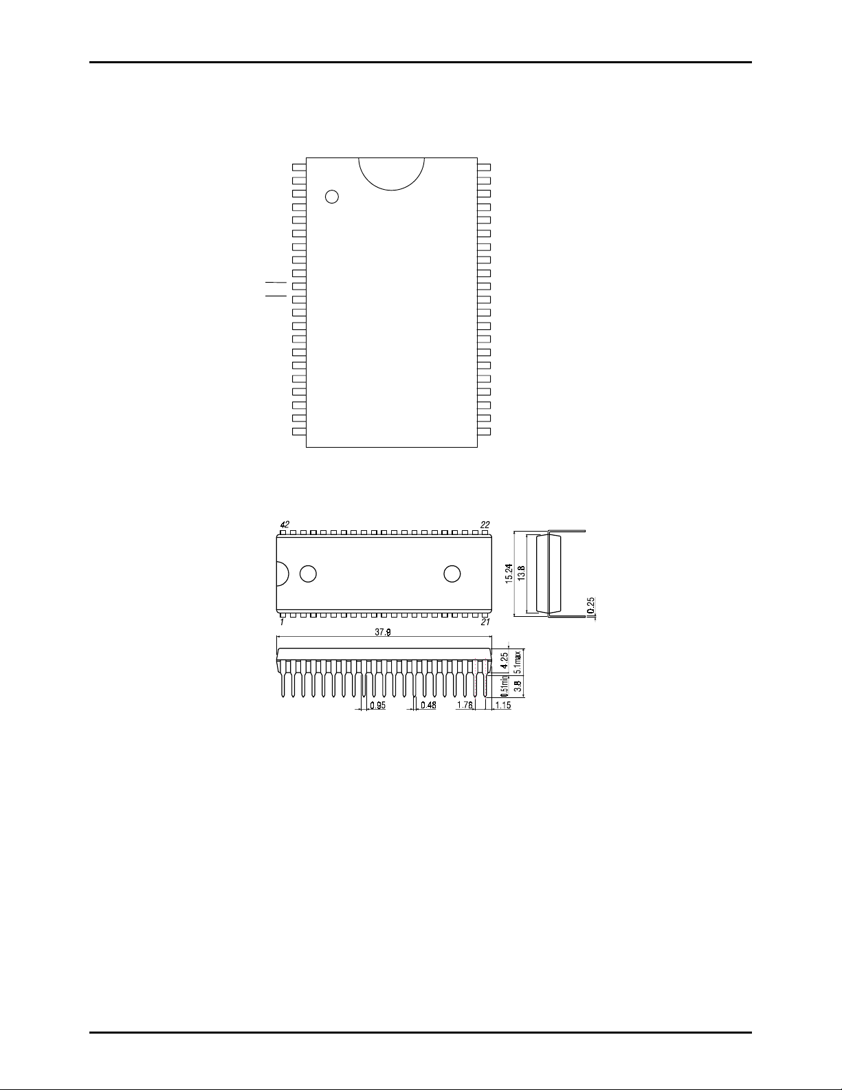
Pin Assignment
•DIP42S
Package Dimension
(unit : mm)
3025B
P00
P01
P02
P03
P04
P05
P06
P07
P70/INT0
RES
XT1/P74
XT2/P75
VSS
CF1
CF2
VDD
P80/AN0
P81/AN1
P82/AN2
P83/AN3
P84/AN4
LC865520B/16B/12B/08B/04B
1
2
3
4
5
6
7
8
9
10
11
12
13
14
15
16
17
18
19
20
21
42
41
40
39
38
37
36
35
34
33
32
31
30
29
28
27
26
25
24
23
22
P17/PWM0
P16/BUZ
P15/SCK1
P14/SI1/SB1
P13/SO1
P12/SCK0
P11/SI0/SB0
P10/SO0
P36
P35
P34
P33
P32
P31
P30
P73/INT3/T0IN
P72/INT2/T0IN
P71/INT1
P87/AN7
P86/AN6
P85/AN5
SANYO : DIP-42S(600mil)
No.6697-5/21
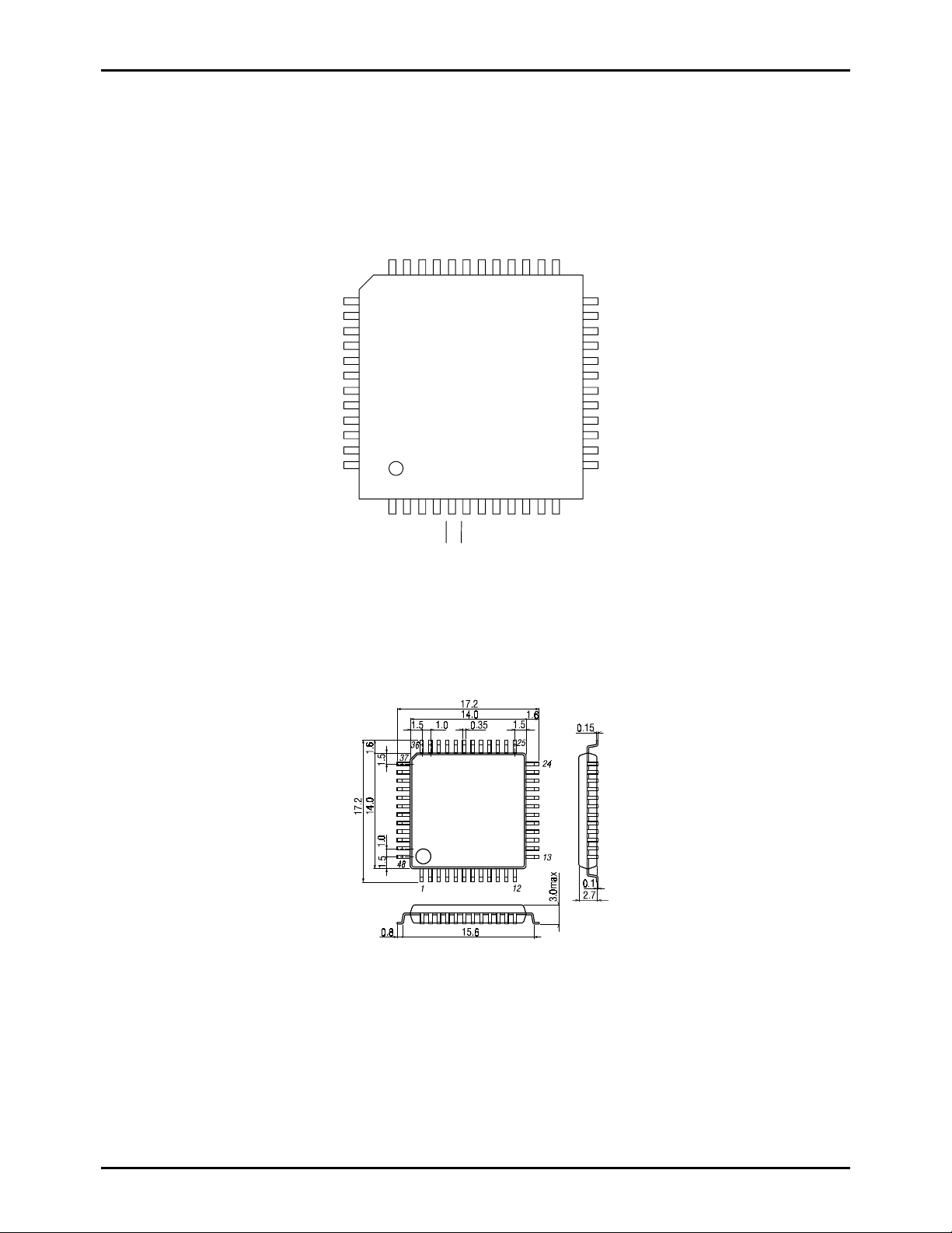
Pin Assignment
•QIP48E
Package Dimension
(unit : mm)
3156
P13/SO1
P14/SI1/SB1
P15/SCK1
P16/BUZ
P17/PWM0
NC
P00
P01
P02
P03
P04
NC
LC865520B/16B/12B/08B/04B
P12/SCK0
P11/SI0/SB0
P10/SO0
P36
P35
P34
P33
NC
P32
P31
P30
3635343332313029282726
37
38
39
40
41
42
43
44
45
46
47
48
1 2 3 4 5 6 7 8 9
P05
P06
P07
RES
XT1/P74NCXT2/P75
P70/INT0
10
11
CF1
CF2
VSS
P73/INT3/T0IN
25
24
23
22
21
20
19
18
17
16
15
14
13
12
VDD
NC
P72/INT2/T0IN
P71/INT1
P87/AN7
P86/AN6
P85/AN5
NC
P84/AN4
P83/AN3
P82/AN2
P81/AN1
P80/AN0
*Leave NC pins open.
SANYO : QIP-48E
No.6697-6/21
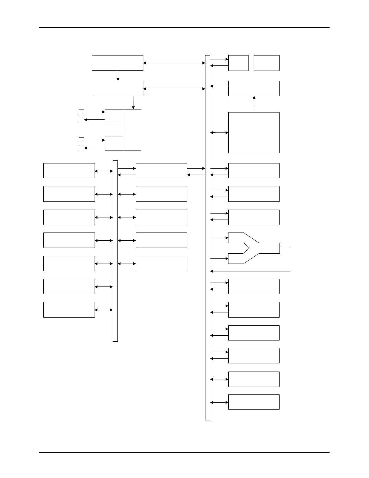
System Bl ock Diagram
SIO0
Timer 1
ADC
INT0-3
Noise Rejection Filter
Interrupt Control
Stand-by C ontr ol
X’tal
CR
RC
LC865520B/16B/12B/08B/04B
Clock
Generator
Port 1
Port 7 SIO1
Port 8 Timer 0
Port 3
PLA IR
ROM
PC
ACC Bus Interface Base Timer
B Register
C Register
ALU
PSW
RAR
RAM
Stack Pointer
Port 0
Watch Do g Timer
No.6697-7/21
 Loading...