

Overview
The LC8213K compresses and expands the binary image
data used in fax and similar applications and can be used
in office automation equipment such as G3 or G4
facsimile systems, image filing systems, digital copiers,
and engineering workstations. The LC8213K supports
encoding methods that conform to the MH (Modified
Huffman), MR (Modified relative element address
designate), and MMR (Modified MR) encoding
techniques as stipulated in the ITU-T T.4 and T.6
recommendations.
Features
• Conforms to the ITU-T T.4 and T.6 MH, MR, and
MMR encoding methods.
• Supports G3 and G4 facsimile.
• Handles up to 64k bits in the main scan direction.
• Line skip mode
• 8/16-bit image memory bus, 8-bit CPU bus
• Supports data transfers between the CPU bus and the
image memory bus.
• DMA transfer function for data transfers between image
memory and I/O devices
• Executes encoding processing and DMA transfers
simultaneously
• System clock frequency: Up to 25 MHz
• CMOS structure supporting low power dissipation
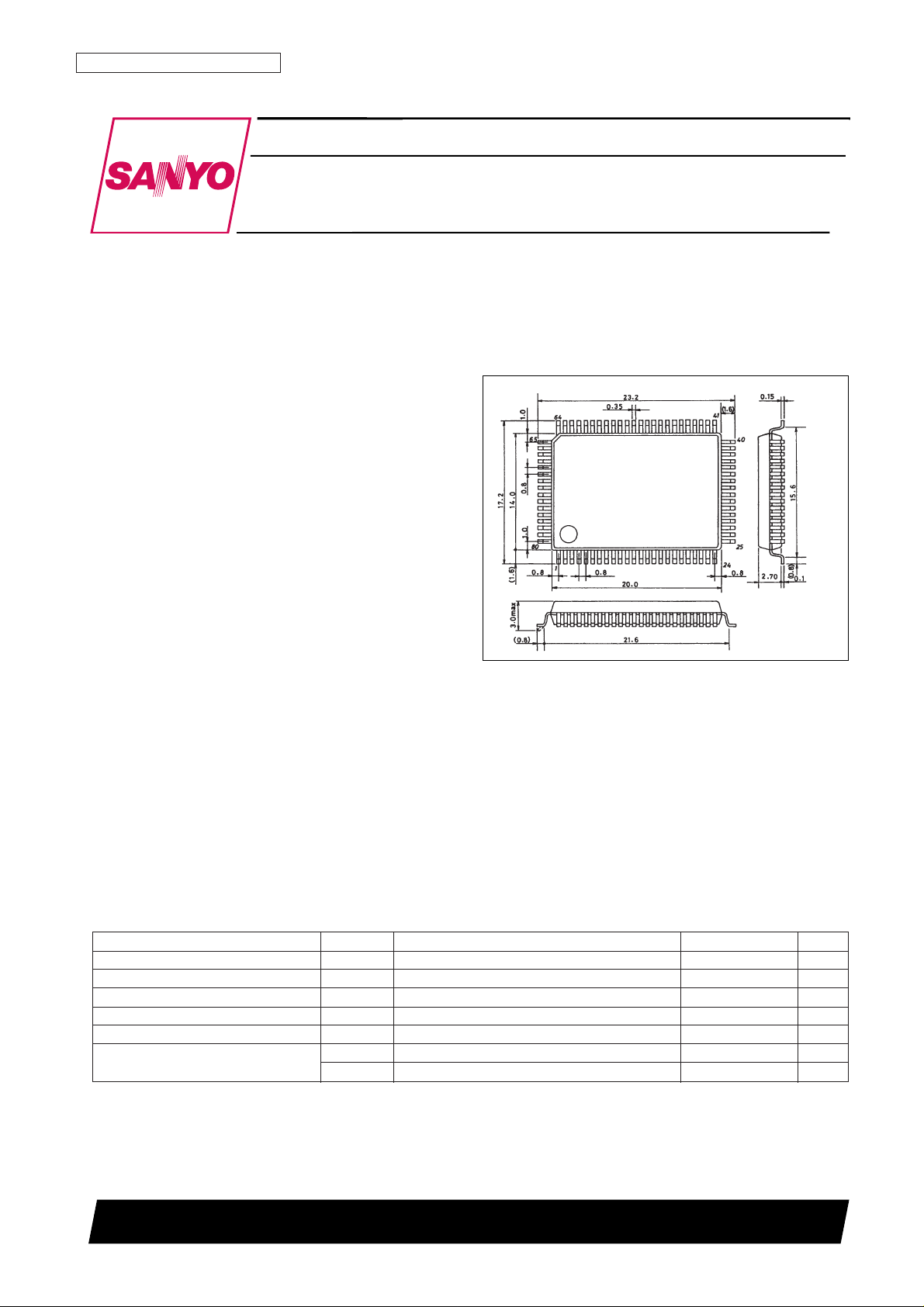
Package Dimensions
unit: mm
3174-QFP80E
CMOS LSI
Ordering number : EN *5753
93097HA (OT) No. 5753-1/5
Preliminary
SANYO Electric Co.,Ltd. Semiconductor Bussiness Headquarters
TOKYO OFFICE Tokyo Bldg., 1-10, 1 Chome, Ueno, Taito-ku, TOKYO, 110 JAPAN
Image Data Compression/Expansion Processor
LC8213K
Specifications
Absolute Maximum Ratings at Ta = 25°C, VSS= 0 V
Parameter Symbol Condition Ratings Unit
Maximum supply voltage V
DD
max –0.3 to +7.0 V
Input and output voltages V
I
, V
O
–0.3 to VDD+ 0.3 V
Allowable power dissipation Pd max Ta ≤ 70°C 500 mW
Operating temperature Topr –30 to +70 °C
Storage temperature Tstg –55 to +125 °C
Soldering conditions
Hand soldering: 3 seconds 350 °C
Reflow soldering: 10 seconds 235 °C
[LC8213K]
SANYO: QIP80E
Allowable Operating Ranges at Ta = –30 to +70°C, VSS= 0 V
DC Characteristics at Ta = –30 to +70°C, VDD= 4.5 to 5.5 V
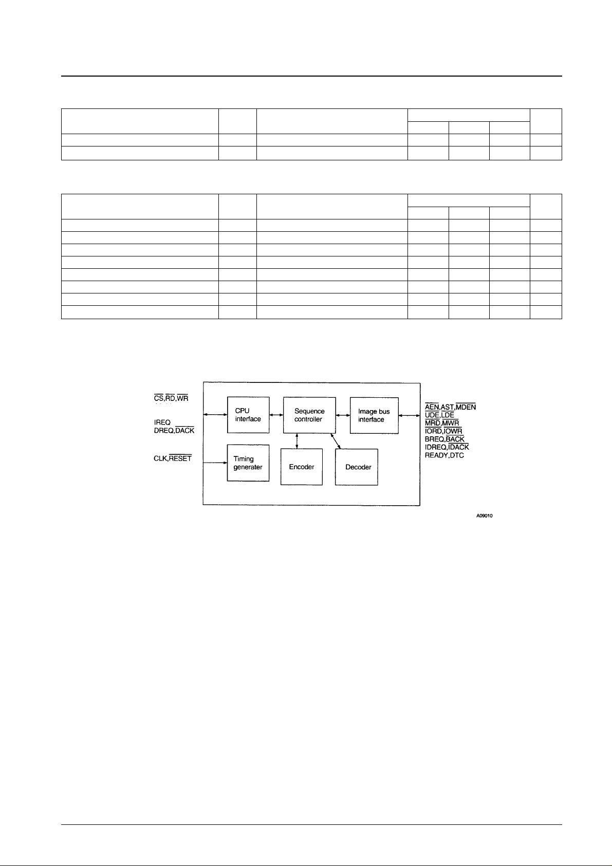
Block Diagram
• CPU interface
This circuit is a general-purpose 8-bit CPU interface. The operating mode and other aspects are set by accessing the
interface registers and the parameter registers.
• Sequence controller
Controls the functional blocks in the IC according to the encoding or decoding algorithm being used.
• Encoder
Generates the codes in the various modes by recognizing inflection points in the image data. Encoded data is passed to
the data bus through an 8-bit 4-word encoding FIFO (EFIFO).
• Decoder
Recognizes the codes in the various modes and recovers the original image data. Image data is passed to the data bus
through a decoding FIFO (DFIFO).
• Image bus interface
Controls reads from and writes to image memory as well as DMA transfers on the image memory bus.
No. 5753-2/5
LC8213K
Parameter Symbol Conditions
Ratings
Unit
min typ max
Supply voltage V
DD
4.5 5.0 5.5 V
Input voltage range V
IN
0 V
DD
V
Parameter Symbol Conditions
Ratings
Unit
min typ max
Input high-level voltage V
IH
1 2.2 V
Input low-level voltage V
IL
1 0.8 V
Input leakage current I
L
–10 +10 µA
Output high-level voltage V
OHIOH
= –4 mA 2.4 V
Output low-level voltage V
OLIOL
= 4 mA 0.4 V
Output leakage current I
OZ
For pins in the high-impedance output state –10 +10 µA
Input clock frequency f
CLK
CLK 25 MHz
Current drain I
DD
10 20 mA
A2 to A0
D7 to D0
TEST4 to TEST0
MA23 to MA16
MA/MD15 to MA/MD0
 Loading...