

Overview
The LC82103 converts the analog video signal from the
CCD contact image sensor into high-precision binary
image data. The LC82103 includes an 8-bit A/D converter
and two 6-bit D/A converters. The 6-bit D/A converters
are used for setting reference potential (high and low) of
the 8-bit A/D converter. The LC82103 converts the input
analog data to high precision multilevel data, that is
produced by all pixel shading correction process, multilevel image resolution converting process, and γ
correction process of user defined curves. That multilevel
data is converted to high-precision bi-level image that is
produced by using two dimensional filtering, a image
separation method, and an error diffusion technique.
Finally the LC82103 is able to reduce the image in the
horizontal and vertical directions, too. The LC82103
requires absolutely no external memory since it limits the
number of pixels processed to 3072/line. This LSI can
implement the image processing used by FAX, copier, and
OCR applications.
Features
• Number of pixels processed: 3072 pixels/line
• Processing speed: 250 ns/pixel maximum (When
CLKIN = 32 MHz)
• Built-in 8-bit A/D converter (with a sensor signal timing
adjustment function)
• Built-in two 6-bit D/A converters for setting the A/D
converter high and low reference potential
• Sensor drive circuit (supports CCDs and several CIS
types)
• Digital clamping (single-point clamping, even/odd
clamping)
• Distortion correction (white correction: all pixels, black
correction: settable black correction subtracted data)
• γ correction (support user-defined curves: 8-bit data)
• Image area separation (characters, photographs,
screened halftone areas)
• Simple binary coding process (fixed threshold,
brightness adaptive threshold)
• Intermediate processing error diffusion (64 levels)
• Multilevel image resolution conversion (1/2, 2/3, 3/2,
2/1)
• Binary image reduction (horizontal: thinning, fine black
line retaining, fine white line retaining, vertical:
thinning, fine black line retaining)
• Single-voltage 5 V supply and low power due to CMOS
process fabrication
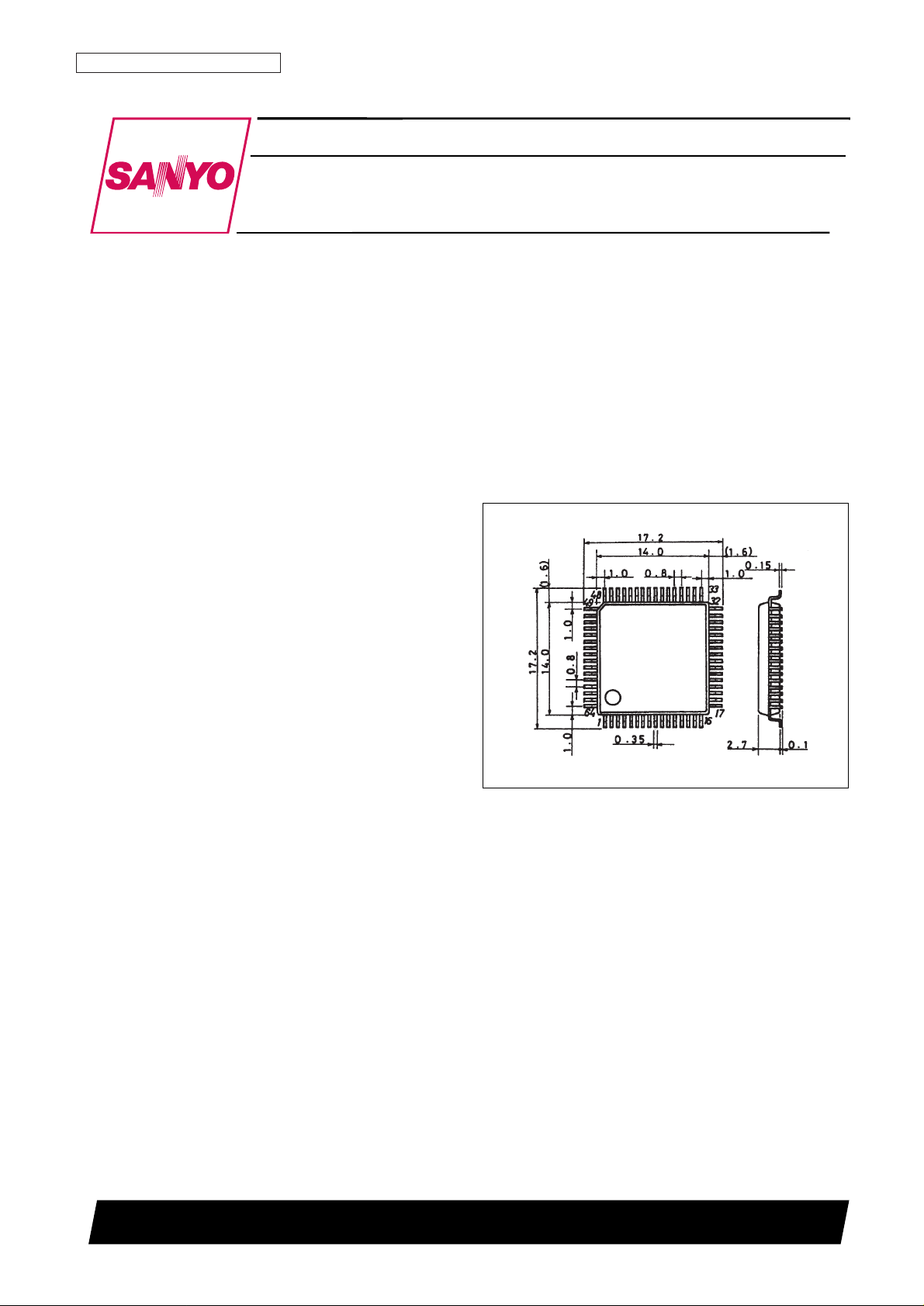
Package Dimensions
unit: mm
3159-QFP64E
CMOS LSI
63096HA (OT) No. 5402-1/5
Preliminaly
SANYO: QFP64E
[LC82103]
SANYO Electric Co.,Ltd. Semiconductor Bussiness Headquarters
TOKYO OFFICE Tokyo Bldg., 1-10, 1 Chome, Ueno, Taito-ku, TOKYO, 110 JAPAN
Image-Processing LSI for Facsimile, Copier,
and OCR Applications
LC82103
Ordering number : EN*5402

No. 5402-2/5
LC82103
Parameter Symbol Conditions Ratings Unit
Maximum supply voltage V
DD
max –0.3 to +7.0 V
Maximum input and output voltages V
I
, VOmax –0.3 to VDD+ 0.3 V
Allowable power dissipation Pd max Ta ≤ 70°C 350 mW
Operating temperature Topr –30 to +70 °C
Storage temperature Tstg –55 to +125 °C
Soldering temperature endurance
Hand soldering: 3 seconds 350 °C
Reflow soldering: 10 seconds 235 °C
Specifications
Absolute Maximum Ratings at Ta = 25°C, GND = 0 V
Parameter Symbol Conditions
Ratings
Unit
min typ max
Supply voltage V
DD
4.5 5.5 V
Input voltage V
IN
0 V
DD
V
Allowable Operating Ranges at Ta = –30 to +70°C, GND = 0 V
Parameter Symbol Conditions
Ratings
Unit
min typ max
Input high-level voltage V
IH
2.2 V
Input low-level voltage V
IL
0.8 V
Input leakage current I
IH, LVIN
= VDD, V
SS
–10 +10 µA
Output high-level voltage V
OHIOH
= –3 mA 2.4 V
Output low-level voltage V
OLIOL
= 3 mA 0.4 V
Output leakage current I
OZ
At high impedance –10 +10 µA
Current drain I
DD
CLKIN = 32 MHz 40 70 mA
DC Characteristics at Ta = –30 to +70°C, GND = 0 V, VDD= 4.5 to 5.5 V
Parameter Symbol Conditions min typ max Unit
[D/A Converter]
Resolution 6 bit
Internal resistance 4.8 kΩ
[A/D Converter] When the ATAPL potential = 0.8 V, ATAPH potential = 4.2 V
Resolution 8 bit
Linearity error ±1 LSB
Differential linearity error ±1 LSB
Internal resistance 330 Ω
Analog Characteristics
 Loading...