

SANYO LC82101 Datasheet
CMOS LSI
Ordering number : EN*4982A
63095HA (OT) No. 4982-1/5
Preliminary
SANYO Electric Co.,Ltd. Semiconductor Bussiness Headquarters
TOKYO OFFICE Tokyo Bldg., 1-10, 1 Chome, Ueno, Taito-ku, TOKYO, 110-8534 JAPAN
Image Processing Circuit
for FAX, Copier, and OCR Products
LC82101
Overview
The LC82101 converts an analog image signal from a
CCD or contact sensor to high-quality binary image data.
The LC82101 uses an internal 8-bit A/D converter for
A/D conversion, and in addition to the orthodox dithering
technique, also supports an error diffusion technique that
allows an even higher quality image to be acquired. These
techniques apply to the whole range of processing
supported by the LC82101, including full-pixel distortion
correction, gamma conversion for arbitrary gamma
curves, image compression processing, two-dimensional
filtering, halftone processing, and image separation
processing to separate documents into text, photograph,
and halftone regions. Thus this LSI implements the image
processing required by FAX, copier, and OCR systems.
Features
• Number of pixels processed
2048 pixels/line (64 KB memory, white correction only)
4096 pixels/line (256 KB memory, both white and black
correction)
8192 pixels/line (256 KB memory, white correction
only)
• Processing speed
500 ns/pixel maximum (The processing time for 1 pixel
is 16/SYSCLK.)
• Supports medium speed products with a single external
memory chip
100 ns access time memory allows 800 ns/pixel
processing, and 60 ns access time memory allows
500 ns/pixel processing.
• AGC (The A/D converter high-level reference voltage is
varied from 1.2 to 4.2 V in 0.2 V steps.)
• Built-in 8-bit A/D converter (includes a sensor signal
delay adjustment function)
• Sensor drive circuit (supports CCD and all CIS types)
• Digital clamp (single-point clamp, even/odd clamp)
• Distortion correction (white correction, black correction,
full-pixel correction)
• Gamma correction (supports user-defined curves)
• Image area separation (text, photographs, halftone)
• Simple binary-conversion processing (fixed threshold
level, density-adaptive threshold level)
• Halftone processing
Structural dithering (64 levels), settable dithering
threshold level
Error diffusion technique (64 levels)
• Image reduction (thinning, fine black line retaining, fine
white line retaining)
• Single-voltage 5 V supply and low power due to CMOS
process fabrication
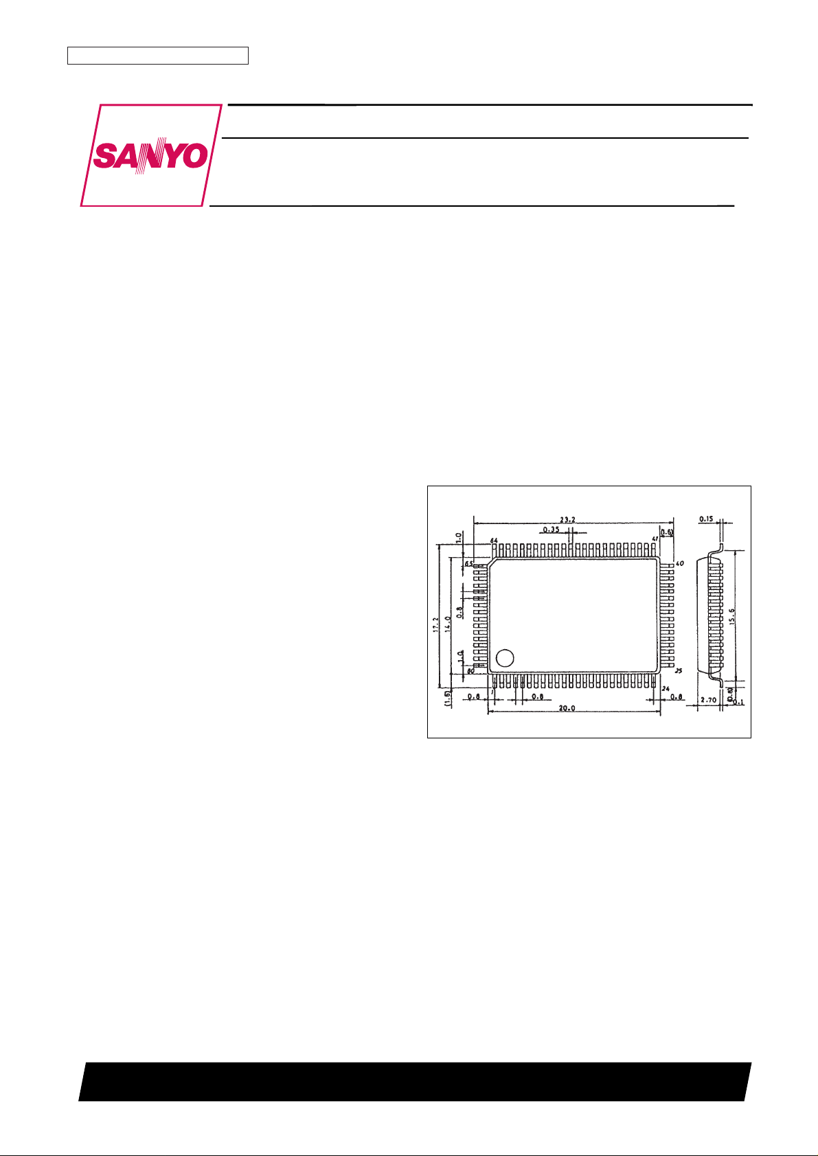
Package Dimensions
unit: mm
3174-QFP80E
SANYO: QIP80E
[LC82101]

Block Diagram
Pin Functions
Type: I: Input pin, O: Output pin, B: Bidirectional pin, P: Power supply pin, NC: No connection
No. 4982-2/5
LC82101
Pin No. Symbol I/O Function
1 DREQ O DMA data request signal output
2 ACK I DMA acknowledge signal input
3 PD0 O
4 PD1 O Binary image data parallel data bus
5 PD2 O The data order is set by the MSBF register.
6 PD3 O
7 PD4 O
8 PD5/SDE O Pin 8 can be switched to function as the serial data output valid period signal.
9 PD6/SDCK O Pin 9 can be switched to function as the serial data transfer clock.
10 PD7/SD O Pin 10 can be switched to function as the serial data output.
11 MD0 B External memory data bus
12 DV
DD
P Digital system power supply
13 DGND P Digital system ground
14 MD1 B
15 MD2 B
16 MD3 B
External memory data bus
17 MD4 B
MD7 is the MSB and MD0 is the LSB.
18 MD5 B
19 MD6 B
20 MD7 B
21 DGND P Digital system ground
22 MA0 O
23 MA1 O
24 MA2 O
25 MA3 O
External memory address
26 MA4 O
MA14 is the MSB and MA0 is the LSB.
27 MA5 O
28 MA6 O
29 MA7 O
30 MA8 O
Continued on next page.
 Loading...