Overview
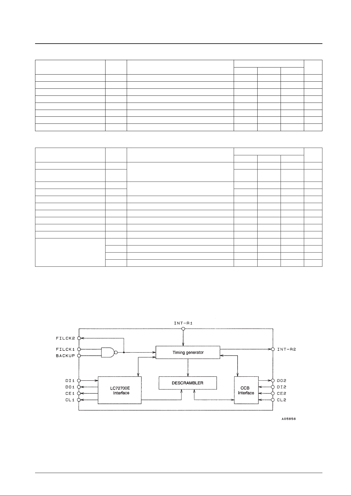
The LC80101M is a special-purpose descrambler LSI for
use in VICS systems. FM multiplexed service data that
has had VICS center scrambling applied can be
descrambled and received by inserting this LSI in the
serial interface between the LC72700E and the application
CPU. This architecture also supports reception of regular
transmissions that have not been scrambled. Note that
sample evaluation and product manufacture using this LSI
require a contract with the VICS Center organization.
Functions
• VICS scrambled/unscrambled recognition circuit
• Dedicated VICS descrambler circuit
• CPU interface circuit (CCB: serial)
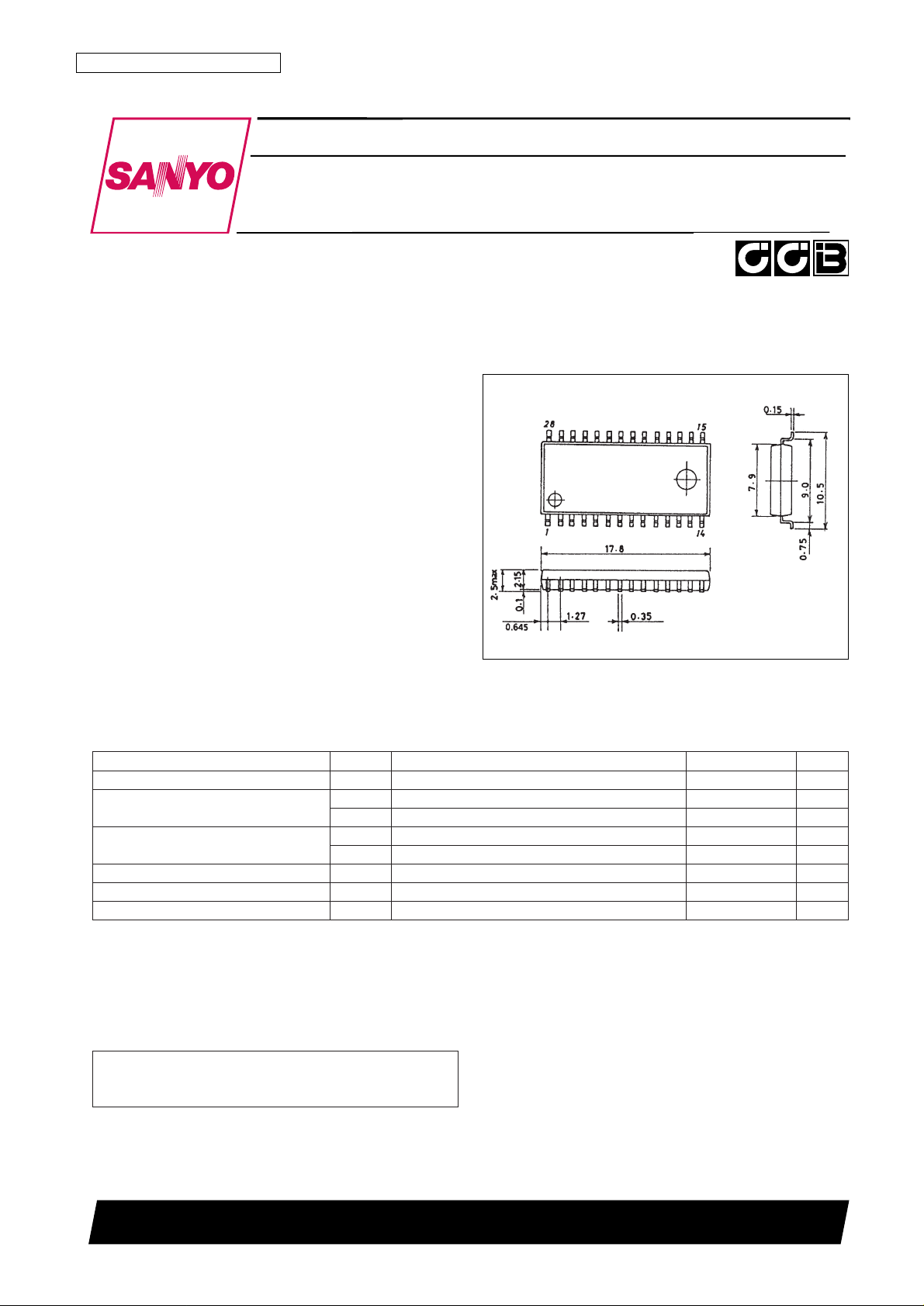
Package Dimensions
unit: mm
3091A-MFP28
CMOS LSI
53096HA (OT) No. 5438-1/9
SANYO: MFP28
[LC80101M]
SANYO Electric Co.,Ltd. Semiconductor Bussiness Headquarters
TOKYO OFFICE Tokyo Bldg., 1-10, 1 Chome, Ueno, Taito-ku, TOKYO, 110 JAPAN
VICS LSI
LC80101M
Ordering number : EN54384465
Parameter Symbol Conditions Ratings Unit
Maximum supply voltage V
DD
max V
DD
–0.3 to +7.0 V
Input voltage
V
IN
1 The CL2, CE2, DI2, RST2, BACKUP, INT-R1, and DI1 pins –0.3 to +7.0 V
V
IN
2 Input pins other than VIN1 –0.3 to VDD+0.3 V
Output voltage
V
OUT
1 The DO2 pin –0.3 to +7.0 V
V
OUT
2 Output pins other than V
OUT
1 –0.3 to VDD+0.3 V
Allowable power dissipation Pdmax Ta ≤ 85
°C 200 mW
Operating temperature Topr –40 to +85 °C
Storage temperature Tstg –55 to +125 °C
Specifications
Absolute Maximum Ratings
• CCB is a trademark of SANYO ELECTRIC CO., LTD.
• CCB is SANYO’s original bus format and all the bus
addresses are controlled by SANYO.

No. 5438-2/9
LC80101M
Parameter Symbol Conditions
Ratings
Unit
min typ max
Clock low-level time t
CL
CL2 0.7 µs
Clock high-level time t
CH
CL2 0.7 µs
Data setup time t
SU
CL2, DI2 0.7 µs
Data hold time t
HD
CL2, DI2 0.7 µs
CE wait time t
EL
CL2, CE2 0.7 µs
CE setup time t
ES
CL2, CE2 0.7 µs
CE hold time t
EH
CL2, CE2 0.7 µs
Data output time t
DH
DO2: Varies with the value of the pull-up resistor used 1 µs
Serial Input and Output (See the serial data timing figures.)
Parameter Symbol Conditions
Ratings
Unit
min typ max
Input high-level voltage V
IH
CMOS-compatible Schmitt inputs 0.8 V
DD
V
Input low-level voltage V
IL
Pull-down resistors: INT-R1, TEST1 to TEST4,
0.2 V
DD
V
and TESTON
Input high-level voltage V
IH
CMOS-compatible Schmitt inputs: 0.8 V
DD
V
Input low-level voltage V
IL
BACKUP, CE2, CL2, DI1, DI2, and RST2
0.2 V
DD
V
Output high-level voltage V
OHIOH
= –4 mA: CE1, CL1, DO1, INT-R2 VDD– 2.1 V
Output low-level voltage V
OLIOL
= 4 mA: CE1, CL1, DO1, INT-R2 0.4 V
Output low-level voltage V
OLIOL
= 2 mA: DO2 0.4 V
Standby current Isd With the BACKUP pin low 0.01 10 µA
Input sensitivity Vck Rf = 1 MΩ, FILCK1 = 3.6 MHz: FILCK1*
1
1.0 V
DD
Vp-p
Pull-down resistance Rd INT-R1, TEST1 to 4, TESTON 70 140 280 kΩ
I
DD
1 Sine wave input: 1 V p-p, VDD= 5.0 V*
2
6 15 mA
Current drain
I
DD
2 Sine wave input: 5 V p-p, VDD= 5.0 V*
2
2.5 7 mA
I
DD
3 Square wave input: 1 V p-p, VDD= 5.0 V*
2
5 13 mA
I
DD
4 Square wave input: 5 V p-p, VDD= 5.0 V*
2
1.5 4 mA
Electrical Characteristics/Input and Output Levels at Ta = –40 to +85°C, VDD= 4.5 to 5.5 V, VSS= 0 V
Note 1. Since this LSI operates based on the rising edge of the LC72700E 3.6 MHz output (the FILCK pin), the LC72700E 3.6 MHz output signal must be
input to the FILCK1 pin without inverting the polarity.
2. The current drain varies with the input level and the shape of the clock signal input to the FILCK1 pin. The current drain can be reduced by using
waveforms that are closer to square waves than to sine waves, and by using a signal level that is close to V
DD
. The LC72700E 3.6 MHz output is a
square wave with an output level equal to V
DD
.
Block Diagram

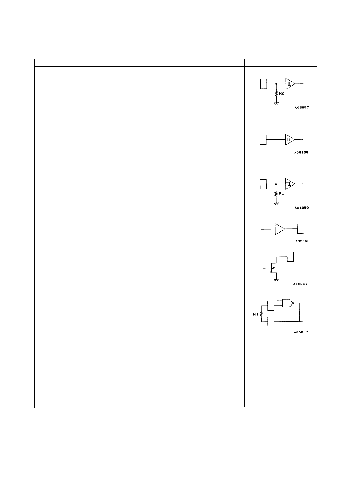
Pin Assignments and Functions
No. 5438-3/9
LC80101M
Pin No. Pin Function overview Input or output circuit type
1
9
19
27
13
TEST1
TEST2
TEST3
TEST4
TESTON
Test pin 1 (Must be connected to ground or left open in normal operation.)
Test pin 2 (Must be connected to ground or left open in normal operation.)
Test pin 3 (Must be connected to ground or left open in normal operation.)
Test pin 4 (Must be connected to ground or left open in normal operation.)
Test pin (Must be connected to ground in normal operation.)
Rd: Input pin internal pull-down resistor
4 INT-R1
Inputs the output of the LC72700E pin 35.
Rd: Input pin internal pull-down resistor
5
20
21
22
23
26
DI1
BACKUP
CL2
CE2
DI2
RST2
Inputs the output of the LC72700E pin 32. An external pull-down resistor is
required. See the following page.
Input that selects normal operation when high and backup mode when low.
Clock input for the CCB serial interface
Control input for the CCB serial interface
Data input for the CCB serial interface
System reset input (negative logic)
6
7
8
25
DO1
CE1
CL1
INT-R2
Output to the LC72700E pin 31 input
Output to the LC72700E pin 30 input
Output to the LC72700E pin 29 input
Outputs an output data interrupt to the external CPU
2
3
FILCK1
FICLK2
System clock generator input
System clock generator output
Rf: External feedback resistor, 510 kΩ to 1.5 MΩ (typical: 1 MΩ)
28
14
V
DD
V
SS
Power supply (+4.5 to 5.5 V)
Ground connection
10, 11,
12, 15,
16, 17
18
NC No connection pins. These pins must be left open.
24 DO2 Data output for the CCB serial interface
 Loading...