

SANYO LC7930NW, LC7930N Datasheet
Ordering number: EN2778C
CMOS LSI
LC7930N, 7930NW
LCD Drivers
Overview
The LC7930N, 7930NW are CMOS LSIs which incorporate
20-bit shift register, latch, and two sets of 20 LCD drivers.
They also have two switching pins: one of them (channel 2)
can be used as a scan-line driver (back plate) and the other
(channel 1) as a segment driver. They are optimal for LCD
interface with microcontroller (4 or 8 bits) or dot matrix
controller circuit incorporating character generator.
Features
.
Two channels of 20 output segment drivers
.
The configuration of 20 output segment drivers + 20
scanning terminal drivers available
.
A series data to connect with the microcontroller and three
control signals
.
Able to be connected in series for large display
.
Built-in bidirectional shift register can be shifted in the
direction that makes wiring easy
.
Operating supply voltage/ Operating temperature:
V
= 4.5 to 5.5 V / Topr = –20 to +75°C
DD
.
Operating current drain : IDD= 1.0 mA max
(Logic = 400 kHz, LCD = 1 kHz)
.
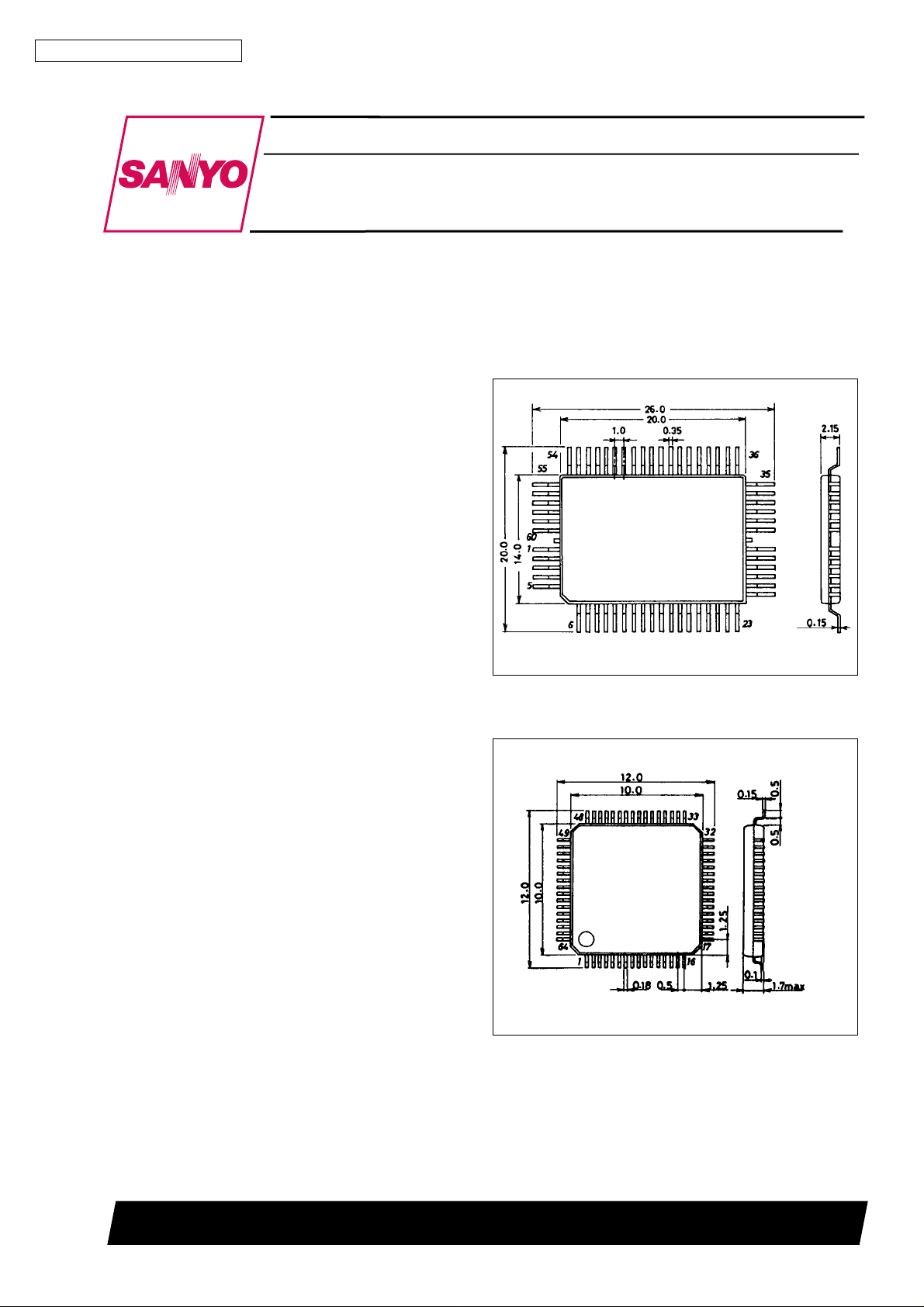
Package : Pin 60 Flat LC7930N : QIP60
Pin 64 Flat LC7930NW : SQFP64
Package Dimensions
unit : mm
3055A-QFP60C
[LC7930N]
SANYO : QIP60C
unit : mm
3190-SQFP64
[LC7930NW]
SANYO : SQFP64
SANYO Electric Co.,Ltd. Semiconductor Bussiness Headquarters
TOKYO OFFICE Tokyo Bldg., 1-10, 1 Chome, Ueno, Taito-ku, TOKYO, 110 JAPAN
13097HA(II)/12593JN/6031JN/6218TA,TS No.2778-1/7
LC7930N, 7930NW
Specifications
Absolute Maximum Ratings atTa=25±2°C
Parameter Symbol Conditions Ratings Unit
V
max –0.3 to +7.0 V
t
t
DD
CL
SU
SL
LS
ct
DH
DD
V
max VDD–13.5 to VDD+0.3 V
EE
max
I
max
O
V
DD
Note (1) 0.7V
IH
Note (1) V
IL
CLK
CLKSR, CLK
CLK
V1, V2, V3, V4, V5, V6 V
Output transistor OFF, Y1 to Y40 V
SR
LA
SR
LDATA1, LDATA2,
RDATA1, RDATA2
CLKSR, CLK
CLKSR, CLK
CLKSR, CLK
LA
LA
LA
CLKSR→ CLK
CLKLA→ CLK
LA
SR
LDATA1, LDATA2,
RDATA1, RDATA2
–0.3 to V
EE
–0.3 to V
EE
+0.3 V
DD
to VDD+0.3 V
+0.3 V
DD
to VDD+0.3 V
4.5 5.5 V
DD
SS
0.3V
V
DD
DD
400 kHz
800 ns
800 ns
300 ns
500 ns
500 ns
200 ns
300 ns
Maximum supply voltage
Maximum input voltage V
Maximum output voltage V
Allowable power dissipation Pd max 100 mW
Operating temperature Topr –20 to +75 °C
Storage temperature Tstg –55 to +125 °C
Note : Don’t soak the whole of IC into the tank filled with melted solder for soldering
Allowable Operating Conditions at Ta = –20 to +75°C, VSS=0V,VEE=–4to–6V
Parameter Symbol Conditions min typ max Unit
Supply voltage V
High-level input voltage V
Low-level input voltage V
Shift frequency f
High-level clock width t
Low-level clock width t
Data setup time t
Clock setup time
Clock transition time t
Data retention time t
CWH
CWL
V
V
Electirical Characteristics at Ta = –20 to +75°C, VDD=+5V±10%, VSS=0V,VEE=–4to–6V
Parameter Symbol Conditions min typ max Unit
Input leakage current
I
I
High-level output voltage V
Low-level output voltage V
Vi to Yj voltage down
V
V
I
VH
Vi quiescent current
I
VL
I
DD
Supply current
I
EE
Output propagation
delay time
t
PD
Note (1): Applied to the pins; CLKSR, CLKLA, LDATA1, RDATA1, LDATA2, RDATA2, M, L/R1, L/R2, CH2-BP
(2): The equivalent circuit between Vi to Yj (i=1to6,j=1to40)
Note (1) Vin = V
IH
Note (1) Vin = V
IL
LDATA1, LDATA2,
OH
RDATA1, RDATA2
LDATA1, LDATA2,
OL
RDATA1, RDATA2
Y1 to Y40 Note (2) Ion = 100 µA, single output 1.1 V
d1
Y1 to Y40 Note (2) Ion = 50 µA, all outputs 1.5 V
d2
V1 to V6
V1 to V6
V
DD
V
EE
LDATA1, LDATA2,
RDATA1, RDATA2
DD
SS
I
= –0.4 mA VDD–0.4 V
OH
I
= 0.4 mA 0.4 V
OL
–5 µA
Open output pins
Vin=V
DD
Open output pins
Vin=V
EE
–10 µA
Open output pins
CLK
= 400 kHz
SR
Open output pins
M=1kHz
C
= 15 pF 500 ns
L
5µA
10 µA
1.0 mA
10 µA
No.2778-2/7
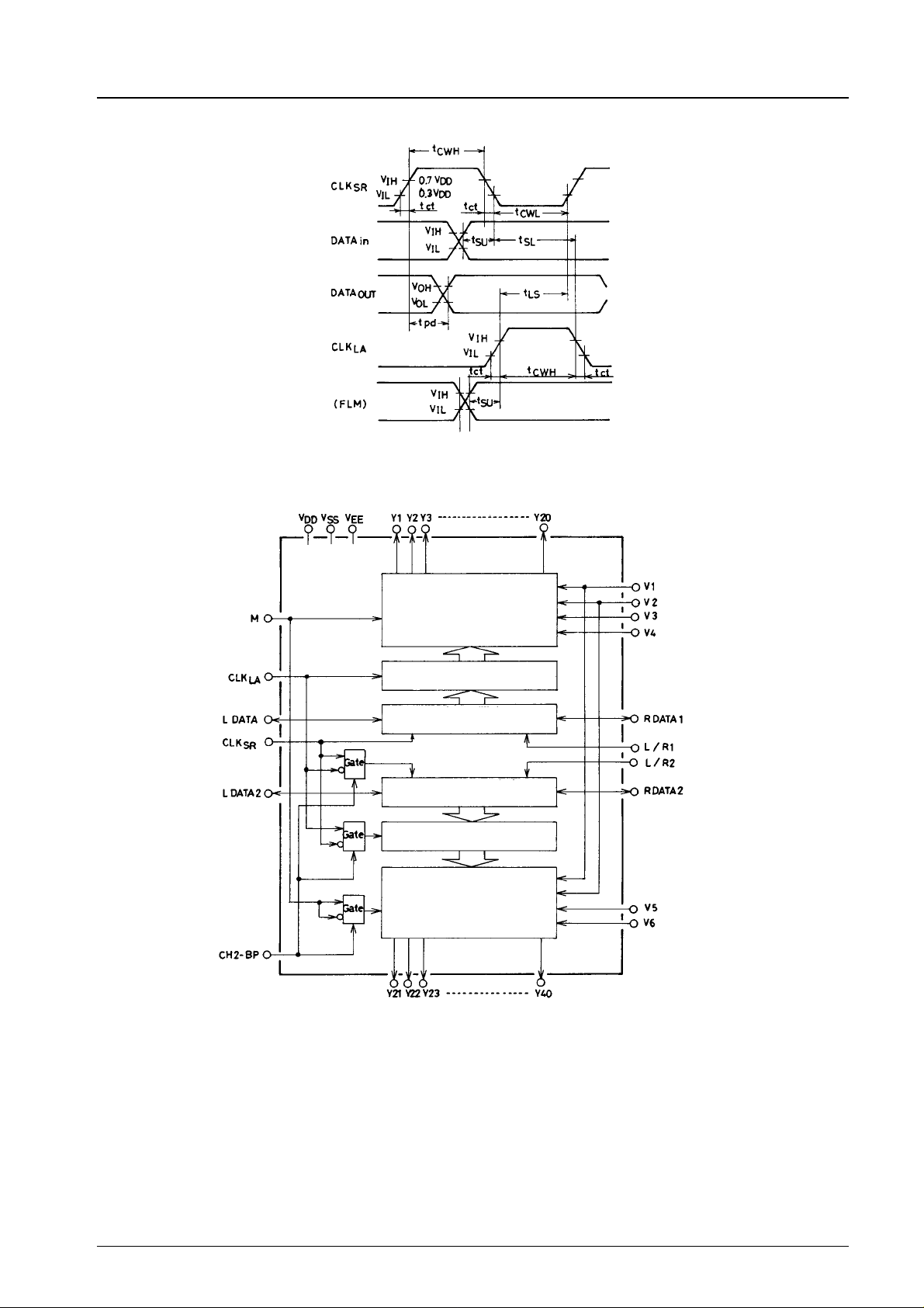
Switching Waveforms
Internal Equivalent Circuit
LC7930N, 7930NW
LCD driver
(Channel 1)
20-bit latch
20-bit bidirectional
shift register
20-bit bidirectional
shift register
20-bit latch
LCD driver
(Channel 2)
No.2778-3/7
 Loading...