

Page 1
Ordering number : EN*4450
O3098HA (OT)/92093JN No. 4450-1/7
LC78866V
SANYO Electric Co.,Ltd. Semiconductor Bussiness Headquarters
TOKYO OFFICE Tokyo Bldg., 1-10, 1 Chome, Ueno, Taito-ku, TOKYO, 110-8534 JAPAN
16-Bit A/D Converter
CMOS LSI
Any and all SANYO products described or contained herein do not have specifications that can handle
applications that require extremely high levels of reliability, such as life-support systems, aircraft’s
control systems, or other applications whose failure can be reasonably expected to result in serious
physical and/or material damage. Consult with your SANYO representative nearest you before using
any SANYO products described or contained herein in such applications.
SANYO assumes no responsibility for equipment failures that result from using products at values that
exceed, even momentarily, rated values (such as maximum ratings, operating condition ranges, or other
parameters) listed in products specifications of any and all SANYO products described or contained
herein.
Overview
The LC78866V is a 16-bit CMOS A/D converter with a
built-in 4-channel input multiplexer. The LC78866V is
optimal for use in low band digital sampling and uses a
charge redistribution successive approximation method as
its conversion technique.
Features
• A/D converter for use with 16-bit interface
microprocessors
• Charge redistribution successive approximation
conversion
• Built-in 4-channel input multiplexer
• LSB first, offset binary code output
• Built-in sample and hold circuit
• +5 V single voltage power supply
• Low power mode
• Miniature package (SSOP30)
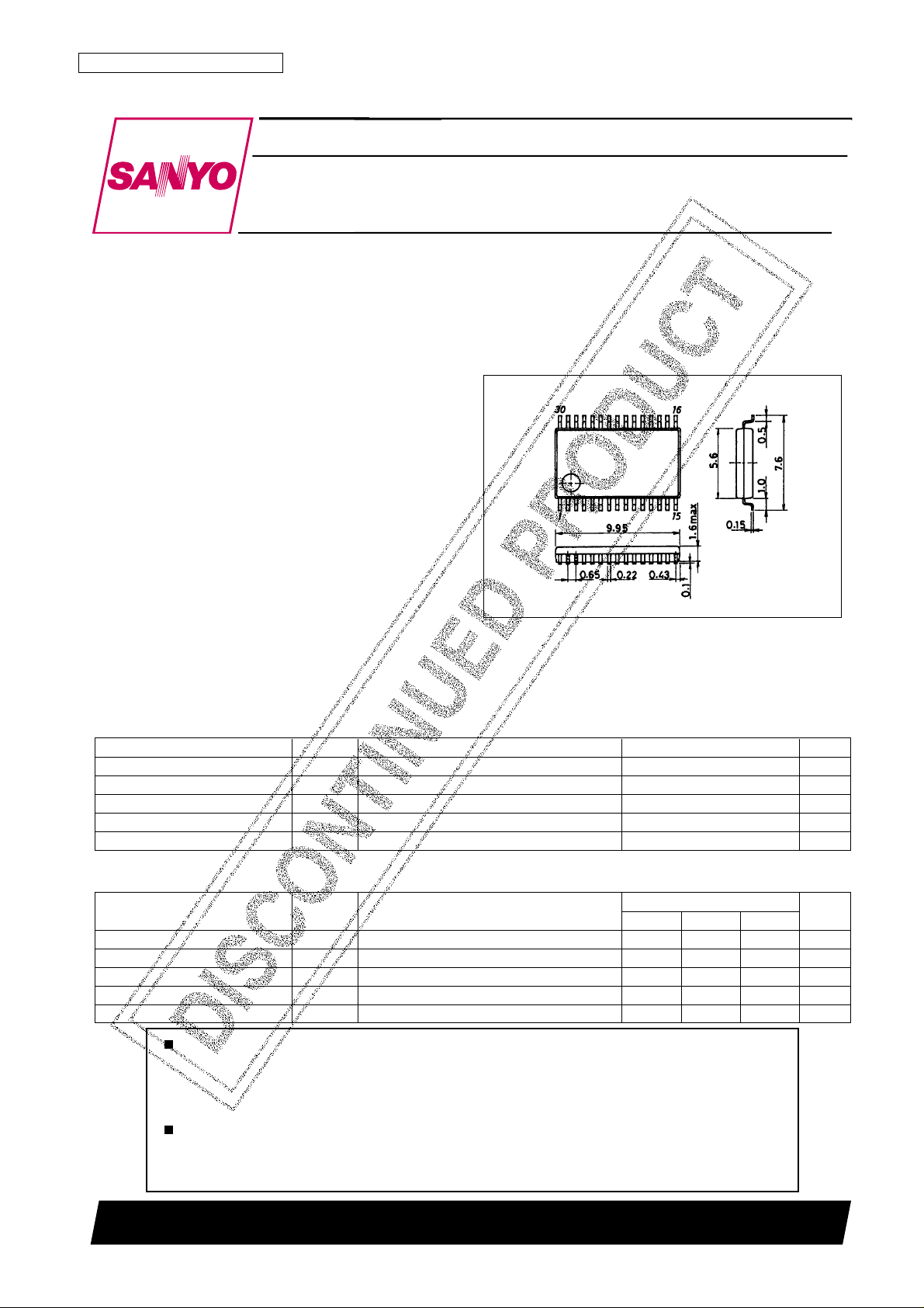
Package Dimensions
unit: mm
3191-SSOP30
Specifications
Absolute Maximum Ratings at Ta = 25°C, VSS= 0 V
Allowable Operating Ranges
Parameter Symbol Conditions Ratings Unit
Maximum supply voltage V
DD
max –0.3 to +7.0 V
Maximum input voltage V
IN
max –0.3 to VDD+ 0.3 V
Maximum output voltage V
OUT
max –0.3 to VDD+ 0.3 V
Operating temperature Topr –20 to +75 °C
Storage temperature Tstg –40 to +125 °C
Parameter Symbol Conditions
Ratings
Unit
min typ max
Supply voltage V
DD
4.5 5.0 5.5 V
Reference voltage (high level) V
H
3.3 V
DD
V
Reference voltage (low level) V
L
0 1.2 V
Analog input voltage V
AIN
V
L
V
H
V
Operating temperature Topr –20 +75 °C
[LC78866V]
SANYO: SSOP30
Page 2
DC Electrical Characteristics at Ta = –20 to +75°C, VDD= 4.5 to 5.5 V, VSS= 0 V
Note: Digital input pins other than SCK.
AC Electrical Characteristics at Ta = –20 to +75°C, VDD= 4.5 to 5.5 V, VSS= 0 V
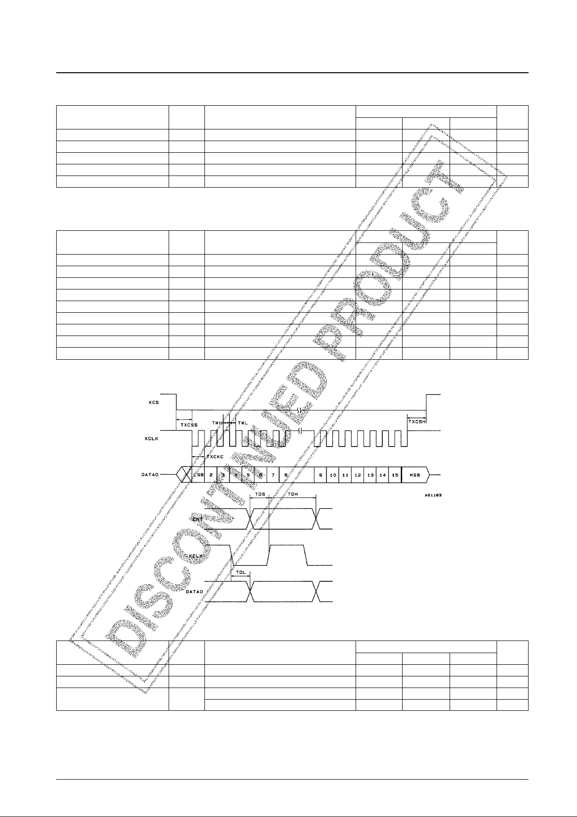
Timing Diagram
Analog Characteristics at Ta = 25°C, AV
DD
= DVDD= 5.0 V, VL= 0 V
Note: The A/D converter performs one conversion every F
SCK
/288 period and loads the converted data into the output register in a single operation.
Therefore, when XCS is high, the output register is continually updated every 288 SCK clock cycles, and at the point XCS goes low, data update is
stopped and data output preparation is performed.
No. 4450-2/7
LC78866V
Parameter Symbol Conditions
Ratings
Unit
min typ max
Input high level voltage (note) 2.2 V
Input low level voltage (note) 0.8 V
Output high level voltage I
OH
= –1 µA VDD– 0.05 V
Output low level voltage I
OL
= 1 µA VSS+ 0.05 V
Clock input amplitude SCK pin 0.5 V
P-P
Parameter Symbol Conditions
Ratings
Unit
min typ max
A/D conversion frequency fs (note) 17.4 49.7 55.6 kHz
Linearity error LE (note) 0.025 %
Power dissipation Pd
Normal mode 50 80 mW
Standby mode 15 30 mW
Parameter Symbol Conditions
Ratings
Unit
min typ max
XCS setup time T
XCSS
1.5 µs
XCS hold time T
XCSH
1.5 µs
XCLK cycle time T
XCKC
1.0 µs
XCLK pulse width T
WH
300 ns
XCLK pulse width T
WL
300 ns
CNT setup time T
DS
50 ns
CNT hold time T
DH
50 ns
DATAO delay time T
DL
0 150 ns
SCK clock frequency F
SCK
5 14.32 16 MHz
Page 3
Input Impedance at AVDD= DVDD= 5.0 V, VH= 5.0 V, VL= 0 V
Note: * Sampling frequency: 49.7 kHz
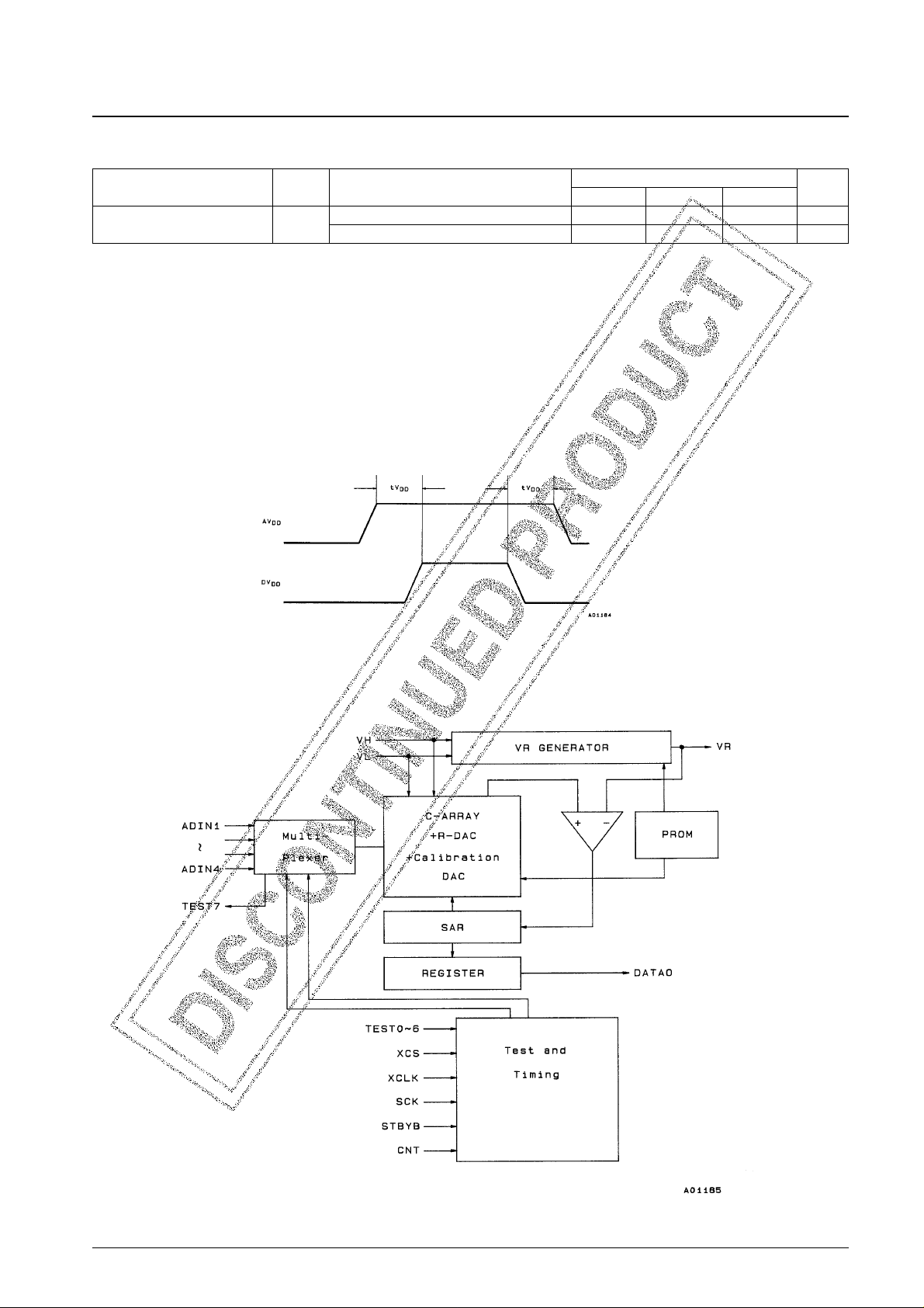
Power On Timing
AVDDand DVDDare completely independent.
AGND and DGND are connected through the IC substrate.
The optimal power on/off timing is to bring up (or down) the analog power supply (AV
DD
) and the digital power supply
(DV
DD
) voltages at the same time. If a time difference must be used, apply power first to the analog system and then to
the digital system, with a time difference (tV
DD
) of 2 to 3 ms or less. Power down the chip in the opposite order.
Block Diagram
No. 4450-3/7
LC78866V
Parameter Symbol Conditions
Ratings
Unit
min typ max
Input impedance A
DIN
DC input* 5 M Ω
AC 1 kHz input* 250 k Ω
Page 4

Pin Assignment
Pin Functions
No. 4450-4/7
LC78866V
Pin No. Pin Function and operating description
1 ADIN1 Analog input 1
2 NC No connection
3 ADIN2 Analog input 2
4 NC No connection
5 ADIN3 Analog input 3
6 NC No connection
7 ADIN4 Analog input 4
8 NC No connection
9 TEST7 Test output. Normally left open.
10 NC No connection
11 CNT Input multiplexer control serial input
12 XCS
Microprocessor control input.
Data is transferred to the microprocessor when XCS is low.
13 XCLK Data transfer clock input
14 SCK System clock input
15 DGND Digital system ground
16 DATAO
Digital data output
LSB first, offset binary code output. When XCS is high, output goes to high impedance.
17 TEST0 Test input. Connect to digital ground during normal operation.
18 TEST1 Test input. Connect to digital ground during normal operation.
19 TEST2 Test input. Connect to digital ground during normal operation.
20 TEST4 Test input. Connect to digital ground during normal operation.
21 DV
DD
Digital system power supply
22 TEST5 Test input. Since this pin is pulled up to V
DD
internally, it should be left open during normal operation.
23 TEST6 Test input. Connect to digital ground during normal operation.
Standby mode control input
24 STBYB
STBYB = high: Normal A/D converter operation
STBYB = low: Low power mode
Note that the A/D converter does not operate when the LC78866V is in low power mode.
25 VL Low level reference voltage input
26 AGND Analog system ground
27 TEST3 Test output. Leave this pin open during normal operation.
28 VR Reference voltage output (VH + VL)/2: Normally left open.
29 VH High level reference voltage input
30 AV
DD
Analog system power supply
Top view
Page 5

Interface
Tstby: The time required before chip select is possible At least 864 SCK clock cycles
following the clearing of standby mode:
Tinter: The chip select interval time: At least 576 SCK clock cycles
Tsmax: Analog sampling timing: 480 SCK clock cycles (max)
Tsmin: Analog sampling timing: 204 SCK clock cycles (min)
Note that the analog sampling time is the interval that precedes chip select bordered by Tsmax (maximum) and Tsmin (minimum).
Multiplexer Control Timing
The analog input pin signal specified at the point marked “*a” is sampled at the point marked “*b” and output as digital data at the point marked
“*c” in the figure above.
Four Input Multiplexer Control Conditions
Operating Principles
The LC78866V uses a charge redistribution successive approximation method for A/D conversion. The major
components of this circuit are a binary weighted capacitor array used for the upper 12 bits, a resistor string used for the
lower 4 bits, and a resistor string D/A converter used for compensation. This method charges the capacitor array with
charges based on the analog weights, and determines the code by successive comparisons between the capacitor array
potential and the reference voltage. The capacitor array also implements the sample and hold function. Also, to allow the
circuit to function with only a single power supply voltage, an internal reference potential Vr (with the value (VH +
VL)/2) is generated internally from the external reference potentials VH and VL. Internal operation is a sign/magnitude
type operation centered on Vr. (See figure 1.)
The precision of this circuit depends on the precision of the internal reference voltage Vr and the capacitor array. The
manufacturing variations in these parameters are tested at shipment, and their deviations are written to an internal
PROM. Then, this PROM data is used for compensation during actual A/D conversion.
No. 4450-5/7
LC78866V
Valid input pin SL1 SL2
ADIN1 L L
ADIN2 H L
ADIN3 L H
ADIN4 H H
Page 6

No. 4450-6/7
LC78866V
Sample Application Circuit
Figure 1 Charge Redistribution Conversion Method
Page 7

PS No. 4450-7/7
LC78866V
This catalog provides information as of December, 1998. Specifications and information herein are
subject to change without notice.
Specifications of any and all SANYO products described or contained herein stipulate the performance,
characteristics, and functions of the described products in the independent state, and are not guarantees
of the performance, characteristics, and functions of the described products as mounted in the customer’s
products or equipment. To verify symptoms and states that cannot be evaluated in an independent device,
the customer should always evaluate and test devices mounted in the customer’s products or equipment.
SANYO Electric Co., Ltd. strives to supply high-quality high-reliability products. However, any and all
semiconductor products fail with some probability. It is possible that these probabilistic failures could
give rise to accidents or events that could endanger human lives, that could give rise to smoke or fire,
or that could cause damage to other property. When designing equipment, adopt safety measures so
that these kinds of accidents or events cannot occur. Such measures include but are not limited to protective
circuits and error prevention circuits for safe design, redundant design, and structural design.
In the event that any or all SANYO products (including technical data, services) described or contained
herein are controlled under any of applicable local export control laws and regulations, such products must
not be exported without obtaining the export license from the authorities concerned in accordance with the
above law.
No part of this publication may be reproduced or transmitted in any form or by any means, electronic or
mechanical, including photocopying and recording, or any information storage or retrieval system,
or otherwise, without the prior written permission of SANYO Electric Co., Ltd.
Any and all information described or contained herein are subject to change without notice due to
product/technology improvement, etc. When designing equipment, refer to the “Delivery Specification”
for the SANYO product that you intend to use.
Information (including circuit diagrams and circuit parameters) herein is for example only; it is not
guaranteed for volume production. SANYO believes information herein is accurate and reliable, but
no guarantees are made or implied regarding its use or any infringements of intellectual property rights
or other rights of third parties.
 Loading...