Overview
The LC78856M and LC78856V are ∑∆-type digital-audio
D/A converter circuits with built-in digital filters.
Features
•8× oversampling digital filter
• Digital de-emphasis (supports fs = 44.1 kHz)
• Soft muting
• Double speed support
• Support for a 384fs system clock
• PWM outputs
• 5 V single-voltage power supply
• Si-gate CMOS process
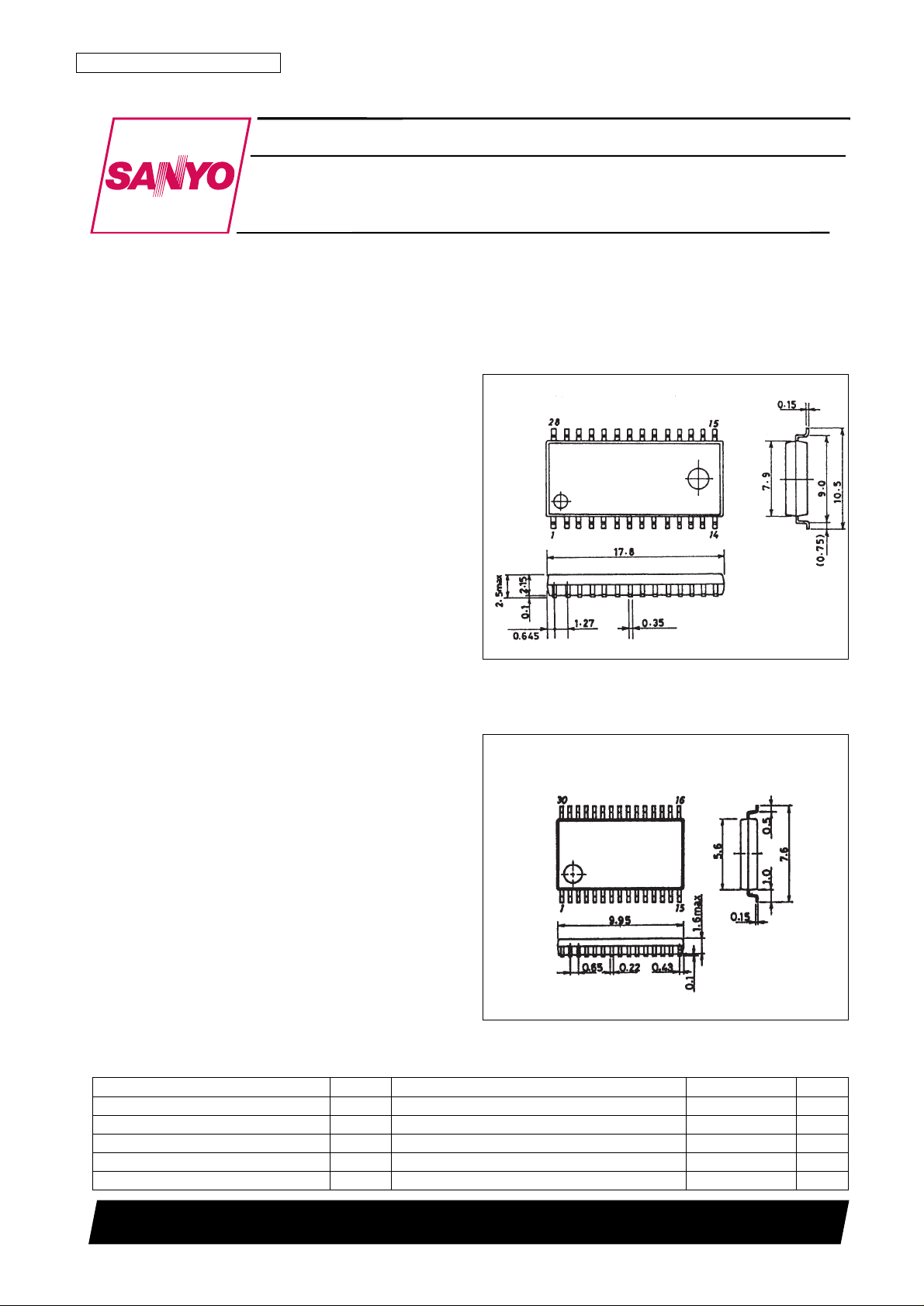
Package Dimensions
unit: mm
3091A-MFP28
unit: mm
3191-SSOP30
CMOS LSI
53096HA (OT)/62095HA (OT) No. 5128-1/8
Preliminaly
SANYO: MFP28
[LC78856M]
SANYO: SSOP30
[LC78856V]
SANYO Electric Co.,Ltd. Semiconductor Bussiness Headquarters
TOKYO OFFICE Tokyo Bldg., 1-10, 1 Chome, Ueno, Taito-ku, TOKYO, 110 JAPAN
Built-in Digital Filter D/A Converters
for Digital Audio
LC78856M, 78856V
Ordering number : EN*5128A
Parameter Symbol Conditions Ratings Unit
Maximum supply voltage V
DD
max –0.3 to +7.0 V
Maximum input voltage V
IN
max –0.3 to VDD+ 0.3 V
Maximum output voltage V
OUT
max –0.3 to VDD+ 0.3 V
Operating temperature Topr –30 to +75 °C
Storage temperature Tstg –40 to +125 °C
Specifications
Absolute Maximum Ratings at Ta = 25°C

No. 5128-2/8
LC78856M, 78856V
Parameter Symbol Conditions
Ratings
Unit
min typ max
Supply voltage V
DD
3.0 5.5 V
Input voltage V
IN
0 V
DD
V
Allowable Operating Ranges at Ta = –30 to +75°C
Parameter Symbol Conditions
Ratings
Unit
min typ max
Input high-level voltage (1) V
IH
1 The XIN pin 0.7 V
DD
V
Input low-level voltage (1) V
IL
1 The XIN pin 0.3 V
DD
V
Input high-level voltage (2) V
IH
2 Pins other than the XIN pin 2.2 V
Input low-level voltage (2) V
IL
2 Pins other than the XIN pin 0.8 V
Output high-level voltage V
OHIOH
= –1 µA VDD– 0.1 V
Output low-level voltage V
OLIOL
= 1 µA 0.1 V
Power dissipation Pd V
DD
= 5.0 V 140 200 mW
DC Characteristics at Ta = –30 to +75°C, VDD= 4.5 to 5.5 V, VSS= 0 V
Parameter Symbol Conditions
Ratings
Unit
min typ max
Oscillator frequency f
X
16.9 18.5 MHz
BCLK frequency f
BCX
2.4 MHz
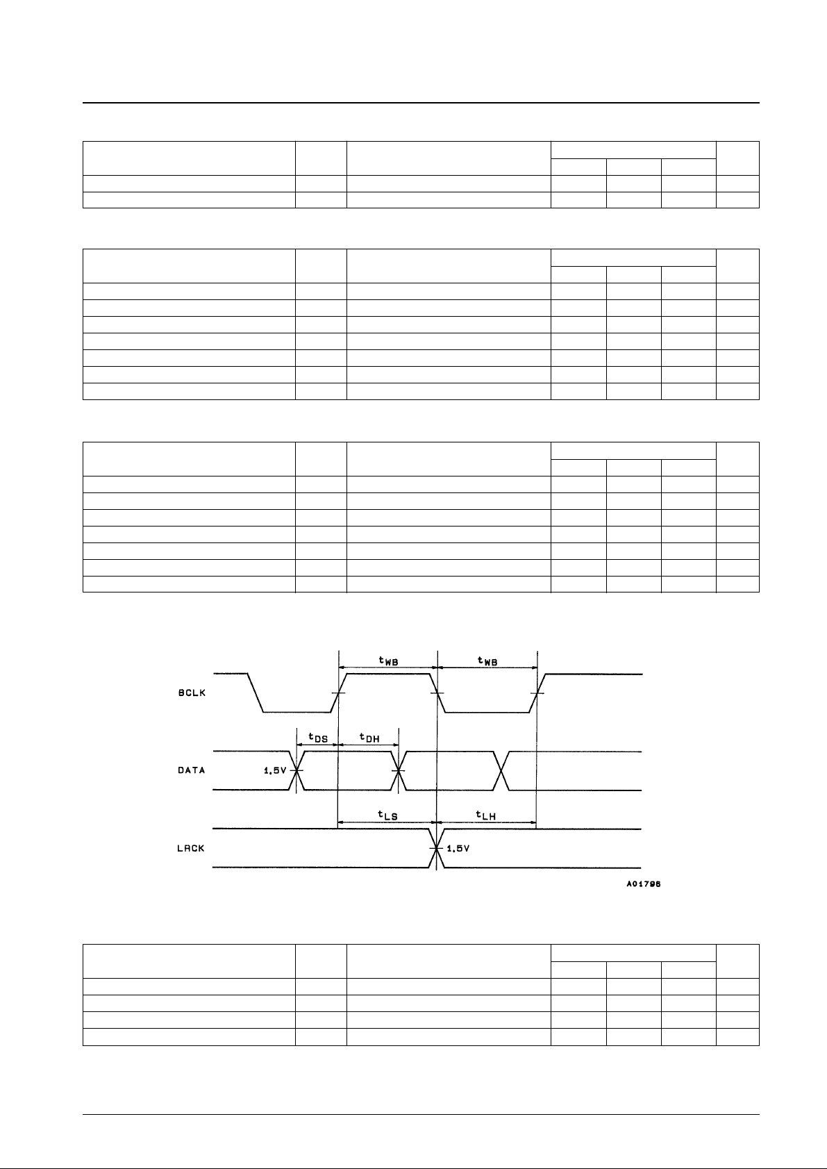
BCLK pulse width t
WB
100 ns
Data setup time t
DS
20 ns
Data hold time t
DH
20 ns
LRCK setup time t
LS
50 ns
LRCK hold time t
LH
50 ns
DC Characteristics at Ta = –30 to +75°C, VDD= 4.5 to 5.5 V, VSS= 0 V
Timing Chart
Parameter Symbol Conditions
Ratings
Unit
min typ max
Total harmonic distortion THD + N f = 1 kHz, 0 dB 0.005 %
Signal-to-noise ratio S/N JIS-A 100 dB
Crosstalk CT f = 1 kHz, 0 dB 98 dB
Dynamic range DR JIS-A 94 dB
Analog Characteristics at Ta = 25°C, VDD= 5.0 V

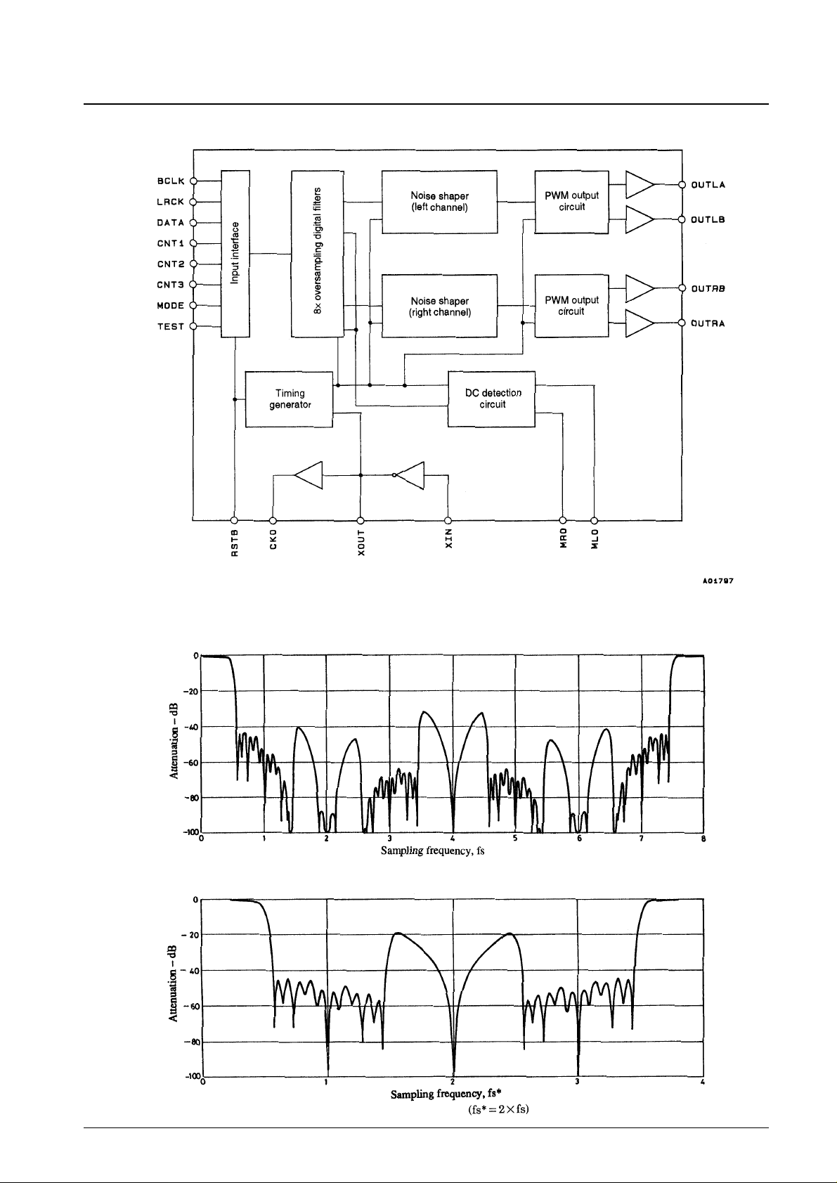
Block Diagram
No. 5128-3/8
LC78856M, 78856V
Filter Characteristics
Standard Speed (de-emphasis off)
Double Speed (de-emphasis off)
 Loading...