

Overview
The LC78856M and LC78856V are ∑∆-type digital-audio
D/A converter circuits with built-in digital filters.
Features
•8× oversampling digital filter
• Digital de-emphasis (supports fs = 44.1 kHz)
• Soft muting
• Double speed support
• Support for a 384fs system clock
• PWM outputs
• 5 V single-voltage power supply
• Si-gate CMOS process
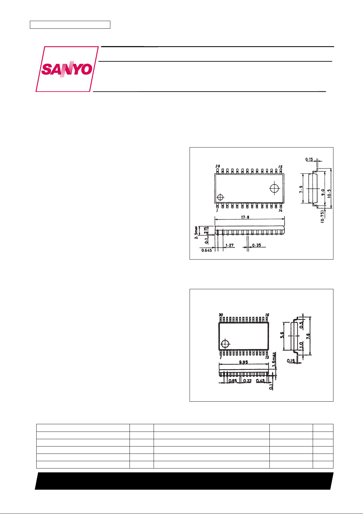
Package Dimensions
unit: mm
3091A-MFP28
unit: mm
3191-SSOP30
CMOS LSI
53096HA (OT)/62095HA (OT) No. 5128-1/8
Preliminaly
SANYO: MFP28
[LC78856M]
SANYO: SSOP30
[LC78856V]
SANYO Electric Co.,Ltd. Semiconductor Bussiness Headquarters
TOKYO OFFICE Tokyo Bldg., 1-10, 1 Chome, Ueno, Taito-ku, TOKYO, 110 JAPAN
Built-in Digital Filter D/A Converters
for Digital Audio
LC78856M, 78856V
Ordering number : EN*5128A
Parameter Symbol Conditions Ratings Unit
Maximum supply voltage V
DD
max –0.3 to +7.0 V
Maximum input voltage V
IN
max –0.3 to VDD+ 0.3 V
Maximum output voltage V
OUT
max –0.3 to VDD+ 0.3 V
Operating temperature Topr –30 to +75 °C
Storage temperature Tstg –40 to +125 °C
Specifications
Absolute Maximum Ratings at Ta = 25°C
No. 5128-2/8
LC78856M, 78856V
Parameter Symbol Conditions
Ratings
Unit
min typ max
Supply voltage V
DD
3.0 5.5 V
Input voltage V
IN
0 V
DD
V
Allowable Operating Ranges at Ta = –30 to +75°C
Parameter Symbol Conditions
Ratings
Unit
min typ max
Input high-level voltage (1) V
IH
1 The XIN pin 0.7 V
DD
V
Input low-level voltage (1) V
IL
1 The XIN pin 0.3 V
DD
V
Input high-level voltage (2) V
IH
2 Pins other than the XIN pin 2.2 V
Input low-level voltage (2) V
IL
2 Pins other than the XIN pin 0.8 V
Output high-level voltage V
OHIOH
= –1 µA VDD– 0.1 V
Output low-level voltage V
OLIOL
= 1 µA 0.1 V
Power dissipation Pd V
DD
= 5.0 V 140 200 mW
DC Characteristics at Ta = –30 to +75°C, VDD= 4.5 to 5.5 V, VSS= 0 V
Parameter Symbol Conditions
Ratings
Unit
min typ max
Oscillator frequency f
X
16.9 18.5 MHz
BCLK frequency f
BCX
2.4 MHz
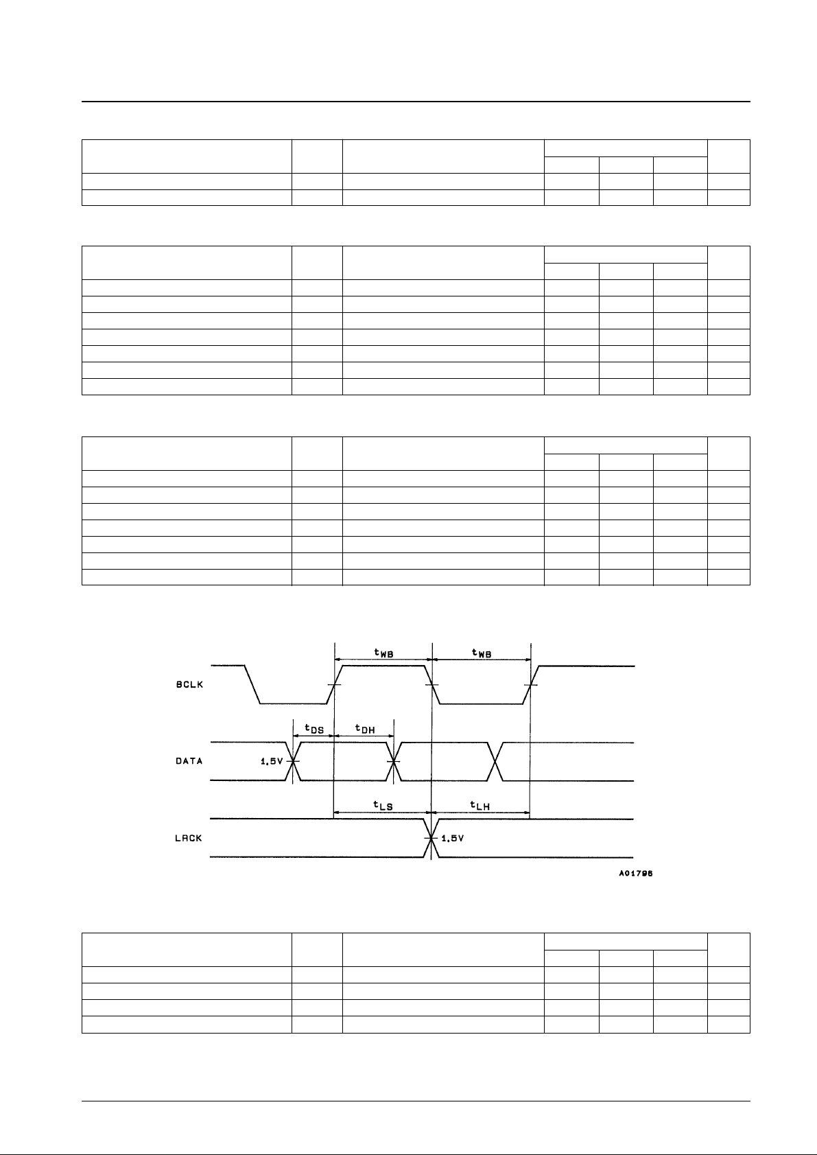
BCLK pulse width t
WB
100 ns
Data setup time t
DS
20 ns
Data hold time t
DH
20 ns
LRCK setup time t
LS
50 ns
LRCK hold time t
LH
50 ns
DC Characteristics at Ta = –30 to +75°C, VDD= 4.5 to 5.5 V, VSS= 0 V
Timing Chart
Parameter Symbol Conditions
Ratings
Unit
min typ max
Total harmonic distortion THD + N f = 1 kHz, 0 dB 0.005 %
Signal-to-noise ratio S/N JIS-A 100 dB
Crosstalk CT f = 1 kHz, 0 dB 98 dB
Dynamic range DR JIS-A 94 dB
Analog Characteristics at Ta = 25°C, VDD= 5.0 V
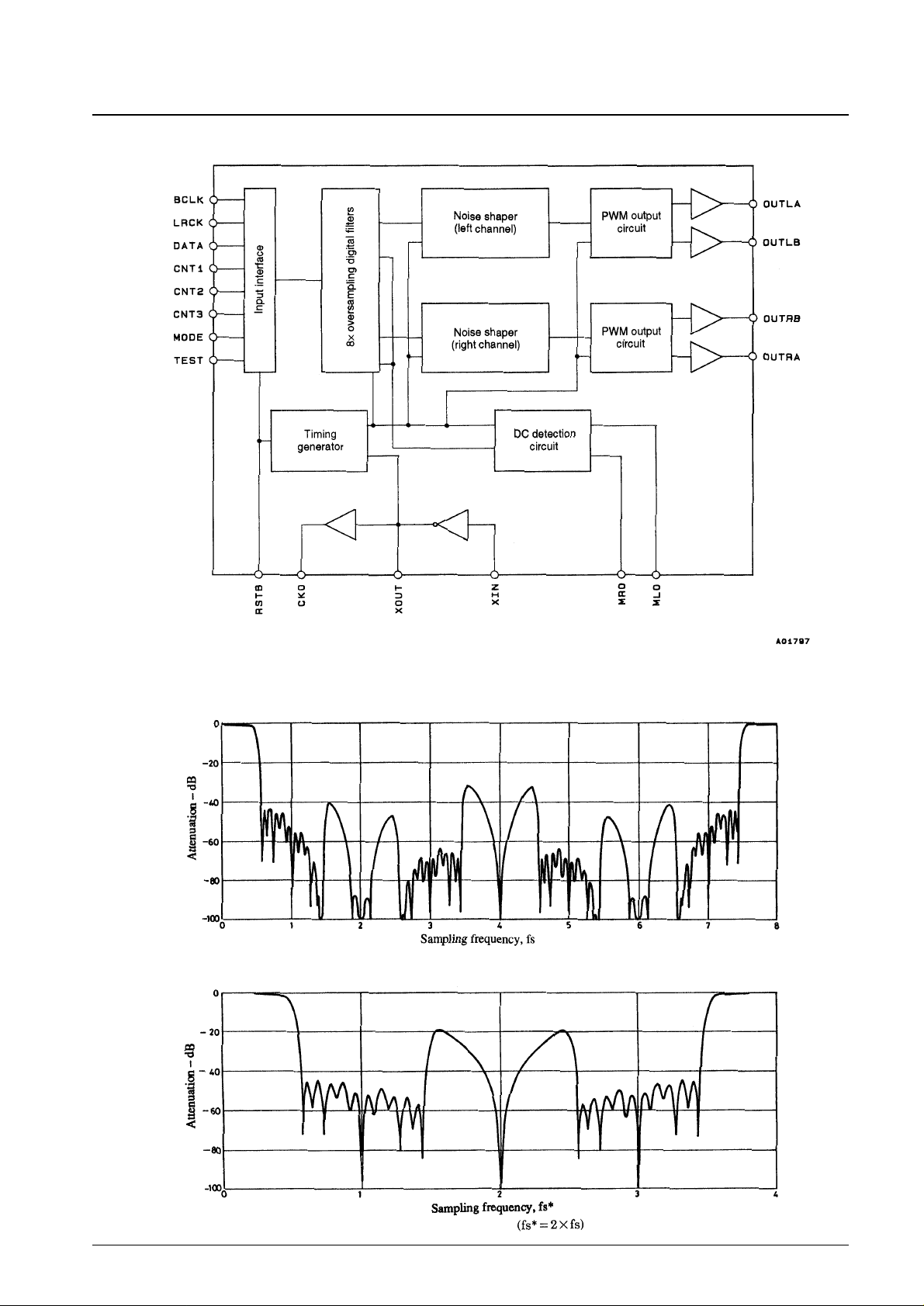
Block Diagram
No. 5128-3/8
LC78856M, 78856V
Filter Characteristics
Standard Speed (de-emphasis off)
Double Speed (de-emphasis off)

Pin Assignments
No. 5128-4/8
LC78856M, 78856V

No. 5128-5/8
LC78856M, 78856V
Pin Functions
SSOP MFP Symbol Function
1 1 RSTB Reset input (A low-level input resets the LSI internal circuits.)
2 2 CNT1 Emphasis on/off switching input
3 3 CNT2 Standard speed/double speed switching input
4 4 CNT3 Soft mute input
5 5 BCLK Bit clock input
6 6 LRCK LR clock input
7 7 DATA Digital audio data input
10 8 MODE Input format setting
11 9 CKO Clock output
12 10 XV
DD
Oscillator amplifier power supply
13 11 XIN Oscillator amplifier input
14 12 XOUT Oscillator amplifier output
15 13 XGND Oscillator amplifier ground
16 14 DGND Digital system ground
17 15 MRO Right channel mute signal output
18 16 TEST Test pin (Must be tied low in normal operation.)
19 17 AV
DD
4 Analog system power supply
20 18 OUTRA Right channel output A
21 19 AGND2 Analog system ground
22 20 OUTRB Right channel output B
23 21 AV
DD
3 Analog system power supply
24 22 AV
DD
2 Analog system power supply
25 23 OUTLB Left channel output B
26 24 AGND1 Analog system ground
27 25 OUTLA Left channel output A
28 26 AV
DD
1 Analog system power supply
29 27 MLO Left channel mute signal output
30 28 DV
DD
Digital system power supply
Operating Description
The LC78856M and LC78856V internal circuits can be roughly divided into the digital filter block and the 1-bit D/A
converter block.
[Digital Filter Block]
1. Standard Speed
The LC78856M and LC78856V implements 8× oversampling using three FIR filters: a 43rd-order filter, an 11thorder filter, and a 3rd-order filter. A 1st-order IIR filter is used for de-emphasis.
2. Double Speed
Double-speed playback is used, for example, for dubbing CDs to audio tape at double speed. Here, the same
frequency is used for XIN, but BCLK, LRCK and DATA are input at twice the rates used in standard-speed
playback. After de-emphasis is applied with a 1st-order IIR filter, the signal is 4× oversampled using a 43rd-order
FIR filter and a 3rd-order FIR filter.

3. One-Bit D/A Converter Block
The 1-bit D/A converter accepts 8fs data input and outputs a 384fs 1-bit data stream.
LC78856M/V Inputs
1. Input Data Format
• Format 1 (MODE = high)
• Format 2 (MODE = low)
2. Control Signals (CNT1 to CNT3)
3. Initialization
The LC78856M and LC78856V requires initialization when power is first applied and when settings are changed.
The LC78856M and LC78856V is initialized by setting the RSTB pin low. The length of the low-level period must
extend 1 µs beyond the point where the XIN input is applied. When RSTB is low, all digital filter and noise shaper
internal data is set to 0, and the D/A converter outputs an analog 0.
No. 5128-6/8
LC78856M, 78856V
Symbol Function L H
CNT1 Emphasis switching Off On
CNT2 Standard speed/double speed Standard speed Double speed
CNT3 Soft mute Off On

LC78856M/V Outputs
1. CKO
CKO outputs a clock signal with the same frequency as the signal input to the XIN pin.
2. MLO, MRO
These pins output a high level when either the attenuator coefficient has become 0, or when the corresponding
channel data has been 0 for 213or more cycles.
3. OUTLA, OUTLB, OUTRA, OUTRB
These four pins produce outputs in synchronization with the XIN clock. High-precision analog signals can be
acquired by differentially amplifying the output signals and passing that result through an LPF. The figure below
shows a sample circuit structure.
Sample Output Circuit Structure
No. 5128-7/8
LC78856M, 78856V

No. 5128-8/8
LC78856M, 78856V
Sample Application Circuit
This catalog provides information as of December, 1997. Specifications and information herein are subject to
change without notice.
■ No products described or contained herein are intended for use in surgical implants, life-support systems, aerospace
equipment, nuclear power control systems, vehicles, disaster/crime-prevention equipment and the like, the failure of
which may directly or indirectly cause injury, death or property loss.
■ Anyone purchasing any products described or contained herein for an above-mentioned use shall:
➀ Accept full responsibility and indemnify and defend SANYO ELECTRIC CO., LTD., its affiliates, subsidiaries and
distributors and all their officers and employees, jointly and severally, against any and all claims and litigation and all
damages, cost and expenses associated with such use:
➁ Not impose any responsibility for any fault or negligence which may be cited in any such claim or litigation on
SANYO ELECTRIC CO., LTD., its affiliates, subsidiaries and distributors or any of their officers and employees
jointly or severally.
■ Information (including circuit diagrams and circuit parameters) herein is for example only; it is not guaranteed for
volume production. SANYO believes information herein is accurate and reliable, but no guarantees are made or implied
regarding its use or any infringements of intellectual property rights or other rights of third parties.
 Loading...