

Page 1

Overview
The LC78622E is a CMOS LSI that implements the signal
processing and servo control required by compact disc
players. At the same time as providing an EFM PLL
circuit, a 1-bit D/A converter, and an analog low-pass
filter the LC78622E realizes an optimal cost-performance
tradeoff for low-end players by strictly limiting
functionality to basic signal-processing and servo system
functionality. The LC78622E signal-processing system
provides demodulation of the EFM signal from the pickup,
de-interleaving, error detection and correction, and digital
filters that can prove useful in reducing the cost of end
products. The LC78622E servo control system processes
servo commands sent from the control microprocessor.
Functions
• Input signal processing: The LC78622E takes an HF
signal as input, digitizes (slices) that signal at a precise
level, converts that signal to an EFM signal, and
generates a PLL clock with an average frequency of
4.3218 MHz by comparing the phases of that signal and
an internal VCO.
• Precise reference clock and necessary internal timing
generation using an external 16.9344 MHz crystal
oscillator
• Disk motor speed control using a frame phase difference
signal generated from the playback clock and the
reference clock
• Frame synchronization signal detection, protection and
interpolation to assure stable data readout
• EFM signal demodulation and conversion to 8-bit
symbol data
• Subcode data separation from the EFM demodulated
signal and output of that data to an external
microprocessor
• Subcode Q signal output to a microprocessor over the
serial I/O interface after performing a CRC error check
(LSB first)
• Demodulated EFM signal buffering in internal RAM to
handle up to ±4 frames of disk rotational jitter
• Demodulated EFM signal reordering in the prescribed
order for data unscrambling and de-interleaving
• Error detection, correction, and flag processing (error
correction scheme: dual C1 plus dual C2 correction)
• The LC78622E sets the C2 flags based on the C1 flags
and a C2 check, and then performs signal interpolation
or muting depending on the C2 flags. The interpolation
circuit uses a dual-interpolation scheme. The previous
value is held if the C2 flags indicate errors two or more
times consecutively.
• Support for command input from a control
microprocessor: commands include track jump, focus
start, disk motor start/stop, muting on/off and track
count (8 bit serial input)
• Built-in digital output circuits.
• Arbitrary track counting to support high-speed data
access
• D/A converter outputs with data continuity improved by
4× oversampling digital filters.
• Built-in third-order ∑∆ D/A converters (An analog lowpass filter is built in.)
• Built-in digital attenuator (8 bits – alpha, 239 steps)
• Built-in digital de-emphasis
• Zero cross muting
• Supports the implementation of a double-speed dubbing
function.
• Support for bilingual applications.
• General-purpose I/O ports: 5 pins
Features
• 5 V single-voltage power supply
• Supports low-voltage operation (3.0 V, minimum)
Package Dimensions
unit: mm
3159-QFP64E
CMOS LSI
93096HA (OT) No. 5467-1/29
SANYO: QFP64E
[LC78622E]
SANYO Electric Co.,Ltd. Semiconductor Bussiness Headquarters
TOKYO OFFICE Tokyo Bldg., 1-10, 1 Chome, Ueno, Taito-ku, TOKYO, 110 JAPAN
Compact Disc Player DSP
LC78622E
Ordering number : EN5467
Page 2
No. 5480-2/29
LC78622E
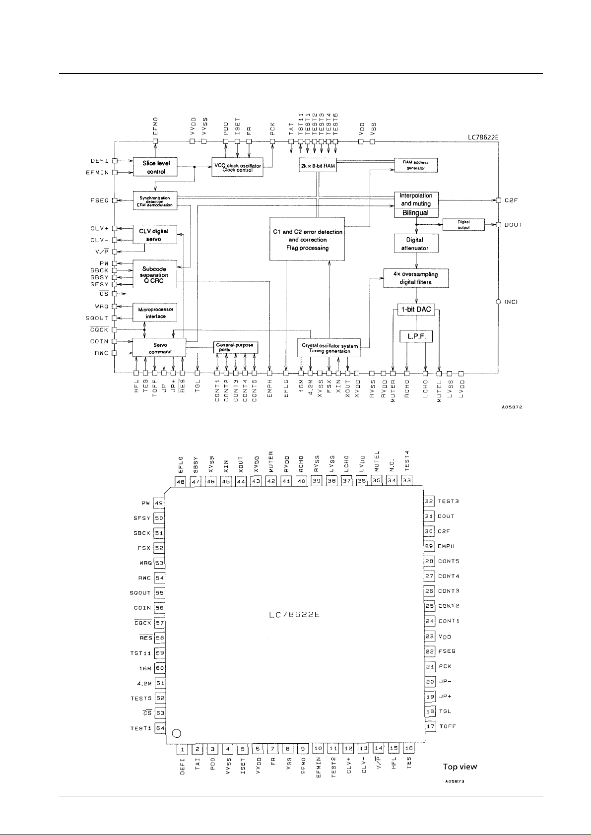
Equivalent Circuit Block Diagram
Pin Assignment
Page 3

No. 5480-3/29
LC78622E
Specifications
Absolute Maximum Ratings at Ta = 25°C, VSS= 0 V
Allowable Operating Ranges at Ta = 25°C, VSS= 0 V
Parameter Symbol Conditions Ratings Unit
Maximum supply voltage V
DD
max VSS– 0.3 to VSS+ 7.0 V
Input voltage V
IN
VSS– 0.3 to VDD+ 0.3 V
Output voltage V
OUT
VSS– 0.3 to VDD+ 0.3 V
Allowable power dissipation Pd max 300 mW
Operating temperature Topr –20 to +75 °C
Storage temperature Tstg –40 to +125 °C
Parameter Symbol Conditions min typ max Unit
V
DD
(1)
V
DD
, XVDD, LVDD, RVDD, VVDD:
3.0 5.5 V
During normal-speed playback
Supply voltage
V
DD
(2)
V
DD
, XVDD, LVDD, RVDD, VVDD:
3.6 5.5 V
During double-speed playback
V
IH
(1)
DEFI, COIN, RES, HFL, TES, SBCK, RWC, CQCK,
Input high level voltage
TAI, TEST1 to TEST5, CS, CONT1 to CONT5
0.7 V
DD
V
DD
V
V
IH
(2) EFMIN 0.6 V
DD
V
DD
V
V
IL
(1)
DEFI, COIN, RES, HFL, TES, SBCK, RWC, CQCK,
Input low level voltage
TAI, TEST1 to TEST5, CS, CONT1 to CONT5
0 0.3 V
DD
V
VIL(2) EFMIN 0 0.4 V
DD
V
Data setup time t
SU
COIN, RWC: Figure 1 400 ns
Data hold time t
HD
COIN, RWC: Figure 1 400 ns
High level clock pulse width t
WH
SBCK, CQCK: Figures 1, 2 and 3 400 ns
Low level clock pulse width t
WL
SBCK, CQCK: Figures 1, 2 and 3 400 ns
Data read access time t
RAC
SQOUT, PW: Figures 2 and 3 0 400 ns
Command transfer time t
RWC
RWC: Figure 1 1000 ns
Subcode Q read enable time t
SQE
WRQ: Figure 2, with no RWC signal 11.2 ms
Subcode read cycle time t
SC
SFSY: Figure 3 136 µs
Subcode read enable time t
SE
SFSY: Figure 3 400 ns
Port input data setup time t
CSU
CONT1 to CONT5, RWC: Figure 4 400 ns
Port input data hold time t
CHD
CONT1 to CONT5, RWC: Figure 4 400 ns
Port input clock setup time t
RCQ
RWC, CQCK: Figure 4 100 ns
Port output data delay time t
CDD
CONT1 to CONT5, RWC: Figure 5 1200 ns
Input level
V
IN
(1) EFMIN: Slice level control 1.0 Vp-p
V
IN
(2) XIN: Capacitor-coupled input 1.0 Vp-p
Operating frequency range fop EFMIN 10 MHz
Crystal oscillator frequency f
X
XIN, X
OUT
16.9344 MHz
Page 4

No. 5480-4/29
LC78622E
Electrical Characteristics at Ta = 25°C, VDD= 5 V, VSS= 0 V
One-Bit D/A Converter Analog Characteristics
at Ta = 25°C, VDD= LVDD= RVDD= 5 V, VSS= LVSS= RVSS= 0 V
Note: Measured with the normal-speed playback mode in the Sanyo one-bit D/A converter block reference digital attenuator circuit set to EE (hexadecimal).
Parameter Symbol Conditions min typ max Unit
Current drain I
DD
VDD, XVDD, LVDD, RVDD, VV
DD
25 35 mA
DEFI, EFMIN, COIN, RES, HFL, TES, SBCK,
Input high level current
I
IH
(1)
RWC, CQCK: TEST1: V
IN
= V
DD
5 µA
I
IH
(2) TAI, TEST2 to TEST5, CS: VIN= VDD= 5.5 V 25 75 µA
DEFI, EFMIN, COIN, RES, HFL, TES, SBCK,
Input low level current I
IL
RWC, CQCK: TAI, TEST1 to TEST5, CS: VIN= 0 V
–5 µA
EFMO, CLV
+
, CLV–, V/P, PCK, FSEQ, TOFF,
V
OH
(1)
TGL, JP
+
, JP–, EMPH, EFLG, FSX: IOH= –1 mA
4 V
MUTEL, MUTER, C2F, SBSY, PW, SFSY, WRQ,
Output high level voltage
V
OH
(2) SQOUT, TST11, 16M, 4.2M, CONT1 to CONT5: 4 V
I
OH
= –0.5 mA
V
OH
(3) DOUT: IOH= –12 mA 4.5 V
EFMO, CLV
+
, CLV–, V/P, PCK, FSEQ,
V
OL
(1) TOFF, TGL, JP+, JP–, EMPH, EFLG, FSX: 1 V
I
OH
= 1 mA
Output low level voltage
MUTEL, MUTER,
V
OL
(2)
C2F, SBSY, PW, SFSY, WRQ, SQOUT,
0.4 V
TST11, 16M, 4.2M, CONT1 to CONT5:
I
OH
= 2 mA
V
OL
(3) DOUT: IOH= 12 mA 0.5 V
I
OFF
(1)
PDO, CLV
+
, CLV–, JP+, JP–, CONT1 to CONT5:
5 µA
V
OUT
= V
DD
Output off leakage current
I
OFF
(2)
PDO, CLV
+
, CLV–, JP+, JP–, CONT1 to CONT5:
–5 µA
V
OUT
= 0 V
Charge pump output current
I
PDOH
PDO: R
ISET
= 68 kΩ 64 80 96 µA
I
PDOL
PDO: R
ISET
= 68 kΩ –96 –80 –64 µA
Parameter Symbol Conditions min typ max Unit
Total harmonic distortion THD + N
LCHO, RCHO; 1 kHz: 0 dB data input,
0.011 0.013 %
using the 20 kHz low-pass filter (AD725D built in)
LCHO, RCHO; 1 kHz: –60 dB data input,
Dynamic range DR using the 20 kHz low-pass filter and the A filter 91 92 dB
(AD725D built in)
LCHO, RCHO; 1 kHz: 0 dB data input,
Signal-to-noise ratio S/N using the 20 kHz low-pass filter and the A filter 93 95 dB
(AD725D built in)
Crosstalk CT
LCHO, RCHO; 1 kHz: 0 dB data input,
82 84 dB
using the 20 kHz low-pass filter (AD725D built in)
Page 5

No. 5480-5/29
LC78622E
Figure 1 Command Input
Figure 2 Subcode Q Output
Figure 3 Subcode Output
Page 6

No. 5480-6/29
LC78622E
Figure 4 General-Purpose Port Input Timing
Figure 5 General-Purpose Port Output Timing
Page 7

No. 5480-7/29
LC78622E
Pin Functions
Pin No. Symbol I/O Function
1 DEFI I Defect detection signal (DEF) input. (Must be connected to 0 V when unused.)
2 TAI I Test input. A pull-down resistor is built in. Must be connected to 0 V.
3 PDO O External VCO control phase comparator output
4 VV
SS
–
PLL pins
Internal VCO ground. Must be connected to 0 V.
5 ISET AI PDO output current adjustment resistor connection
6 VV
DD
– Internal VCO power supply
7 FR AI VCO frequency range adjustment
8 V
SS
– Digital system ground. Must be connected to 0 V.
9 EFMO O
Slice level control
EFM signal output
10 EFMIN I EFM signal input
11 TEST2 I Test input. A pull-down resistor is built in. Must be connected to 0 V.
12 CLV
+
O
Disc motor control output.
13 CLV
–
O Three-value output is also possible when specified by microprocessor command.
14 V/P O
Rough servo/phase control automatic switching monitor output. Outputs a high level during rough servo and a low level
during phase control.
15 HFL I Track detection signal input. This is a Schmitt input.
16 TES I Tracking error signal input. This is a Schmitt input.
17 TOFF O Tracking off output
18 TGL O Tracking gain switching output. Increase the gain when low.
19 JP
+
O
Track jump output.
20 JP
–
O Three-value output is also possible when specified by microprocessor command.
21 PCK O EFM data playback clock monitor. Outputs 4.3218 MHz when the phase is locked.
22 FSEQ O
Synchronization signal detection output. Outputs a high level when the synchronization signal detected from the EFM
signal and the internally generated synchronization signal agree.
23 V
DD
– Digital system power supply.
24 CONT1 I/O General-purpose I/O pin 1
25 CONT2 I/O General-purpose I/O pin 2
Controlled by serial data commands from the microprocessor. Any of these that are unused
26 CONT3 I/O General-purpose I/O pin 3 must be either set up as input ports and connected to 0 V, or set up as output ports and
27 CONT4 I/O General-purpose I/O pin 4
left open.
28 CONT5 I/O General-purpose I/O pin 5
29 EMPH O De-emphasis monitor pin. A high level indicates playback of a de-emphasis disk.
30 C2F O C2 flag output
31 DOUT O Digital output. (EIAJ format)
32 TEST3 I Test input. A pull-down resistor is built in. Must be connected to 0 V.
33 TEST4 I Test input. A pull-down resistor is built in. Must be connected to 0 V.
34 N.C. – Unused. Must be left open.
35 MUTEL O Left channel mute output
36 LV
DD
–
Left channel
Left channel power supply
37 LCHO O one-bit D/A converter Left channel output
38 LV
SS
– Left channel ground. Must be connected to 0 V.
39 RV
SS
– Right channel ground. Must be connected to 0 V.
40 RCHO O
Right channel
Right channel output
41 RV
DD
– one-bit D/A converter Right channel power supply
42 MUTER O Right channel mute output
43 XV
DD
– Crystal oscillator power supply.
44 X
OUT
O
Connections for a 16.9344 crystal oscillator element
45 X
IN
I
46 XV
SS
– Crystal oscillator ground. Must be connected to 0 V.
47 SBSY O Subcode block synchronization signal output
48 EFLG O C1, C2, single and double error correction monitor pin
49 PW O Subcode P, Q, R, S, T, U, V and W output
50 SFSY O Subcode frame synchronization signal output. This signal falls when the subcodes are in the standby state.
Page 8

No. 5480-8/29
LC78622E
Continued from preceding page.
Note: The same potential must be supplied to all power supply pins, i.e., VDD, VVDD, LVDD, RVDD, and XVDD.
Pin Applications
1. HF Signal Input Circuit; Pin 10: EFMIN, pin 9: EFMO, pin 1: DEFI, pin 12: CLV
+
An EFM signal (NRZ) sliced at an optimal level can be acquired
by inputting the HF signal to EFMIN.
The LC78622E handles defects as follows. When a high level is
input to the DEFI pin (pin 1), EFMO (pin 9) pins (the slice level
control outputs) go to the high-impedance state, and the slice
level is held. However, note that this function is only valid in
CLV phase control mode, that is, when the V/P pin (pin 14) is
low. This function can be used in combination with the
LA9230M, LA9231M and LA9240M DEF pins.
Note: If the EFMIN and CLV+signal lines are too close to each
other, unwanted radiation can result in error rate
degradation. We recommend laying a ground or V
DD
shield line between these two lines.
2. PLL Clock Generation Circuit; Pin 3: PDO, pin 5: ISET, pin 7: FR, pin 21: PCK
Since the LC78622E includes a VCO circuit, a PLL circuit can
be formed by connecting an external RC circuit. ISET is the
charge pump reference current, PDO is the VCO circuit loop
filter, and FR is a resistor that determines the VCO frequency
range.
(Reference values)
R1 = 68 kΩ, C1 = 0.1 µF
R2 = 680 Ω, C2 = 0.1 µF
R3 = 1.2 kΩ
The VCO× 2 command is an auxiliary command for characteristics guarantee in low-voltage operations. This
command supports the low-voltage operations at VDD= 3.0 to 3.6 V.
Pin No. Symbol I/O Function
51 SBCK I Subcode readout clock input. This is a Schmitt input. (Must be connected to 0 V when unused.)
52 FSX O Output for the 7.35 kHz synchronization signal divided from the crystal oscillator
53 WRQ O Subcode Q output standby output
54 RWC I Read/write control input. This is a Schmitt input.
55 SQOUT O Subcode Q output
56 COIN I Command input from the control microprocessor
57 CQCK I Input for both the command input clock and the subcode readout clock. This is a Schmitt input.
58 RES I Chip reset input. This pin must be set low briefly after power is first applied.
59 TST11 O Test output. Leave open. (Normally outputs a low level.)
60 16M O 16.9344 MHz output.
61 4.2M O 4.2336 MHz output
62 TEST5 I Test input. A pull-down resistor is built in. Must be connected to 0 V.
63 CS I Chip select input. A pull-down resistor is built in. Must be connected to 0 V if not controlled.
64 TEST1 I Test input. No pull-down resistor. Must be connected to 0 V.
Page 9

No. 5480-9/29
LC78622E
3. VCO Monitor; Pin 21: PCK
PCK is a monitor pin that outputs an average frequency of 4.3218 MHz, which is divided from the VCO frequency.
4. Synchronization Detection Monitor; Pin 22: FSEQ
Pin 22 goes high when the frame synchronization (a positive polarity synchronization signal) from the EFM signal
read in by PCK and the timing generated by the counter (the interpolation synchronization signal) agree. This pin is
thus a synchronization detection monitor. (It is held high for a single frame.)
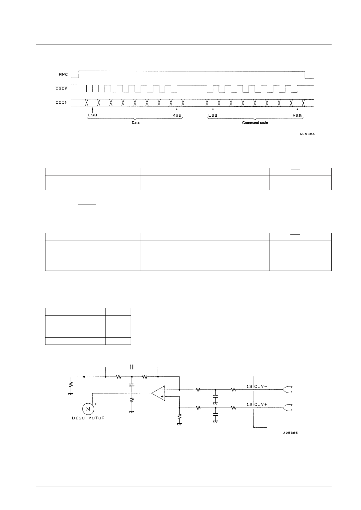
5. Servo Command Function; Pin 54: RWC, pin 56: COIN, pin 57: CQCK
Commands can be executed by setting RWC high and inputting commands to the COIN pin in synchronization with
the CQCKclock. Note that commands are executed on the falling edge of RWC.
Focus start
Track jump
Muting control One-byte commands
Disk motor control
Miscellaneous control
Track check Two-byte command (RWC set twice)
Digital attenuator
General-purpose I/O, E/D
Two-byte commands (RWC set once)
• One-byte commands
• Two-byte commands (RWC set twice: For track checking)
Page 10
No. 5480-10/29
LC78622E
• Two-byte commands (RWC set once: Sets up the digital attenuation and the general-purpose I/O ports)
• Command noise rejection
This command reduces the noise on the CQCK clock signal. While this is effective for noise pulses shorter than
500 ns, the CQCK timings tWL, tWH, and tSU, must be set for at least 1 µs.
6. CLV Servo Circuit; Pin 12: CLV+, pin 13: CLV–, pin 14: V/P
The CLV+pin provides the signal that accelerates the disk in the forward direction and the CLV–pin provides the
signal that decelerates the disk. Commands from the control microprocessor select one of four modes; accelerate,
decelerate, CLV and stop. The table below lists the CLV+and CLV–outputs in each of these modes.
Note: CLV servo control commands can set the TOFF pin low only in CLV mode. That pin will be at the high level
at all other times. Control of the TOFF pin by microprocessor command is only valid in CLV mode.
MSB LSB Command RES = low
1 1 1 0 1 1 1 1 COMMAND INPUT NOISE REDUCTION MODE
1 1 1 0 1 1 1 0 RESET NOISE EXCLUSION MODE
●●
MSB LSB Command RES = low
0 0 0 0 0 1 0 0 DISC MOTOR START (accelerate)
0 0 0 0 0 1 0 1 DISC MOTOR CLV (CLV)
0 0 0 0 0 1 1 0 DISC MOTOR BRAKE (decelerate)
0 0 0 0 0 1 1 1 DISC MOTOR STOP (stop)
●●
Mode CLV
+
CLV
–
Accelerate High Low
Decelerate Low High
CLV
Pulse output Pulse output
Stop Low Low
Page 11
No. 5480-11/29
LC78622E
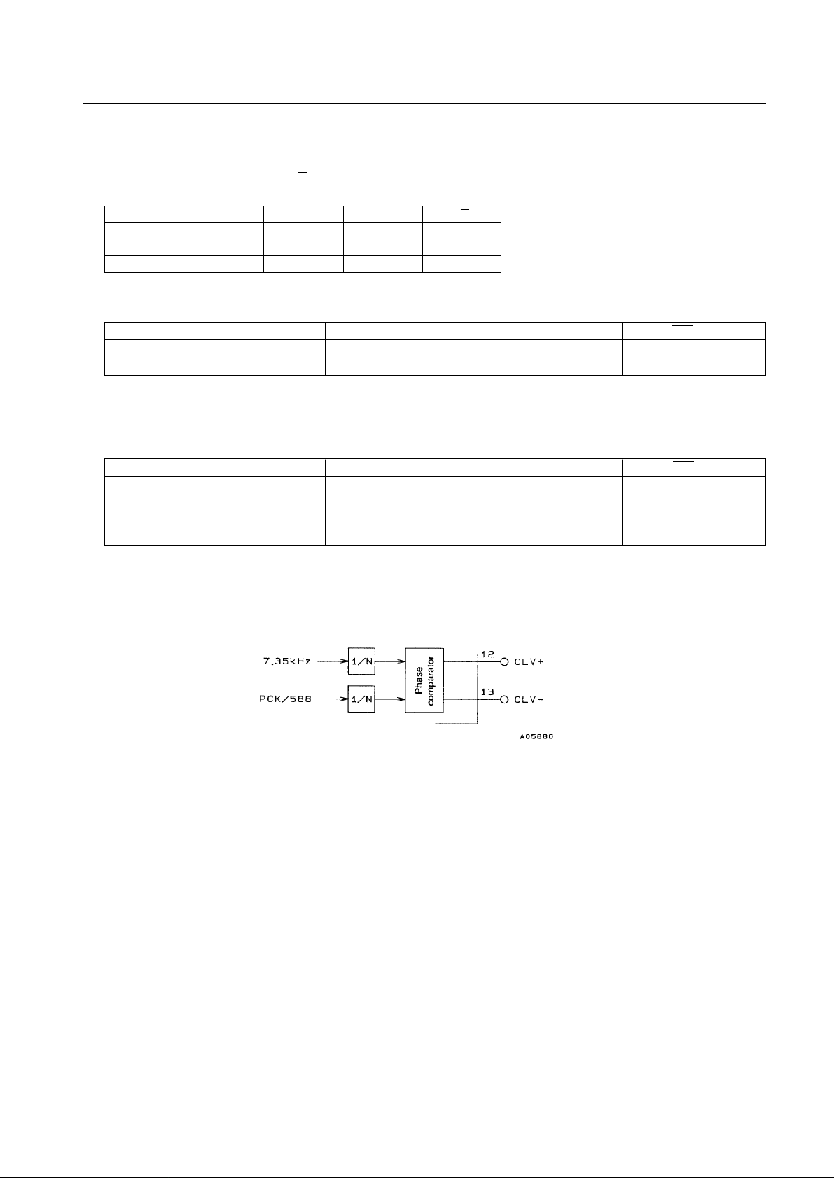
• CLV mode
In CLV mode the LC78622E detects the disk speed from the HF signal and provides proper linear speed using
several different control schemes by switching the DSP internal modes. The PWM reference period corresponds to
a frequency of 7.35 kHz. The V/P pin outputs a high level during rough servo and a low level during phase control.
• Rough servo gain switching
For 8 cm disks, the rough servo mode CLV control gain can be set about 8.5 dB lower than the gain used for 12 cm
disks.
• Phase control gain switching
The phase control gain can be changed by changing the divisor used by the dividers in the stage immediately
preceding the phase comparator.
Internal mode CLV
+
CLV
–
V/P
Rough servo (velocity too low) High Low High
Rough servo (velocity too high) Low High High
Phase control (PCK locked) PWM PWM Low
MSB LSB Command RES= low
1 0 1 1 0 0 0 1 CLV PHASE COMPARATOR DIVISOR: 1/2
1 0 1 1 0 0 1 0 CLV PHASE COMPARATOR DIVISOR: 1/4
1 0 1 1 0 0 1 1 CLV PHASE COMPARATOR DIVISOR: 1/8
1 0 1 1 0 0 0 0 NO CLV PHASE COMPARATOR DIVISOR USED
●●
MSB LSB Command RES = low
1 0 1 0 1 0 0 0 DISC 8 SET
1 0 1 0 1 0 0 1 DISC 12 SET
●●
Page 12
No. 5480-12/29
LC78622E
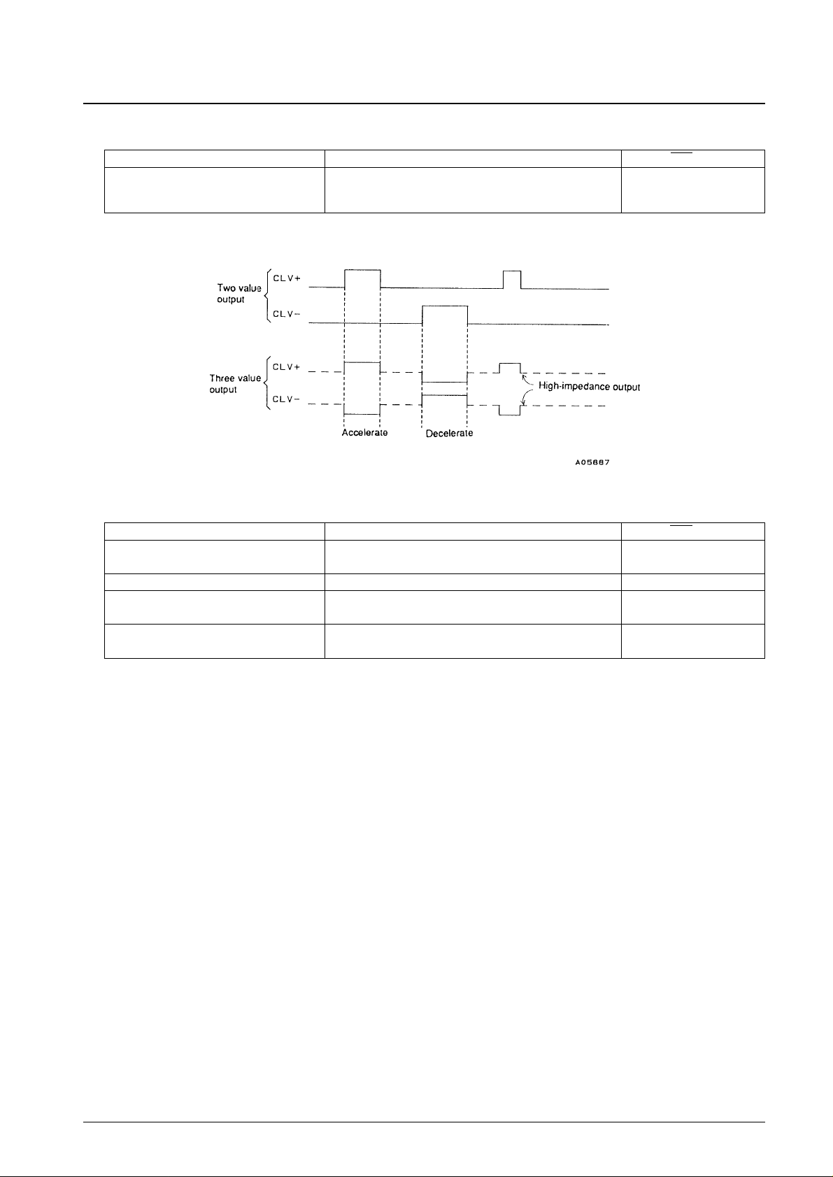
• CLV three-value output
The CLV three-value output command allows the CLV to be controlled by a single pin.
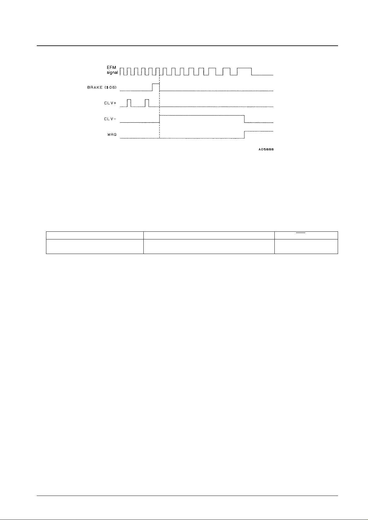
• Internal brake modes
— Issuing the internal brake-on (C5H) command sets the LC78622E to internal brake mode. In this mode, the disk
deceleration state can be monitored from the WRQ pin when a brake command (06H) is executed.
— In this mode the disk deceleration state is determined by counting the EFM signal density in a single frame, and
when the EFM signal count falls under four, the CLV–pin is dropped to low. At the same time the WRQ signal,
which functions as a brake completion monitor, goes high. When the microprocessor detects a high level on the
WRQ signal, it should issue a STOP command to fully stop the disk. In internal brake continuous mode (CBH),
the CLV–pin high-level output braking operation continues even after the WRQ brake completion monitor
goes high.
Note that if errors occur in deceleration state determination due to noise in the EFM signal, the problem may be
rectified by changing the EFM signal count from four to eight with the internal brake control command (A3H).
— In TOFF output disabled mode (CDH), the TOFF pin is held low during internal brake operations. We
recommend using this feature, since it is effective at preventing incorrect detection at the disk mirror surface.
MSB LSB Command RES = low
1 1 0 0 0 1 0 1 INTERNAL BRAKE ON
1 1 0 0 0 1 0 0 INTERNAL BRAKE OFF
●●
1 0 1 0 0 0 1 1 INTERNAL BRAKE CONTROL
1 1 0 0 1 0 1 1 INTERNAL BRAKE CONTINUOUS MODE
1 1 0 0 1 0 1 0 RESET CONTINUOUS MODE
●●
1 1 0 0 1 1 0 1 TON MODE DURING INTERNAL BRAKING
1 1 0 0 1 1 0 0 RESET TON MODE
●●
MSB LSB Command RES = low
1 0 1 1 0 1 0 0 CLV THREE VALUE OUTPUT
1 0 1 1 0 1 0 1
CLV TWO VALUE OUTPUT
●●
(the scheme used by previous products)
Page 13
No. 5480-13/29
LC78622E
Note: 1. If focus is lost during the execution of an internal brake command, the pickup must first be refocussed
and then the internal brake command must be reissued.
2. Since incorrect deceleration state determination is possible depending on the EFM signal playback state
(e.g., disk defects, access in progress), we recommend using these functions in combination with a
microprocessor.
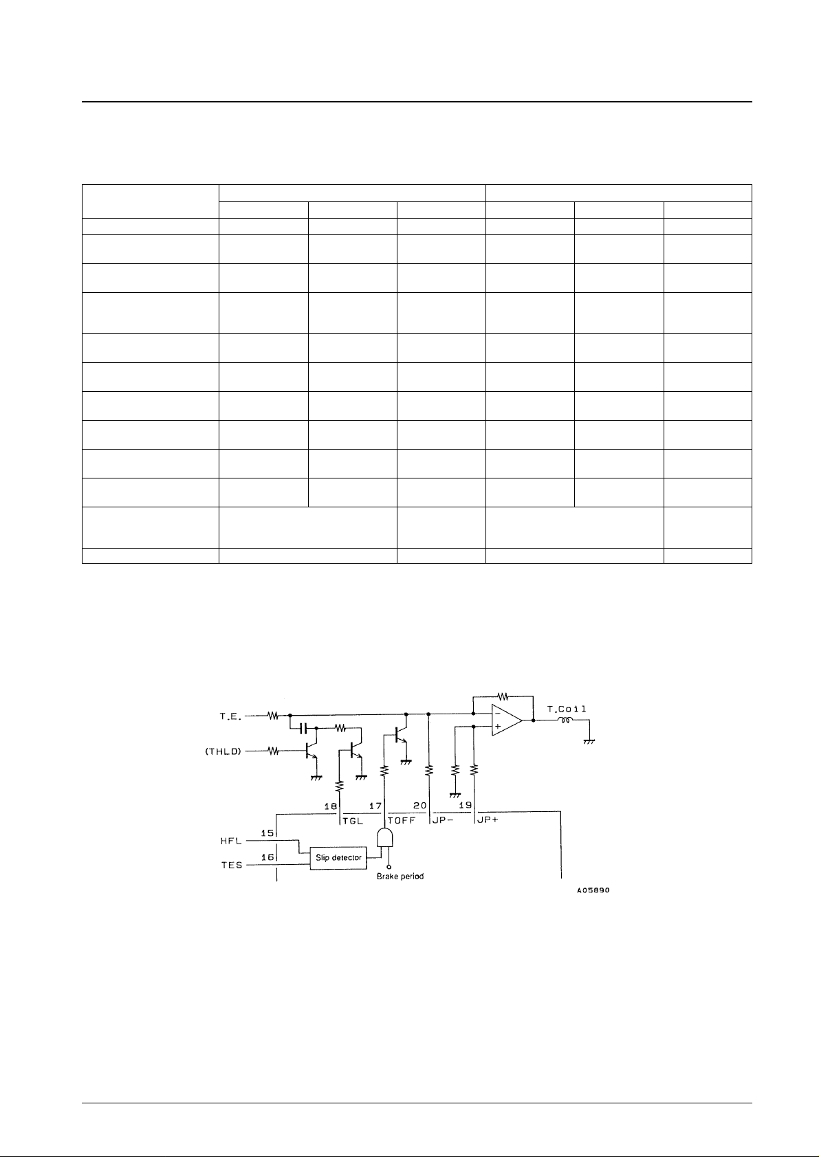
7. Track Jump Circuit; Pin 15: HFL, pin 16: TES, pin 17: TOFF, pin 18: TGL, pin 19: JP+, pin 20: JP
–
• The LC78622E supports the two track count modes listed below.
The earlier track count function uses the TES signal directly as the internal track counter clock.
To reduce counting errors resulting from noise on the rising and falling edges of the TES signal, the new track
count function prevents noise induced errors by using the combination of the TES and HFL signals, and
implements a more reliable track count function. However, dirt and scratches on the disk can result in HFL signal
dropouts that may result in missing track count pulses. Thus care is required when using this function.
MSB LSB Command RES = low
0 0 1 0 0 0 1 0 NEW TRACK COUNT (using the TES/HFL combination)
●●
0 0 1 0 0 0 1 1 STANDARD TRACK COUNT (directly counts the TES signal)
Page 14
No. 5480-14/29
LC78622E
• TJ commands
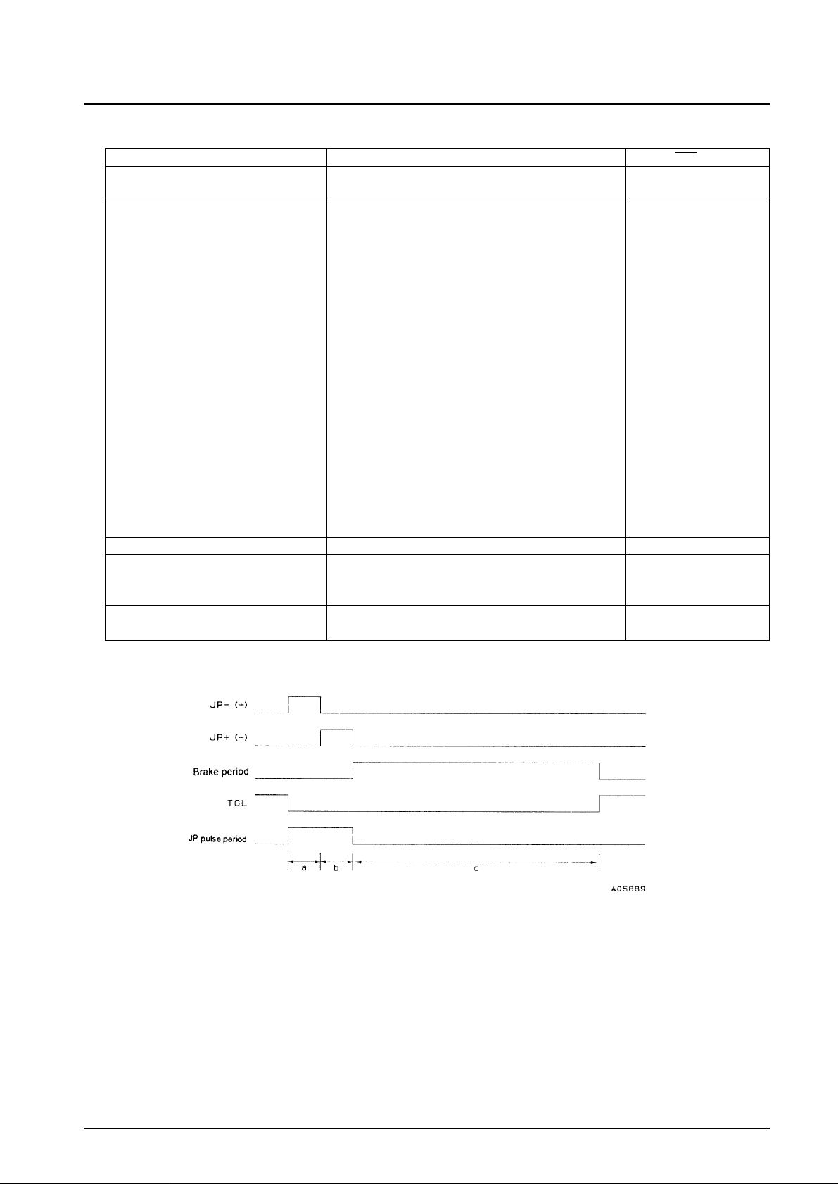
When the LC78622E receives a track jump instruction as a servo command, it first generates accelerating pulses
(period a) and next generates deceleration pulses (period b). The passage of the braking period (period c) completes
the specified jump. During the braking period, the LC78622E detects the beam slip direction from the TES and
HFL inputs. TOFF is used to cut the components in the TES signal that aggravate slip. The jump destination track
is captured by increasing the servo gain with TGL. In during TOFF output mode JP pulse period the TOFF signal
is held high during the JP pulse generation period.
Note: Of the modes related to disk motor control, the TOFF pin only goes low in CLV mode, and will be high
during accelerate, stop, and decelerate modes.Note that the TOFF pin can be turned on and off
independently by microprocessor issued commands. However, this function is only valid when disk motor
control is in CLV mode.
MSB LSB Command RES = low
1 0 1 0 0 0 0 0 STANDARD TRACK JUMP
●●
1 0 1 0 0 0 0 1 NEW TRACK JUMP
0 0 0 1 0 0 0 1 1 TRACK JUMP IN #1
0 0 0 1 0 0 1 0 1 TRACK JUMP IN #2
0 0 1 1 0 0 0 1 1 TRACK JUMP IN #3
0 1 0 1 0 0 1 0 1 TRACK JUMP IN #4
0 0 0 1 0 0 0 0 2 TRACK JUMP IN
0 0 0 1 0 0 1 1 4 TRACK JUMP IN
0 0 0 1 0 1 0 0 16 TRACK JUMP IN
0 0 1 1 0 0 0 0 32 TRACK JUMP IN
0 0 0 1 0 1 0 1 64 TRACK JUMP IN
0 0 0 1 0 1 1 1 128 TRACK JUMP IN
0 0 0 1 1 0 0 1 1 TRACK JUMP OUT #1
0 0 0 1 1 0 1 0 1 TRACK JUMP OUT #2
0 0 1 1 1 0 0 1 1 TRACK JUMP OUT #3
0 1 0 1 1 0 1 0 1 TRACK JUMP OUT #4
0 0 0 1 1 0 0 0 2 TRACK JUMP OUT
0 0 0 1 1 0 1 1 4 TRACK JUMP OUT
0 0 0 1 1 1 0 0 16 TRACK JUMP OUT
0 0 1 1 1 0 0 0 32 TRACK JUMP OUT
0 0 0 1 1 1 0 1 64 TRACK JUMP OUT
0 0 0 1 1 1 1 1 128 TRACK JUMP OUT
0 0 0 1 0 1 1 0 256 TRACK CHECK
0 0 0 0 1 1 1 1 TOFF
1 0 0 0 1 1 1 1 TON
●●
1 0 0 0 1 1 0 0 TRACK JUMP BRAKE
0 0 1 0 0 0 0 1 TOFF OUTPUT MODE DURING JP PULSE PERIOD
0 0 1 0 0 0 0 0 RESET TOFF OUTPUT MODE DURING JP PULSE PERIOD
●●
Page 15
No. 5480-15/29
LC78622E
• Track jump modes
The table lists the relationships between acceleration pulses (the a period) , deceleration pulses (the b period), and
the braking period (the c period).
Note: 1. As indicated in the table, actuator signals are not output during the 256 TRACK CHECK function. This is a mode in which the TES signal is counted
in the tracking loop off state. Therefore, feed motor forwarding is required.
2. The servo command register is automatically reset after one cycle of the track jump sequence (a, b, c) completes.
3. If another track jump command is issued during a track jump operation, the content of that new command will be executed starting immediately.
4. The 1 TRACK JUMP #3 mode does not have a braking period (the C period). Since brake mode must be generated by an external circuit, care is
required when using this mode.
5. While there was no braking period (the C period) in the LC78620E/21E for the new track jump command “2 TRACK JUMP IN (OUT)”, this has been
changed in this LSI, which has a C period of 60 ms.
The THLD signal is generated by the LA9230M, LA9231M, or LA9240M, and the tracking signal is held during the JP pulse period.
Standard track jump mode New track jump mode
Command
a b c a b c
1 TRACK JUMP IN (OUT) #1 233 µs 233 µs 60 ms 233 µs 233 µs 60 ms
1 TRACK JUMP IN (OUT) #2
0.5 track
233 µs 60 ms
0.5 track The same
60 ms
jump period jump period time as “a”
1 TRACK JUMP IN (OUT) #3
0.5 track
233 µs
This period does 0.5 track The same This period does
jump period not exist. jump period time as “a” not exist.
0.5 track
60 ms; TOFF is
0.5 track The same
60 ms; TOFF is
1 TRACK JUMP IN (OUT) #4
jump period
233 µs low during
jump period time as “a”
low during
the C period. the C period.
2 TRACK JUMP IN (OUT) None None None
1 track The same
60 ms
jump period time as “a”
4 TRACK JUMP IN (OUT)
2 track
466 µs 60 ms
2 track The same
60 ms
jump period jump period time as “a”
16 TRACK JUMP IN (OUT)
9 track 7 track
60 ms
9 track The same
60 ms
jump period jump period jump period time as “a”
32 TRACK JUMP IN (OUT)
18 track 14 track
60 ms
18 track 14 track
60 ms
jump period jump period jump period jump period
64 TRACK JUMP IN (OUT)
36 track 28 track
60 ms
36 track 28 track
60 ms
jump period jump period jump period jump period
128 TRACK JUMP IN (OUT)
72 track 56 track
60 ms
72 track 56 track
60 ms
jump period jump period jump period jump period
TOFF goes high during the period TOFF goes high during the period
256 TRACK CHECK when 256 tracks are passed over. 60 ms when 256 tracks are passed over. 60 ms
The a and b pulses are not output. The a and b pulses are not output.
TRACK JUMP BRAKE There are no a or b periods. 60ms There are no a and b periods. 60 ms
Page 16
No. 5480-16/29
LC78622E
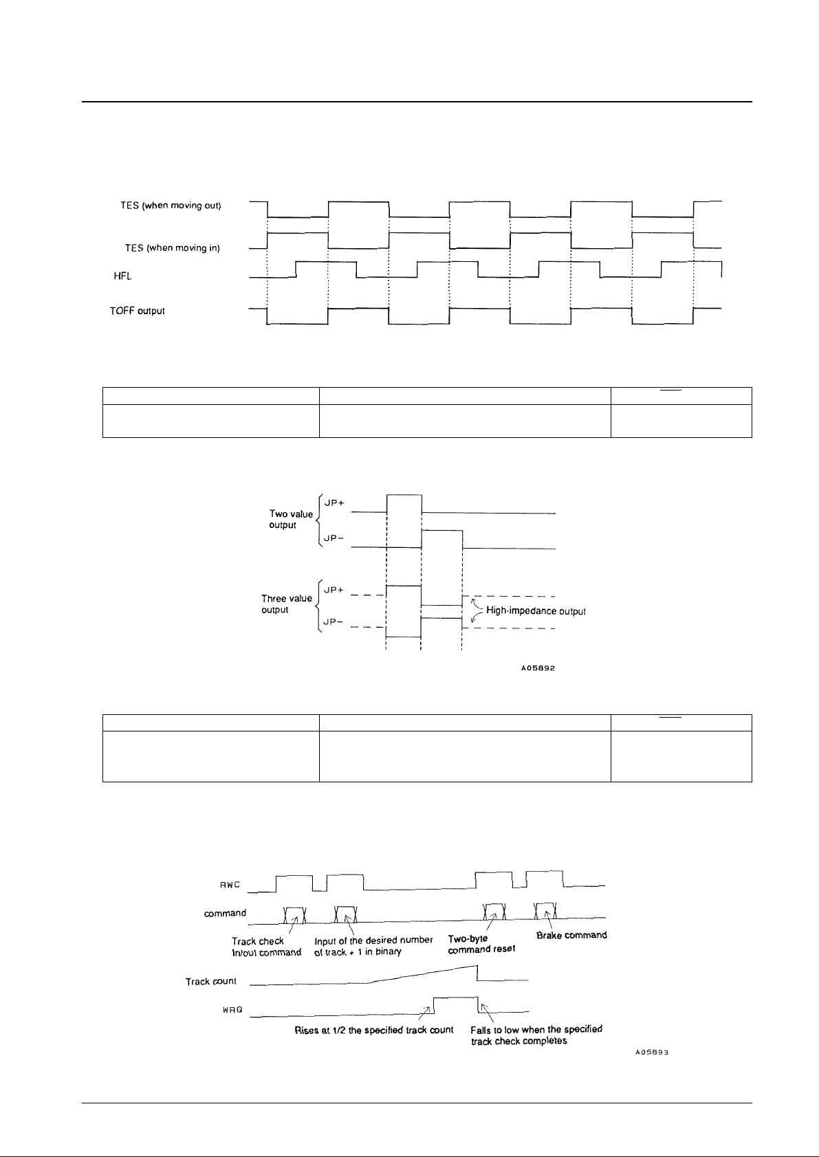
5. Tracking brake
The chart shows the relationships between the TES, HFL, and TOFF signals during the track jump C period. The TOFF signal is extracted from the
HFL signal by TES signal edges. When the HFL signal is high, the pickup is over the mirror surface, and when low, the pickup is over data bits.
Thus braking is applied based on the TOFF signal being high when the pickup is moving from a mirror region to a data region and being low when
the pickup is moving from a data region to a mirror region.
• JP three-value output
The JP three-value output command allows the track jump operation to be controlled from a single pin.
• Track check mode
The LC78622E will count the specified number of tracks minus one when the microprocessor sends an arbitrary
binary value in the range 8 to 254 after issuing either a track check in or a track check out command.
MSB LSB Command RES = low
1 0 1 1 0 1 1 0 JP THREE VALUE OUTPUT
1 0 1 1 0 1 1 1 JP TWO VALUE OUTPUT (earlier scheme)
●●
MSB LSB Command RES = low
1 1 1 1 0 0 0 0 TRACK CHECK IN
1 1 1 1 1 0 0 0 TRACK CHECK OUT
1 1 1 1 1 1 1 1 TWO BYTE COMMAND RESET
●●
Page 17
No. 5480-17/29
LC78622E
Note: 1. When the desired track count has been input in binary, the track check operation is started by the fall of RWC.
2. During a track check operation the TOFF pin goes high and the tracking loop is turned off. Therefore, feed motor forwarding is required.
3. When a track check in/out command is issued the function of the WRQ signal switches from the normal mode subcode Q standby monitor function
to the track check monitor function. This signal goes high when the track check is half completed, and goes low when the check finishes. The
control microprocessor should monitor this signal for a low level to determine when the track check completes.
4. If a two-byte reset command is not issued, the track check operation will repeat. That is, to skip over 20,000 tracks, issue a track check 201
command once, and then count the WRQ signal 100 times. This will check 20,000 tracks.
5. After performing a track check operation, use the brake command to have the pickup lock onto the track.
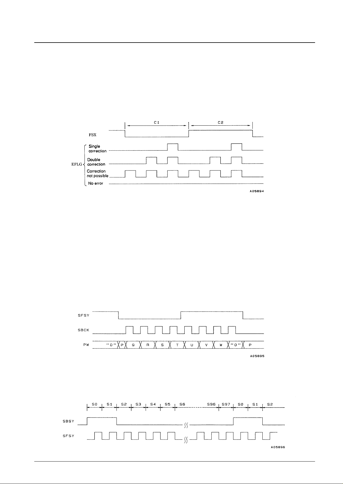
8. Error Flag Output; Pin 48: EFLG, pin 52: FSX
The FSX signal is generated by dividing the crystal oscillator clock, and is a 7.35 kHz frame synchronization signal.
The error correction state for each frame is output from EFLG. The FSX low-level period indicates the C1 correction
state, and the high-level period indicates the C2 correction state. The playback OK/NG state can be easily determined
from the extent of the high level that appears here.
9. Subcode P, Q and R to W Output Circuit; Pin 49: PW, pin 47: SBSY, pin 50: SFSY, pin 51: SBCK
PW is the subcode signal output pin, and all the codes, P, Q, and R to W can be read out by sending eight clocks to
the SBCK pin within 136 µs after the fall of SFSY. The signal that appears on the PW pin changes on the rising edge
of SBCK. If a clock is not applied to SBCK, the P code will be output from PW. SFSY is a signal that is output for
each subcode frame cycle, and the falling edge of this signal indicates standby for the output of the subcode symbol
(P to W). Subcode data P is output on the fall of this signal.
SBSY is a signal output for each subcode block. This signal goes high for the S0 and S1 synchronization signals. The
fall of this signal indicates the end of the subcode synchronization signals and the start of the data in the subcode
block. (EIAJ format)
Page 18
No. 5480-18/29
LC78622E
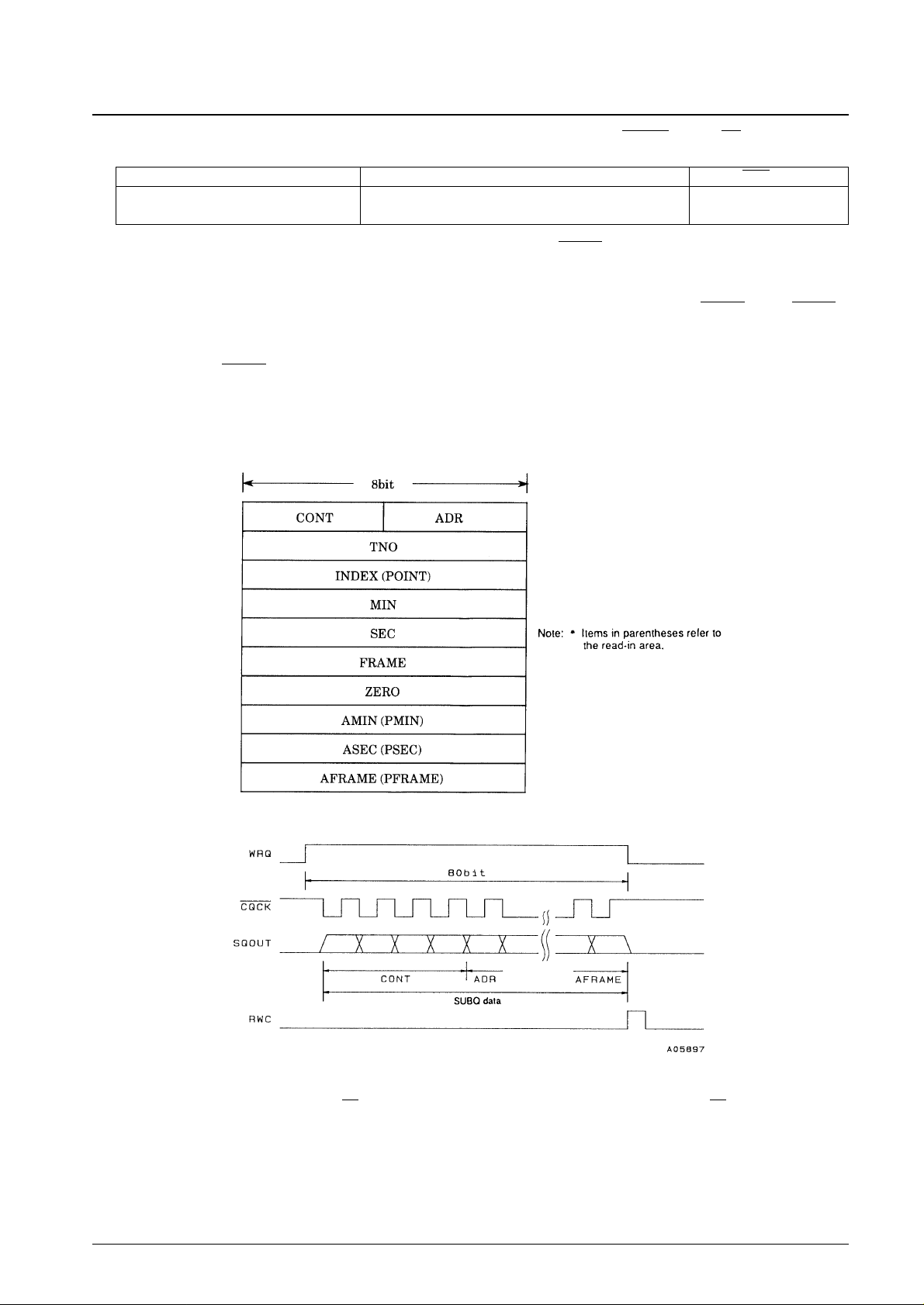
10. Subcode Q Output Circuit; Pin 53: WRQ, pin 54: RWC, pin 55: SQOUT, pin 57: CQCK, pin 63: CS
Subcode Q can be read from the SQOUT pin by applying a clock to the CQCKpin.
Of the eight bits in the subcode, the Q signal is used for song (track) access and display. The WRQ will be high only if
the data passed the CRC error check and the subcode Q format internal address is 1*. The control microprocessor can
read out data from SQOUT in the order shown below by detecting this high level and applying CQCK. When CQCK
is applied the DSP disables register update internally. The microprocessor should give update permission by setting
RWC high briefly after reading has completed. WRQ will fall to low at this time. Since WRQ falls to low 11.2 ms
after going high, CQCK must be applied during the high period. Note that data is read out in an LSB first format.
Note: * That state will be ignored if an address free command is input. This is provided to handle CD-ROM
applications.
Note: 1. Normally, the WRQ pin indicates the subcode Q standby state. However, it is used for a different monitoring purpose in track check mode and
during internal braking. (See the items on track counting and internal braking for details.)
2. The LC78622E becomes active when the CS pin is low, and subcode Q data is output from the SQOUT pin. When the CS pin is high, the SQOUT
pin goes to the high-impedance state.
MSB LSB Command RES = low
0 0 0 0 1 0 0 1 ADDRESS FREE
1 0 0 0 1 0 0 1 ADDRESS 1
●●
Page 19
No. 5480-19/29
LC78622E
11. Bilingual Function
• Following a reset or when a stereo (28H) command has been issued, the left and right channel data is output to the
left and right channels respectively.
• When an Lch set (29H) command is issued, the left and right channels both output the left channel data.
• When an Rch set (2AH) command is issued, the left and right channels both output the right channel data.
12. De-Emphasis; Pin 29: EMPH
The preemphasis on/off bit in the subcode Q control information is output from the EMPH pin. When this pin is
high, the LC78622E internal de-emphasis circuit operates and the digital filters and the D/A converter output deemphasized data.
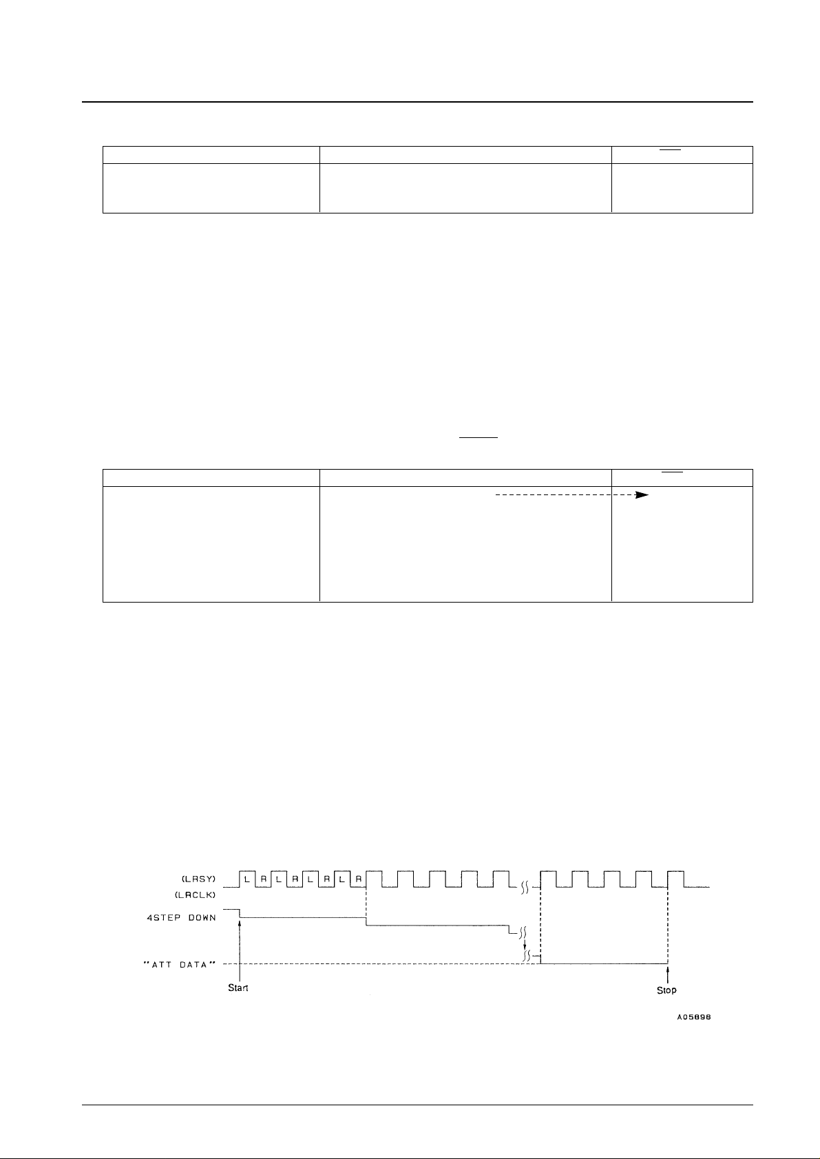
13. Digital Attenuator
Digital attenuation can be applied to the audio data by setting the RWC pin high and inputting the corresponding
two-byte command to the COIN pin in synchronization with the CQCK clock.
• Attenuation setup
Since the attenuation level is set to the muted state (a muting of –∞ is specified by an attenuation coefficient of
00H) after the attenuation level is reset, the attenuation coefficient must be directly set to EEH (using the ATT
DATA SET command) to output audio signals. Note that the attenuation level can be set to one of 239 values from
00H to EEH.
These two-byte commands differ from the two-byte commands used for track counting in that it is only necessary
to set RWC once and a two-byte command reset is not required. After inputting the target attenuation level as a
value in the range 00H to EEH, sending an attenuator step up/down command will cause the attenuation level to
approach the target value in steps of 4, 8, or 16 units as specified in synchronization with rising edges on the LRSY
input. However, the ATT DATA SET command sets the target value directly. If a new data value is input during
the transition, the value begins to approach the new target value at that point. Note that the UP/DOWN distinction
is significant here.
MSB LSB Command RES = low
0 0 1 0 1 0 0 0 STO CONT
●●
0 0 1 0 1 0 0 1 Lch CONT
0 0 1 0 1 0 1 0 Rch CONT
MSB LSB Command RES = low
1 0 0 0 0 0 0 1 ATT DATA SET DATA 00H set
1 0 0 0 0 0 1 0 ATT 4 STEP UP
(MUTE –∞ dB)
1 0 0 0 0 0 1 1 ATT 4 STEP DOWN
1 0 0 0 0 1 0 0 ATT 8 STEP UP
1 0 0 0 0 1 0 1 ATT 8 STEP DOWN
1 0 0 0 0 1 1 0 ATT 16 STEP UP
1 0 0 0 0 1 1 1 ATT 16 STEP DOWN
Page 20
No. 5480-20/29
LC78622E
Audio output level = 20 log [dB]
For example, the formula below calculates the time required for the attenuation level to increase from 00H to EEH
when a 4STEP UP command is executed. Note that the control microprocessor must provide enough of a time
margin for this operation to complete before issuing the next attenuation level set command.
≈ 21.6 ms
Note: Setting the attenuation level to values of EFH or higher is disallowed to prevent overflows in one-bit D/A
converter calculations from causing noise.
14. Mute Output; Pin 35: MUTEL, pin 42: MUTER
15. C2 Flag Output; Pin 30: C2F
C2F output flag information in 8-bit units.
16. Digital Output Circuit; Pin 31: DOUT
This is an output pin for use with a digital audio interface. Data is output in the EIAJ format. This signal has been
processed by the interpolation and muting circuits. This pin has a built-in driver circuit and can directly drive a
transformer.
• The DOUT pin can be locked at the low level by issuing a DOUT OFF command.
• The UBIT information in the DOUT data can be locked at zero by issuing a UBIT OFF command.
• The DOUT data can be switched to data for which interpolation and muting processing have not been performed
by issuing a CD-ROM XA command.
17. Mute Control Circuit
Inputting the above command mutes the audio level (MUTE -∞ dB). Since zero-cross muting is used, there is very
little noise associated with this operation. The IC defines zero cross to be the ranges where the upper 7 bits of the
data are all zeros or all ones. Note that the MUTE -12 dB instruction supported by the LC78620E has been removed
from this product.
238 level × 4STEP UP
44.1 kHz
ATT DATA
MSB LSB Command RES = low
0 1 0 0 0 0 1 0 DOUT ON
●●
0 1 0 0 0 0 1 1 DOUT OFF
0 1 0 0 0 0 0 0 UBIT ON
●●
0 1 0 0 0 0 0 1 UBIT OFF
1 0 0 0 1 0 0 0 CDROM-XA
1 0 0 0 1 0 1 1 ROMXA-RST
●●
MSB LSB Command RES = low
0 0 0 0 0 0 0 1 MUTE: 0 dB
0 0 0 0 0 0 1 1 MUTE: –∞ dB
●●
Page 21
No. 5480-21/29
LC78622E
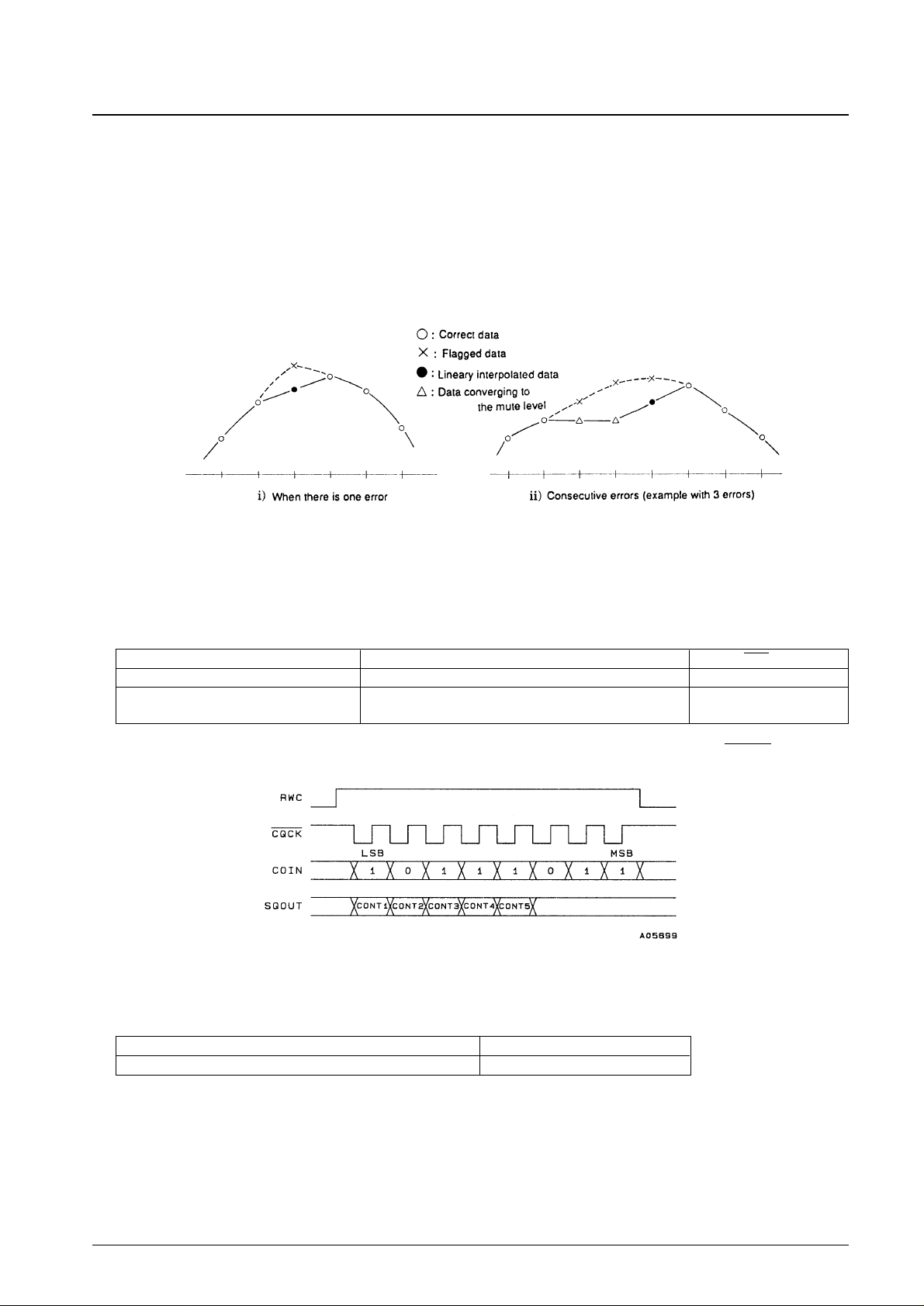
18. Interpolation Circuit
Outputting incorrect audio data that could not be corrected by the error detection and correction circuit would result
in loud noises being output. To minimize this noise, the LC78622E replaces the incorrect data with linearly
interpolated data based on the correct data on either side of the incorrect data. If one set of C2 flags indicate errors,
the above replacement is performed, and if two or more sets of C2 flags indicate errors, the IC holds the previous
value. However, when correct data is output following two or more consecutive C2 flags indicating errors, the data
point between the correct data and the data output two points previously (the held value) is replaced with a value
computed by linearly interpolating those two values.
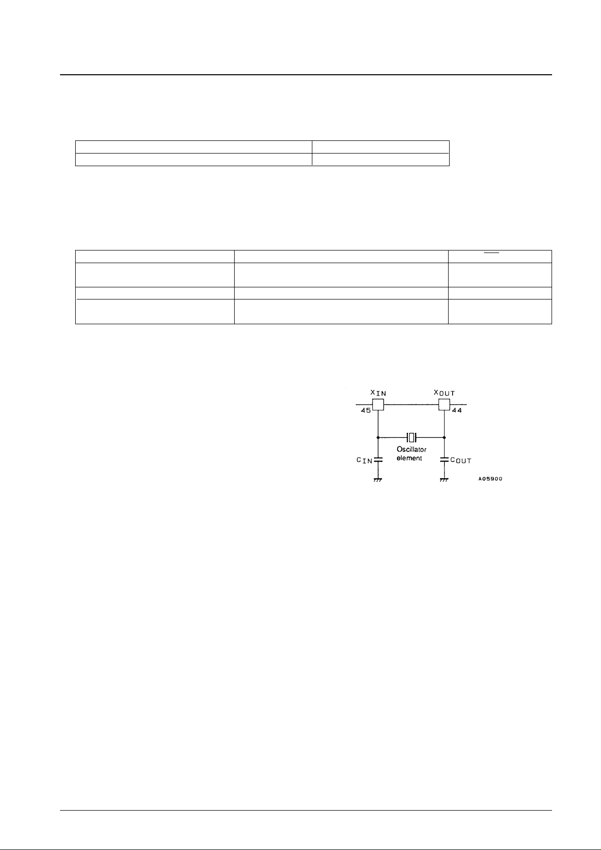
19. General-Purpose I/O Ports; Pin 24: CONT1, Pin 25: CONT2, Pin 26: CONT3, Pin 27: CONT4, Pin 28: CONT5
The LC78622E provides the five CONT1 to CONT5 I/O ports. These are all set to function as input pins after a reset.
Unused port pins should be either connected to ground or set to the output port function.
Port data is read in by the PORT READ command in synchronization with the falling edge of the CQCK pin by the
SQOUT pin in the order CONT1 to CONT5. This command is a single-byte command.
Additionally, these ports can be set up individually to function as control output pins with the PORT OP-E/D SET
command. The ports are selected using the lower 5 bits of the 1Byte data. The bits in the data correspond to CONT1
to CONT5 in order starting with the LSB of the 1Byte data. This command is a Two- byte command. (RWC set
once)
dn =1
...
Sets CONTn to be an output pin
dn =0
...
Sets CONTn to be an input pin
X
... don’t care
MSB LSB Command RES = low
1 1 0 1 1 1 0 1 PORT READ
1 1 0 1 1 0 1 1 PORT OP-E/D SET PORT I SET
1 1 0 1 1 1 0 0 PORT DATA SET
MSB LSB Command
1 1 0 1 1 0 1 1 X X X d5 d4 d3 d2 d1 PORT OP-E/D SET
Page 22
No. 5480-22/29
LC78622E
Ports set to be output pins can output high or low levels independently. The lower 5 bits of the 1 Byte data
correspond to those ports. The bits in the data correspond to CONT1 to CONT5 in order starting with the LSB of the
1 Byte data. This command is a two-byte command. (RWC set once)
dn =1
...
Sets CONTn to be an output pin
dn =0
...
Sets CONTn to be an input pin
X
... don’t care
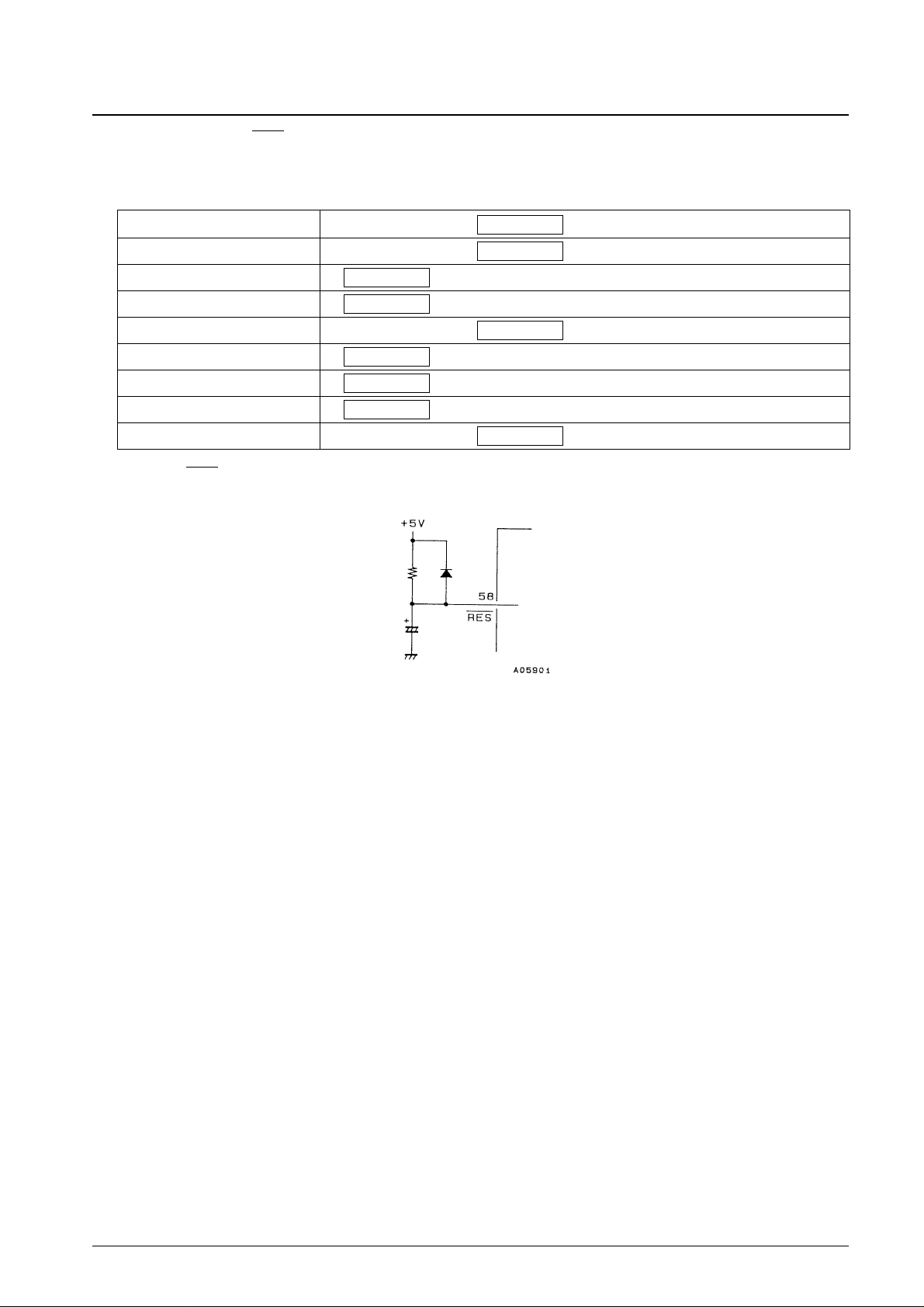
20. Clock Oscillator; Pin 45: XIN, pin 44: X
OUT
21. 16M and 4.2M Pins; Pin 60: 16M, pin 61: 4.2M
Both in normal- and double-speed playback modes, the 16M pin buffer outputs the 16.9344 MHz external crystal
oscillator 16.9344 MHz signal. The 4.2M pin supplies the LA9230M, LA9231M or LA9240M system clock, normally
outputting a 4.2336 MHz signal. When the oscillator is turned off both these pins will be fixed at either high or low.
MSB LSB Command RES = low
1 0 0 0 1 1 1 0 OSC ON
●●
1 0 0 0 1 1 0 1 OSC OFF
1 1 0 0 1 1 1 0 XTAL 16M
●●
1 1 0 0 0 0 1 0 NORMAL-SPEED PLAYBACK ●●
1 1 0 0 0 0 0 1 DOUBLE-SPEED PLAYBACK
The clock that is used as the time base is generated by connecting a 16.9344 MHz oscillator element between these
pins. The OSC OFF command turns off both the VCO and crystal oscillators. The system control microprocessor can
issue double-speed or normal-speed playback command when the application implements double-speed playback
system.
MSB LSB Command
1 1 0 1 1 1 0 0 X X X d5 d4 d3 d2 d1 PORT DATA SET
Page 23
No. 5480-23/29
LC78622E
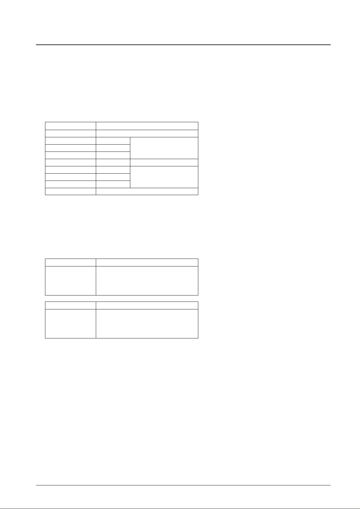
22. Reset Circuit; Pin 58: RES
When power is first applied, this pin should be briefly set low and then set high. This will set the muting to –∞ dB
and stop the disk motor.
Setting the RES pin low sets the LC78622E to the settings enclosed in boxes in the table.
23. Other Pins; Pin 2:TAI, pin 64: TEST1, pin 11: TEST2, pin 32: TEST3, pin 33: TEST4, pin 62: TEST5, pin 59:
TST11
These pins are used for testing the LSI’s internal circuits. Even though pull-down resistors are built into the TAI and
TEST2 to TEST5 input pin circuits, these pins must be connected to 0 V during normal operation. TST11 is an output
pin and should normally be left open.
Constant linear velocity servo START BRAKE CLV
Muting control 0 dB
Q subcode address conditions Address free
Track jump mode New
Track count mode Standard
Digital attenuator DATA 00H to EEH
OSC OFF
Playback speed Double speed
Digital filter normal speed ON
OFF
Normal speed
ON
DATA 0
New
Standard
Address 1
–∞
STOP
Page 24
No. 5480-24/29
LC78622E
24. Circuit Block Operating Descriptions
• RAM address control
The LC78622E incorporates an 8-bit × 2k-word RAM on chip. This RAM has an EFM demodulated data jitter
handling capacity of ±4 frames implemented using address control. The LC78622E continuously checks the remaining
buffer capacity and controls the data write address to fall in the center of the buffer capacity by making fine
adjustments to the frequency divisor in the PCK side of the CLV servo circuit. If the ±4 frame buffer capacity is
exceeded, the LC78622E forcibly sets the write address to the ±0 position. However, since the errors that occur due to
this operation cannot be handled with error flag processing, the IC applies muting to the output for a 128 frame period.
• C1 and C2 Error Correction
The LC78622E writes EFM demodulated data to internal RAM to compensate for jitter and then performs the
following processing with uniform timing based on the crystal oscillator clock. First, the LC78622E performs C1
error checking and correction in the C1 block, determines the C1 flags, and writes the C1 flag register. Next, the
LC78622E performs C2 error checking and correction in the C2 block, determines the C2 flags, and writes data to
internal RAM.
Note: 1. If the positions of the errors determined by the C2 check agree with those specified by the C1 flags, the correction is performed and the flags
are cleared. However, if the number of C1 flags is 7 or higher, C2 correction may fail. In this case correction is not performed and the C1 flags
are taken as the C2 flags without change. Error correction is not possible if one error position agrees and the other does not. Furthermore, if
the number of C1 flags is 5 or under, the C1 check result can be seen as unreliable. Accordingly, the flags will be set in this case. Cases
where the number of C1 flags is 6 or more are handled in the same way, and the C1 flags are taken as the C2 flags without change. When
there is not even one agreement between the error positions, error correction is, of course, impossible. Here, if the number of C1 flags was 2
or under, data that was seen as correct after C1 correction is now seen as incorrect data. The flags are set in this case. In other cases, the C1
flags are taken as the C2 flags without change.
2. When data is determined to have three or more errors and be uncorrectable, correction is, of course, impossible. Here, if the number of C1
flags was 2 or under, data that was seen as correct after C1 correction is now seen as incorrect data. The flags are set in this case. In other
cases the C1 flags are taken as the C2 flags without change
Position Division ratio or processing
–4 or less Force to ±0
–3 589
–2 589 Increase ratio
–1 589
±0 588 Standard ratio
+1 587
+2 587 Decrease ratio
+3 587
+4 or more Force to ±0
C1 flag Error correction and flag processing
No errors No correction required · Flag reset
1 error Correction · Flag reset
2 errors Correction · Flag set
3 errors or more Correction not possible · Flag set
C2 flag Error correction and flag processing
No errors No correction required · Flag reset
1 error Correction · Flag reset
2 errors Depends on C1 flags
*1
3 errors or more Depends on C1 flags
*2
Page 25
No. 5480-25/29
LC78622E
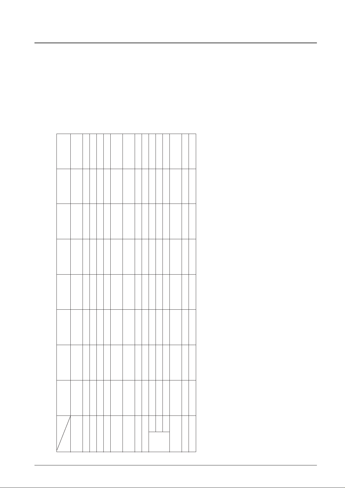
25. Command Summary Table
Blank entry: Illegal command, #: Changed or added command, *: Latching commands (mode setting commands),
●●: Commands shared with an ASP (LA9220M/30M/31M or other processor), Items in parentheses are ASP commands
(provided for reference purposes)
0 0 0 0 0 0 0 0 (ADJ.reset) 0 0 1 0 0 0 0 0 * TOFF low in 0 1 0 0 0 0 0 0 * UBIT ON 0 1 1 0 0 0 0 0
TJ mode
0 0 0 0 0 0 0 1 * MUTE 0 dB 0 0 1 0 0 0 0 1 * TOFF high in 0 1 0 0 0 0 0 1 * UBIT OFF 0 1 1 0 0 0 0 1
TJ mode
0 0 0 0 0 0 1 0 # 0 0 1 0 0 0 1 0 * New TRACK 0 1 0 0 0 0 1 0 * DOUT ON 0 1 1 0 0 0 1 0
COUNT
0 0 0 0 0 0 1 1 * MUTE –∞ dB 0 0 1 0 0 0 1 1 * Old TRACK 0 1 0 0 0 0 1 1 * DOUT OFF 0 1 1 0 0 0 1 1
COUNT
0 0 0 0 0 1 0 0 * DISC MTR START 0 0 1 0 0 1 0 0 0 1 0 0 0 1 0 0 0 1 1 0 0 1 0 0
0 0 0 0 0 1 0 1 * DISC MTR CLV 0 0 1 0 0 1 0 1 0 1 0 0 0 1 0 1 0 1 1 0 0 1 0 1
0 0 0 0 0 1 1 0 * DISC MTR BRAKE 0 0 1 0 0 1 1 0 0 1 0 0 0 1 1 0 0 1 1 0 0 1 1 0
0 0 0 0 0 1 1 1 * DISC MTR STOP 0 0 1 0 0 1 1 1 0 1 0 0 0 1 1 1 0 1 1 0 0 1 1 1
0 0 0 0 1 0 0 0 ●● FOCUS START 0 0 1 0 1 0 0 0 * STO CONT 0 1 0 0 1 0 0 0 0 1 1 0 1 0 0 0
#1
0 0 0 0 1 0 0 1 * ADDRESS FREE 0 0 1 0 1 0 0 1 * LCH CONT 0 1 0 0 1 0 0 1 0 1 1 0 1 0 0 1
0 0 0 0 1 0 1 0 # 0 0 1 0 1 0 1 0 * RCH CONT 0 1 0 0 1 0 1 0 0 1 1 0 1 0 1 0
0 0 0 0 1 0 1 1 0 0 1 0 1 0 1 1 # 0 1 0 0 1 0 1 1 0 1 1 0 1 0 1 1 #
0 0 0 0 1 1 0 0 0 0 1 0 1 1 0 0 # 0 1 0 0 1 1 0 0 0 1 1 0 1 1 0 0 #
0 0 0 0 1 1 0 1 0 0 1 0 1 1 0 1 # 0 1 0 0 1 1 0 1 0 1 1 0 1 1 0 1
0 0 0 0 1 1 1 0 # 0 0 1 0 1 1 1 0 # 0 1 0 0 1 1 1 0 0 1 1 0 1 1 1 0 *DF normal speed
off
0 0 0 0 1 1 1 1 * TRACKING OFF 0 0 1 0 1 1 1 1 0 1 0 0 1 1 1 1 0 1 1 0 1 1 1 1 #
0 0 0 1 0 0 0 0 2TJ IN 0 0 1 1 0 0 0 0 32TJ IN 0 1 0 1 0 0 0 0 0 1 1 1 0 0 0 0
0 0 0 1 0 0 0 1 1TJ IN #1 0 0 1 1 0 0 0 1 1TJ IN #3 0 1 0 1 0 0 0 1 0 1 1 1 0 0 0 1
0 0 0 1 0 0 1 0 1TJ IN #2 0 0 1 1 0 0 1 0 0 1 0 1 0 0 1 0 1TJ IN #4 0 1 1 1 0 0 1 0
0 0 0 1 0 0 1 1 4TJ IN 0 0 1 1 0 0 1 1 0 1 0 1 0 0 1 1 0 1 1 1 0 0 1 1
0 0 0 1 0 1 0 0 16TJ IN 0 0 1 1 0 1 0 0 0 1 0 1 0 1 0 0 0 1 1 1 0 1 0 0
0 0 0 1 0 1 0 1 64TJ IN 0 0 1 1 0 1 0 1 0 1 0 1 0 1 0 1 0 1 1 1 0 1 0 1
0 0 0 1 0 1 1 0 256TC 0 0 1 1 0 1 1 0 0 1 0 1 0 1 1 0 0 1 1 1 0 1 1 0
0 0 0 1 0 1 1 1 128TJ IN 0 0 1 1 0 1 1 1 0 1 0 1 0 1 1 1 0 1 1 1 0 1 1 1
0 0 0 1 1 0 0 0 2TJ OUT 0 0 1 1 1 0 0 0 32TJ OUT 0 1 0 1 1 0 0 0 0 1 1 1 1 0 0 0
0 0 0 1 1 0 0 1 1TJ OUT #1 0 0 1 1 1 0 0 1 1TJ OUT #3 0 1 0 1 1 0 0 1 0 1 1 1 1 0 0 1
0 0 0 1 1 0 1 0 1TJ OUT #2 0 0 1 1 1 0 1 0 0 1 0 1 1 0 1 0 1TJ OUT #4 0 1 1 1 1 0 1 0
0 0 0 1 1 0 1 1 4TJ OUT 0 0 1 1 1 0 1 1 0 1 0 1 1 0 1 1 0 1 1 1 1 0 1 1
0 0 0 1 1 1 0 0 16TJ OUT 0 0 1 1 1 1 0 0 0 1 0 1 1 1 0 0 0 1 1 1 1 1 0 0
0 0 0 1 1 1 0 1 64TJ OUT 0 0 1 1 1 1 0 1 0 1 0 1 1 1 0 1 0 1 1 1 1 1 0 1
0 0 0 1 1 1 1 0 0 0 1 1 1 1 1 0 0 1 0 1 1 1 1 0 0 1 1 1 1 1 1 0
0 0 0 1 1 1 1 1 128TJ OUT 0 0 1 1 1 1 1 1 0 1 0 1 1 1 1 1 0 1 1 1 1 1 1 1
Continued on next page.
Page 26
No. 5480-26/29
LC78622E
Note: VCO × 2 SET command should be issued in case of low voltage power supply application.
Blank entry: Illegal command, #: Changed or added command, *: Latching commands (mode setting commands),
●●: Commands shared with an ASP (LA9220M/30M/31M or other processor), Items in parentheses are ASP commands
(provided for reference purposes)
1 0 0 0 0 0 0 0 1 0 1 0 0 0 0 0 * Old TRK JMP 1 1 0 0 0 0 0 0 1 1 1 0 0 0 0 0
1 0 0 0 0 0 0 1 * ATT DATA SET 1 0 1 0 0 0 0 1 * New TRK JMP 1 1 0 0 0 0 0 1 * Double-speed 1 1 1 0 0 0 0 1
playback
1 0 0 0 0 0 1 0 * ATT 4STP UP 1 0 1 0 0 0 1 0 FOCUS START #2 1 1 0 0 0 0 1 0 * Normal-speed 1 1 1 0 0 0 1 0
playback
1 0 0 0 0 0 1 1 * ATT 4STP DWN 1 0 1 0 0 0 1 1 * Internal BRAKE 1 1 0 0 0 0 1 1 1 1 1 0 0 0 1 1
CONT
1 0 0 0 0 1 0 0 * ATT 8STP UP 1 0 1 0 0 1 0 0 1 1 0 0 0 1 0 0 * Internal BRK OFF 1 1 1 0 0 1 0 0
1 0 0 0 0 1 0 1 * ATT 8STP DWN 1 0 1 0 0 1 0 1 1 1 0 0 0 1 0 1 * Internal BRK ON 1 1 1 0 0 1 0 1
1 0 0 0 0 1 1 0 * ATT 16STP UP 1 0 1 0 0 1 1 0 1 1 0 0 0 1 1 0 1 1 1 0 0 1 1 0
1 0 0 0 0 1 1 1 * ATT 16STP DWN 1 0 1 0 0 1 1 1 1 1 0 0 0 1 1 1 1 1 1 0 0 1 1 1
1 0 0 0 1 0 0 0 * #CDROMXA 1 0 1 0 1 0 0 0 * DISC 8 SET 1 1 0 0 1 0 0 0 # 1 1 1 0 1 0 0 0
1 0 0 0 1 0 0 1 * ADDRESS 1 1 0 1 0 1 0 0 1 * DISC 12 SET 1 1 0 0 1 0 0 1 *# 1 1 1 0 1 0 0 1
1 0 0 0 1 0 1 0 # 1 0 1 0 1 0 1 0 1 1 0 0 1 0 1 0 * Internal BRK-DMC 1 1 1 0 1 0 1 0
low
1 0 0 0 1 0 1 1 * #ROMXA 1 0 1 0 1 0 1 1 1 1 0 0 1 0 1 1 * Internal BRK-DMC 1 1 1 0 1 0 1 1
RST high
1 0 0 0 1 1 0 0 TRACK JMP BRK 1 0 1 0 1 1 0 0 #VCO X2 SET 1 1 0 0 1 1 0 0 * TOFF during 1 1 1 0 1 1 0 0
internal BRAKE
1 0 0 0 1 1 0 1 * OSC OFF 1 0 1 0 1 1 0 1 #VCO X1 SET 1 1 0 0 1 1 0 1 * TON during 1 1 1 0 1 1 0 1
internal BRAKE
1 0 0 0 1 1 1 0 * OSC ON 1 0 1 0 1 1 1 0 1 1 0 0 1 1 1 0 * Xtal 16M 1 1 1 0 1 1 1 0 * Command noise
rejecter OFF
1 0 0 0 1 1 1 1 * TRACKING ON 1 0 1 0 1 1 1 1 1 1 0 0 1 1 1 1 1 1 1 0 1 1 1 1 * Command noise
rejecter ON
1 0 0 1 0 0 0 0 (* F.OFF.ADJ.ST) 1 0 1 1 0 0 0 0 * CLV-PH 1/1 mode 1 1 0 1 0 0 0 0 1 1 1 1 0 0 0 0 * ●● TRCK CHECK
IN
(2BYTE DETECT)
1 0 0 1 0 0 0 1 (* F.OFF.ADJ.OFF) 1 0 1 1 0 0 0 1 * CLV-PH 1/2 mode 1 1 0 1 0 0 0 1 1 1 1 1 0 0 0 1
1 0 0 1 0 0 1 0 (* T.OFF.ADJ.ST) 1 0 1 1 0 0 1 0 * CLV-PH 1/4 mode 1 1 0 1 0 0 1 0 1 1 1 1 0 0 1 0
1 0 0 1 0 0 1 1 (* T.OFF.ADJ.OFF) 1 0 1 1 0 0 1 1 * CLV-PH 1/8 mode 1 1 0 1 0 0 1 1 1 1 1 1 0 0 1 1
1 0 0 1 0 1 0 0 (* LSR.ON) 1 0 1 1 0 1 0 0 * CLV3ST output ON 1 1 0 1 0 1 0 0 1 1 1 1 0 1 0 0
1 0 0 1 0 1 0 1 (* LSR.OF/F.SV.ON) 1 0 1 1 0 1 0 1 * CLV3ST output 1 1 0 1 0 1 0 1 1 1 1 1 0 1 0 1
OFF
1 0 0 1 0 1 1 0 (* LSR.OF/F.SV.OF) 1 0 1 1 0 1 1 0 * JP3ST output ON 1 1 0 1 0 1 1 0 1 1 1 1 0 1 1 0
1 0 0 1 0 1 1 1 (* SP.8CM) 1 0 1 1 0 1 1 1 * JP3ST output OFF 1 1 0 1 0 1 1 1 1 1 1 1 0 1 1 1
1 0 0 1 1 0 0 0 (* SP.12CM) 1 0 1 1 1 0 0 0 1 1 0 1 1 0 0 0 1 1 1 1 1 0 0 0 * ●● TRCK CHECK
OUT
(2BYTE DETECT)
1 0 0 1 1 0 0 1 (* SP.OFF) 1 0 1 1 1 0 0 1 1 1 0 1 1 0 0 1 1 1 1 1 1 0 0 1
1 0 0 1 1 0 1 0 (* SLED.ON) 1 0 1 1 1 0 1 0 1 1 0 1 1 0 1 0 1 1 1 1 1 0 1 0
1 0 0 1 1 0 1 1 (* SLED.OFF) 1 0 1 1 1 0 1 1 1 1 0 1 1 0 1 1 #PORT OP-ED SET 1 1 1 1 1 0 1 1
1 0 0 1 1 1 0 0 (* EF.BAL.START) 1 0 1 1 1 1 0 0 1 1 0 1 1 1 0 0 #PORT DATA SET 1 1 1 1 1 1 0 0
1 0 0 1 1 1 0 1 (* T.SERVO.OFF) 1 0 1 1 1 1 0 1 1 1 0 1 1 1 0 1 #PORT READ 1 1 1 1 1 1 0 1
1 0 0 1 1 1 1 0 (* T.SERVO.ON) 1 0 1 1 1 1 1 0 1 1 0 1 1 1 1 0 1 1 1 1 1 1 1 0 ●● NOTHING
1 0 0 1 1 1 1 1 1 0 1 1 1 1 1 1 1 1 0 1 1 1 1 1 1 1 1 1 1 1 1 1 * ●● 2BYTE CMD
RST
Continued from preceding page.
Page 27
No. 5480-27/29
LC78622E
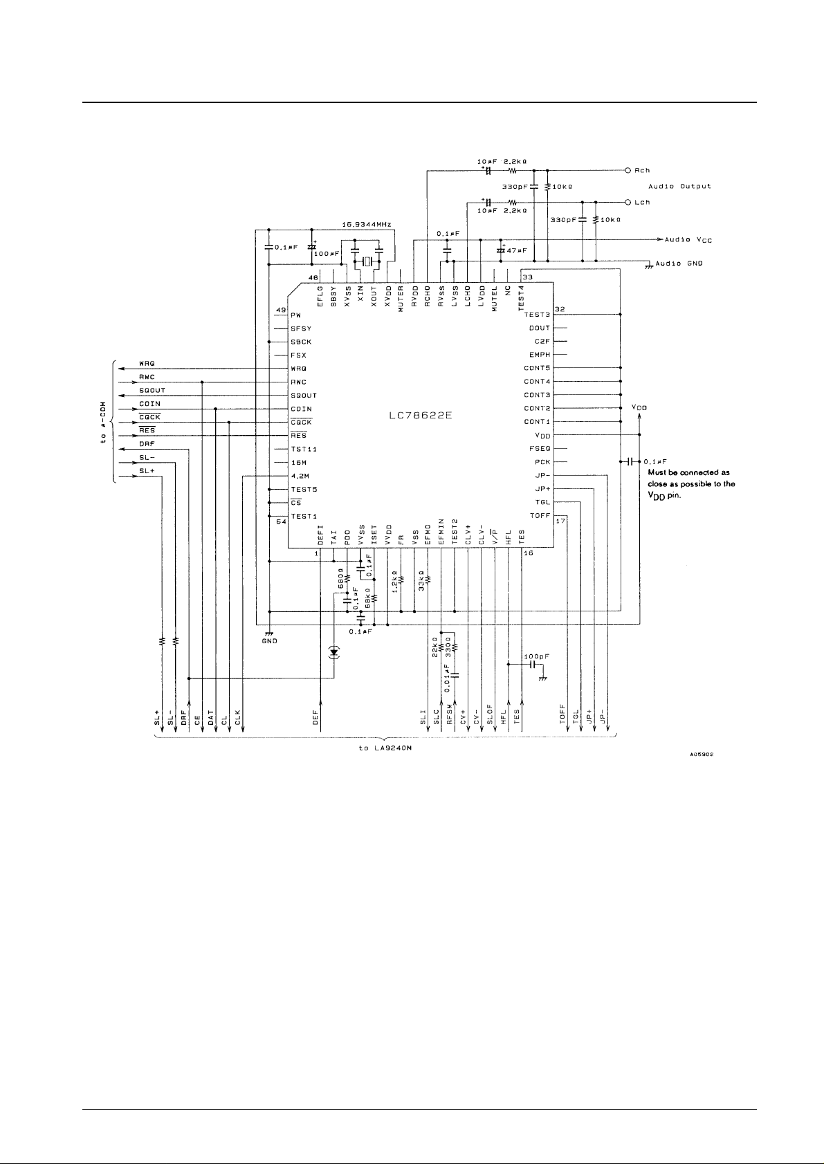
26. Sample Application Circuit
Page 28
No. 5480-28/29
LC78622E
27. CD-DSP Functional Comparison
Product
LC7860KA
LC7861NE→
LC7867E
LC7868E →
LC7869E
LC78681E →
LC78620E LC78622E
Function
LC7861KE LC7868KE LC78681KE
EFM-PLL
When paired with When paired with When paired with When paired with When paired with When paired with
Built-in VCO Built-in VCO
an analog ASP an analog ASP an analog ASP an analog ASP an analog ASP an analog ASP
16 KRAM External ●● ●● ●● ●● ●● ●● ●●
Speed st 2
✕/4✕ 2✕ st/4✕ st 2✕/4✕ 2✕ 2✕
Digital output ✕ ●● ●● ●● ●● ●● ●● ●●
Interpolation 2 4 4 4 4 4 4 2
Zero-cross
✕ ●● ●● ●● ●● ●● ●● ●●
muting
Level meter
✕ ✕ ✕ ●● ●● ●● ●●
✕
peak search
Bilingual ✕ ✕ ✕ ●● ●● ●● ●● ●●
Digital attenuator ✕ ✕ ✕ ✕ ✕ ✕ ●● ●●
Digital
2fs ●● ●● — — — — — —
filters
4fs — — — ●● — — — ●●
8fs — — — — ●● — ●● —
Digital
✕ ✕ ✕ ●● ●● ✕ ●● ●●
de-emphasis
1 bit D/A converter ✕ ✕ ✕ ✕ ✕ ✕ ●● ●●
Lowpass filter ✕ ✕ ✕ ✕ ✕ ✕ ✕ ●●
Page 29

No. 5480-29/29
LC78622E
This catalog provides information as of December, 1997. Specifications and information herein are subject to
change without notice.
■ No products described or contained herein are intended for use in surgical implants, life-support systems, aerospace
equipment, nuclear power control systems, vehicles, disaster/crime-prevention equipment and the like, the failure of
which may directly or indirectly cause injury, death or property loss.
■ Anyone purchasing any products described or contained herein for an above-mentioned use shall:
➀ Accept full responsibility and indemnify and defend SANYO ELECTRIC CO., LTD., its affiliates, subsidiaries and
distributors and all their officers and employees, jointly and severally, against any and all claims and litigation and all
damages, cost and expenses associated with such use:
➁ Not impose any responsibility for any fault or negligence which may be cited in any such claim or litigation on
SANYO ELECTRIC CO., LTD., its affiliates, subsidiaries and distributors or any of their officers and employees
jointly or severally.
■ Information (including circuit diagrams and circuit parameters) herein is for example only; it is not guaranteed for
volume production. SANYO believes information herein is accurate and reliable, but no guarantees are made or implied
regarding its use or any infringements of intellectual property rights or other rights of third parties.
 Loading...