


Ordering number : EN*4999
93098HA (OT) / 83194TH (OT) No. 4999-1/9
LC78855KM
SANYO Electric Co.,Ltd. Semiconductor Bussiness Headquarters
TOKYO OFFICE Tokyo Bldg., 1-10, 1 Chome, Ueno, Taito-ku, TOKYO, 110-8534 JAPAN
Digital Audio D/A Converter
with Built-in Digital Filters
CMOS LSI
Any and all SANYO products described or contained herein do not have specifications that can handle
applications that require extremely high levels of reliability, such as life-support systems, aircraft’s
control systems, or other applications whose failure can be reasonably expected to result in serious
physical and/or material damage. Consult with your SANYO representative nearest you before using
any SANYO products described or contained herein in such applications.
SANYO assumes no responsibility for equipment failures that result from using products at values that
exceed, even momentarily, rated values (such as maximum ratings, operating condition ranges, or other
parameters) listed in products specifications of any and all SANYO products described or contained
herein.
Overview
The LC78855KM is a Σ∆ D/A converter with built-in
digital filters for use in digital audio products.
Features
•8×oversampling digital filters
• Digital de-emphasis (for Fs = 44.1 kHz)
• Digital attenuation (with serial input)
• Soft muting (with parallel inputs)
• Supports double-speed playback.
• Supports a 384 fs system clock.
• PWM output
• Single 5 V power supply
• Si gate CMOS process
Package Dimensions
unit: mm
3091-MFP28
Preliminary
Specifications
Absolute Maximum Ratings at Ta = 25°C
Allowable Operating Ranges at Ta = –30 to +75°C
Parameter Symbol Conditions Ratings Unit
Maximum supply voltage V
DD
max –0.3 to +7.0 V
Maximum input voltage V
IN
max –0.3 to VDD+ 0.3 V
Maximum output voltage V
OUT
max –0.3 to VDD+ 0.3 V
Operating temperature Topr –30 to +75 °C
Storage temperature Tstg –40 to +125 °C
Parameter Symbol Conditions min typ max Unit
Supply voltage V
DD
4.5 5.0 5.5 V
Input voltage range V
IN
0V
DD
V
[LC78855KM]
SANYO: MFP28
DC Characteristics at Ta = –30 to +75°C, VDD= 4.5 to 5.5 V, VSS= 0 V
AC Characteristics at Ta = –30 to +75°C, VDD= 4.5 to 5.5 V, VSS= 0 V
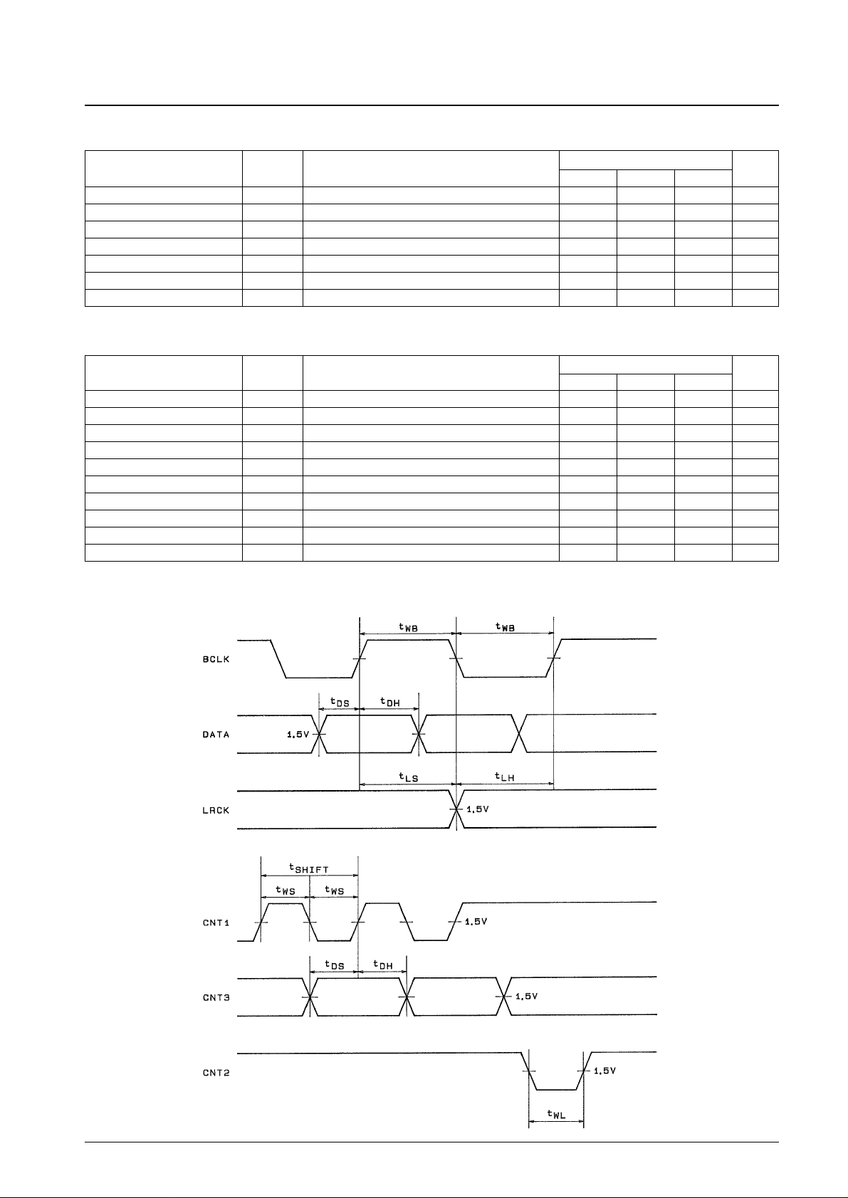
Timing Diagrams
No. 4999-2/9
LC78855KM
Parameter Symbol Conditions
Ratings
Unit
min typ max
Input high level voltage (1) V
IH
1 The XIN pin 0.7 V
DD
V
Input low level voltage (2) V
IL
1 The XIN pin 0.3 V
DD
V
Input high level voltage (1) V
IH
2 Pins other than the XIN pin 2.2 V
Input low level voltage (2) V
IL
2 Pins other than the XIN pin 0.8 V
Output high level voltage V
OHIOH
= –1 µA VDD– 0.1 V
Output low level voltage V
OLIOL
= 1 µA 0.1 V
Allowable power dissipation Pd V
DD
= 5.0 V 175 250 mW
Parameter Symbol Conditions
Ratings
Unit
min typ max
Oscillator frequency f
X
16.9 18.5 MHz
BCLK frequency f
BCX
2.4 MHz
BCLK pulse width t
WB
100 ns
Data setup time t
DS
20 ns
Data hold time t
DH
20 ns
LRCK setup time t
LS
50 ns
LRCK hold time t
LH
50 ns
CNT1 pulse period t
SHIFT
1000 ns
CNT1 pulse width t
WS
300 ns
CNT2 pulse width t
WL
300 ns

Analog Characteristics at Ta = 25°C, VDD= 5.0 V
Note: * For a 1 kHz, 0 dB input, measured in the circuit presented as a sample application circuit.
Block Diagram
Pin Assignment
No. 4999-3/9
LC78855KM
Parameter Symbol Conditions
Ratings
Unit
min typ max
Total harmonic distortion THD + N 1 kHz, 0 dB 0.01 %
Signal-to-noise ratio S/N JIS-A 93 dB
Crosstalk CT 1 kHz, 0 dB 80 dB
Full-scale output level VFS * 1.7 Vrms
Dynamic range DR JIS-A 83 dB

Pin Functions
LC78855KM Operation
The LC78855KM consists of two major sections; a digital filter block and a D/A converter.
1. Digital Filter Block
• Standard speed operation
The LC78855KM implements 8× oversampling using three filters: a 43rd order FIR filter, an 11th order FIR filter
and a third order FIR filter. De-emphasis is performed using a first order IIR filter.
• Double speed operation
This mode is used, for example, for dubbing a CD to a cassette at double speed. The XIN pin functions in the same
manner as in standard mode, but the BCLK, LRCK and DATA signals are input at twice the speed. After deemphasis is performed with a first order IIR filter 4× oversampling is performed using two filters: a 43rd order FIR
filter and a third order FIR filter.
No. 4999-4/9
LC78855KM
Pin No. Function Description
1 RESETB Reset input (Internal circuits are initialized when a low level is input to this pin.)
2 CNT1
When MODE = low: Control data shift clock
When MODE = high: Emphasis on/off switch
3 CNT2
When MODE = low: Control data latch signal input
When MODE = high: Standard speed/double speed switch
4 CNT3
When MODE = low: Control data input
When MODE = high: Soft muting input
5 BCLK Bit clock input
6 LRCK LR clock input
7 DATA Digital audio data input
8 MODE Serial/parallel input setting
9 CLKOUT Clock output
10 XV
DD
Oscillator amplifier power supply
11 XIN Oscillator amplifier input
12 XOUT Oscillator amplifier output
13 XGND Oscillator amplifier ground
14 DGND Digital system ground
15 MUTERO Right channel muting signal output
16 TEST Test pin (Must be tied low in normal operation.)
17 AV
DD
4 Analog system power supply
18 OUTRA Right channel output A
19 AGND2 Analog system ground
20 OUTRB Right channel output B
21 AV
DD
3 Analog system ground
22 AV
DD
2 Analog system ground
23 OUTLB Left channel output B
24 AGND1 Analog system ground
25 OUTLA Left channel output A
26 AV
DD
1 Analog system ground
27 MUTELO Left channel muting signal output
28 DV
DD
Digital system power supply

2. 1-Bit D/A Converter Block
The 1-bit D/A converter block takes the 8 Fs data input and outputs it as a 384 Fs 1-bit data series.
Input Settings
1. Input data format
2. Mode setting
• Serial input mode (MODE = low)
Attenuation data, de-emphasis on/off and the standard speed/double speed settings are input to the three lines
CNT1, CNT2 and CNT3.
• Parallel input mode (MODE = high)
CNT1 functions as emphasis on/off.
CNT2 functions as the standard/double speed switch.
CNT3 functions as the soft muting on/off switch.
— Standard speed/double speed settings
— De-emphasis settings
De-emphasis supports an Fs of 44.1 kHz.
No. 4999-5/9
LC78855KM
Mode Input signal Low High
Serial input mode ND Standard speed Double speed
Parallel input mode CNT2 Standard speed Double speed
Mode Input signal Low High
Serial input mode EMP Off On
Parallel input mode CNT1 Off On

— Attenuation data settings (serial input mode)
When D7 is low: Bits D0 to D6 are input as attenuation data.
When D7 is high: Bits D0 to D6 are not input and no attenuation data transformation is performed.
The table below shows the relationship between the attenuation data and the output.
The attenuation for the values 01 to 7E (hexadecimal) is given by the following formula.
Attenuation = 20 · log(input data/128) (dB)
The digital attenuation interval shifts with a slope of 1024/Fs (s) from 0 to –∞ (dB). If new data is input during
a transition, the value begins to change towards the new value at that time.
— Soft muting switch (parallel input mode)
Soft muting can be applied by switching the value input to pin CNT3.
When CNT3 is high, soft muting will be applied.
Soft muting shifts the amplitude from 0 to –∞ (dB) at 1024/Fs (s).
3. Initialization
The LC78855KM requires initialization when power is first applied and when the system clock is switched. A reset
can be effected by setting the RESETB pin to the low level. The time that low level is held must be at least the time
necessary for the power supply voltage to stabilize, the XIN, BCLK and LRCK signals to be applied and for LRCK
to complete at least one cycle as shown in the figure below.
When RESETB is low, all digital outputs and the internal noise shaper go to zero and the D/A converter outputs an
analog zero.
No. 4999-6/9
LC78855KM
Attenuation data Audio output (dB)
7F (HEX) 0
7E (HEX) –0.137
· ·
· ·
· ·
01 (HEX) –42.144
00 (HEX) –∞

LC78855KM Outputs
1. CLKOUT
This pin outputs a clock with the same frequency as the signal input to XIN.
2. MUTELO, MUTERO
These signals output a high level if the attenuation coefficient goes to zero or if the data in each channel has been
zero for 213or more times in a row.
3. OUTLA, OUTLB, OUTRA, OUTRB
The LC78855KM data output is output from these four pins in synchronization with the XIN clock. High precision
analog signals can be acquired by passing these outputs through differential amplifiers and a low-pass filter. The
figure below shows the details of this circuit structure.
Sample Output Block Structure
No. 4999-7/9
LC78855KM

Filter Characteristics
No. 4999-8/9
LC78855KM

PS No. 4999-9/9
LC78855KM
This catalog provides information as of September, 1998. Specifications and information herein are
subject to change without notice.
Specifications of any and all SANYO products described or contained herein stipulate the performance,
characteristics, and functions of the described products in the independent state, and are not guarantees
of the performance, characteristics, and functions of the described products as mounted in the customer’s
products or equipment. To verify symptoms and states that cannot be evaluated in an independent device,
the customer should always evaluate and test devices mounted in the customer’s products or equipment.
SANYO Electric Co., Ltd. strives to supply high-quality high-reliability products. However, any and all
semiconductor products fail with some probability. It is possible that these probabilistic failures could
give rise to accidents or events that could endanger human lives, that could give rise to smoke or fire,
or that could cause damage to other property. When designing equipment, adopt safety measures so
that these kinds of accidents or events cannot occur. Such measures include but are not limited to protective
circuits and error prevention circuits for safe design, redundant design, and structural design.
In the event that any or all SANYO products (including technical data, services) described or contained
herein are controlled under any of applicable local export control laws and regulations, such products must
not be exported without obtaining the export license from the authorities concerned in accordance with the
above law.
No part of this publication may be reproduced or transmitted in any form or by any means, electronic or
mechanical, including photocopying and recording, or any information storage or retrieval system,
or otherwise, without the prior written permission of SANYO Electric Co., Ltd.
Any and all information described or contained herein are subject to change without notice due to
product/technology improvement, etc. When designing equipment, refer to the “Delivery Specification”
for the SANYO product that you intend to use.
Information (including circuit diagrams and circuit parameters) herein is for example only; it is not
guaranteed for volume production. SANYO believes information herein is accurate and reliable, but
no guarantees are made or implied regarding its use or any infringements of intellectual property rights
or other rights of third parties.
Sample Application Circuit
 Loading...