

Overview
The LC78835K and 78835KM are 18-bit digital-to-analog
D/A converter CMOS ICs with an on-chip eight-times
oversampling digital filter. The LC78835 and the
LC78835M are pin compatible.
Features
• Digital filter
— 8 fs oversampling filter: 3-stage finite-impulse-
response (FIR) filter design (43rd-, 11th-, and thirdorders)
— De-emphasis filter: Supports fs = 32 kHz, 44.1 kHz,
or 48 kHz
— Soft mute
— Noise shaper
— Supports double-rate sampling
• D/A converter
— Dynamic level-shifting 18-bit digital-to-analog
converter
— On-chip 2-channel D/A converter (with
corresponding output)
— On-chip output op-amp
— Supports 384 fs, 392 fs, 448 fs, or 512 fs system
clock
— Single 5 V supply
— Permits low-voltage operation (3.5 V)
— Low-power silicon-gate CMOS process
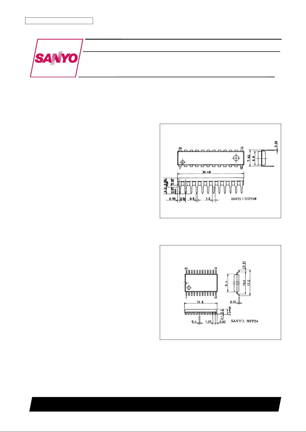
Package Dimensions
unit: mm
3092-DIP24W
unit: mm
3155-MFP24
CMOS IC
Ordering number : EN4624B
73696HA (OT)/N1094TH (OT)/82793JN No. 4624-1/14
SANYO: DIP24W
[LC78835K]
SANYO: MFP24
[LC78835KM]
SANYO Electric Co.,Ltd. Semiconductor Bussiness Headquarters
TOKYO OFFICE Tokyo Bldg., 1-10, 1 Chome, Ueno, Taito-ku, TOKYO, 110 JAPAN
18 Bits Digital Filter and D/A Converter
for Digital Audio
LC78835K, 78835KM
Specifications
Absolute Maximum Ratings at Ta = 25°C, VSS= 0°C
Allowable Operating Ranges
DC Characteristics
at Ta = –30 to +75°C, VDD= 3.5 to 5.5 V, VSS= 0 V
Note: * 3, 4, 5, 6, 7, 11, 13, 14, 15, 16, 17 and 18 pin
AC Characteristics
at Ta = –30 to +75°C, VDD= 3.5 to 5.5 V, VSS= 0 V
No. 4624-2/14
LC78835K, 78835KM
Parameter Symbol Conditions Ratings Unit
Maximum supply voltage V
DD
max –0.3 to + 7.0 V
Input voltage V
IN
–0.3 to VDD+ 0.3 V
Output voltage V
OUT
–0.3 to VDD+ 0.3 V
Operating temperature Topr –30 to + 75 °C
Storage temperature Tstg –40 to + 125 °C
Parameter Symbol Conditions
Ratings
Unit
min typ max
Supply voltage V
DD
3.5 5.0 5.5 V
Reference voltage high Vref H V
DD
– 0.3 V
DD
V
Reference voltage low Vref L 0 0.3 V
Operating temperature Topr –30 +75 °C
Parameter Symbol Conditions
Ratings
Unit
min typ max
Input high level voltage (1) V
IH
1 3, 4, 5, 6, 7, 13, 14, 15, 16, 17 and 18 pin 2.2 V
Input low level voltage (1) V
IL
1 3, 4, 5, 6, 7, 13, 14, 15, 16, 17 and 18 pin 0.8 V
Input high level voltage (2) V
IH
2 11 pin 0.7V
DD
V
Input low level voltage (2) V
IL
2 11 pin 0.3V
DD
V
Output high level voltage V
OH
9 pin: IOH= –3 mA 2.4 V
Output low level voltage V
OL
9 pin: IOL= 3 mA 0.4 V
Input leakage current I
L
*, VI= VSS, V
DD
–25 +25 µA
Parameter Symbol Conditions
Ratings
Unit
min typ max
Oscillation frequency f
X
XIN pin for crystal oscillator 1.0 25 MHz
Clock pulse width t
CW
With external clock input to other than XIN pin
18 ns
Clock pulse phase t
CY
With external clock input to other than XIN pin
40 1000 ns
BCLK pulse width t
BCW
60 ns
BCLK pulse phase t
BCY
120 ns
Data setup time t
DS
40 ns
Data hold time t
DH
40 ns
LRCK setup time t
LRS
40 ns
LRCK hold time t
LRH
40 ns

Audio Input Waveforms
Electrical Characteristics (1)
at Ta = 25°C, AVDD= DVDD= VrefH = 5.0 V, AGND = DGND = VrefL = 0 V, unless otherwise specified
Note: 1. “0 dB” signifies full scale.
2. XIN pulse width (pin 11) 1.5 to 3.5 V, fx = 16.9344 MHz
Test circuit: Based on application circuit
No. 4624-3/14
LC78835K, 78835KM
Parameter Symbol Conditions
Ratings
Unit
min typ max
D/A converter resolution RES 18 Bits
Total harmonic distortion THD At 1 kHz, 0 dB
*1
0.08 %
Dynamic range DR At 1 kHz, –60 dB 90 dB
Crosstalk CT At 1 kHz, 0 dB –85 dB
Signal-to-noise ratio S/N JIS-A 96 dB
Full-scale output voltage VFS 3.0 V
P-P
Power dissipation Pd
*2
135 200 mW
Output load resistance RL 21, 23 pin 5 kΩ
Electrical Characteristics (2)
at Ta = 25°C, AVDD= DVDD= VrefH 3.5 V, AGND = DGND = VrefH = 0 V, unless otherwise specified
Note: 1. “0 dB” signifies full scale.
2. XIN pulse width (pin 11) 1.0 to 2.5 V, fx = 16.9344 MHz
Test circuit: Based on application circuit
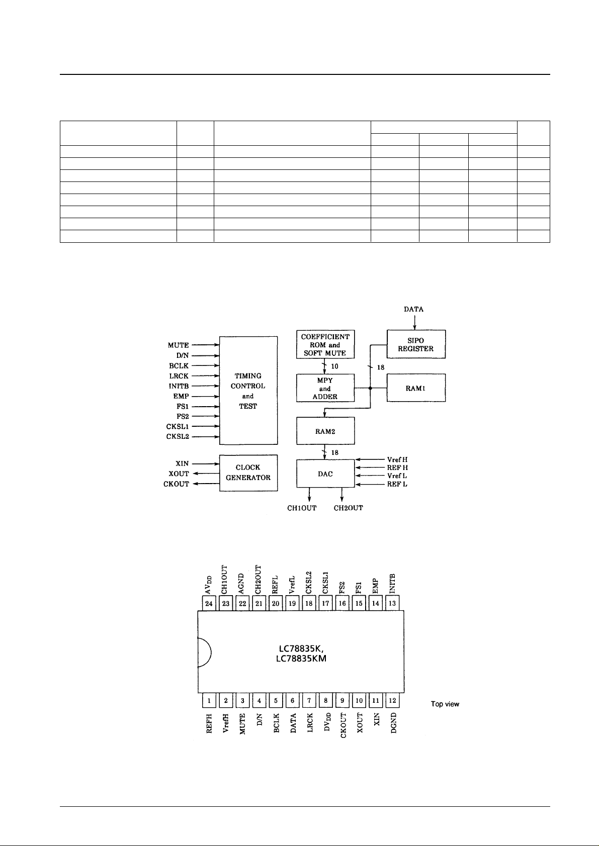
Block Diagram
Pin Assignment
No. 4624-4/14
LC78835K, 78835KM
Parameter Symbol Conditions
Ratings
Unit
min typ max
D/A converter resolution RES 18 Bits
Total harmonic distortion THD At 1 kHz, 0dB
*1
0.09 %
Dynamic range DR At 1 kHz, –60 dB 90 dB
Crosstalk CT At 1 kHz, 0 dB –85 dB
Signal-to-noise ratio S/N JIS-A 96 dB
Full-scale output voltage VFS 2.1 V
P-P
Power dissipation Pd
*2
50 75 mW
Output load resistance RL 21, 23 pin 15 kΩ
Pin Description
No. 4624-5/14
LC78835K, 78835KM
Number Name Description
1 REFH Reference voltage “H” pin
Normally connected to AGND via a capacitor
2 VrefH Reference voltage “H” input pin
3 MUTE Mute signal input pin
Soft mute is on when high
4 D/N Normal/double-speed operation toggle
Double-speed operation when high, normal operation when low
5 BCLK Bit clock input pin
6 DATA Digital audio data input pin
2’s complement code, with input from the most significant bit (MSB)
7 LRCK Left-right clock input pin
Channel 1 when high, channel 2 when low
8 DV
DD
Digital power supply pin
9 CKOUT Clock output pin
When at 392 fs: 196 fs clock
When not at 392 fs: XIN-frequency clock
10 XOUT Crystal oscillator output pin (system clock output pin)
11 XIN Crystal oscillator input pin (system clock input pin)
12 DGND Digital ground pin
13 INITB Initialization signal input pin
Initialization performed when low
14 EMP On/Off toggle for the de-emphasis filter
On when high, off when low
15 FS1 32 kHz/44.1 kHz/48 kHz selector for the de-emphasis filter
16 FS2
17 CKSL1 System clock selector pin
18 CKSL2
19 VrefL Reference voltage “L” input pin
20 REFL Reference voltage “L” pin
Normally connected to AGND via a capacitor
21 CH2OUT Channel 2 analog output pin
22 AGND Analog ground pin
23 CH1OUT Channel 1 analog output pin
24 AV
DD
Analog power supply pin
FS1 L H H L
FS2 L L H H
fs 44.1 kHz 32 kHz 48 kHz
CKSL1 CKSL2 System Clock
L L 384 fs
L H 392 fs
H L 448 fs
H H 512 fs

Description of Operation
1. Digital Filter
The LC78835K and 78835KM perform arithmetic functions as shown in the following block diagrams.
• Oversampling
Constructed of twice as many interpolation filters with a cascade connection arrangement using finite-impulseresponse (FIR) filters. When operating in normal-rate mode, data is transferred through a three-stage cascading
process consisting of 43rd-order, 11th-order, and third-order finite impulse response (FIR) filters connected
together to produce an eight-times oversampled signal. When operating in double-rate mode, data is transferred
through a two-stage cascading process consisting of 43rd-order and second-order finite-impulse-response (FIR)
connected filters to give a four-times oversampled signal. For further details concerning filter characteristics, refer
to page 12.
• De-emphasis
Digital de-emphasis is performed using a first-order infinite-impulse-response (IIR) filter. Filter supported
sampling frequencies include fs = 32 kHz, 44.1 kHz and 48 kHz (frequencies are all doubled with double-rate
mode).
No. 4624-6/14
LC78835K, 78835KM

For further details concerning filter characteristics when de-emphasis is on, refer to page 13.
— De-emphasis on/off
De-emphasis on: EMP pin = “H”
De-emphasis off: EMP pin = “L”
— Selection of filter coefficient
• Soft Mute
Soft muting is performed using the built-in digital attenuator. The attenuation amount of the attenuator circuit is as
follows:
20 log (ATT/256) dB
Although ATT = 0 to 256, when ATT = 0, attenuation sets to – ∞. If the MUTE pin is set to “H” level, ATT
approaches 0 in single-decreasing increments and the attenuation changes towards – ∞. On the other hand, when
the MUTE pin is set to the “L” level, ATT approaches 256 in single-increasing increments and the attenuation
amount changes to approach 0. The approximate speed during soft mute is 1024/fs.
• Noise Shaper
In order to reduce noise during DF arithmetic output requantization, the first-order noise shaper is utilized.
• Double-Rate Support
When the D/N pin is set to “H” level, CD high-speed playback is supported. At this time, BCLK, LRCK and
DATA are input at double the frequency of normal operating times. The system clock operates at 384 fs and with
a clock speed of 512 fs, double-rate is supported. Note that test mode is enabled for clock speeds of 392 fs and
448fs and double-rate is not supported.
Normal-rate mode: D/N pin = “L”
Double-rate mode: D/N pin = “H”
No. 4624-7/14
LC78835K, 78835KM
FS1 L H H L
FS2 L L H H
fs 44.1 kHz 32 kHz 48 kHz

2. Initialization
Initialization is necessary when power is applied or the system clock is replaced. When the INITB pin has been set
to an “L” level, the supply to XIN, BCLK, and LRCK should be connected only after the supply has stabilized at the
“L” level. As shown in the figure, a period greater than one LRCK cycle is required.
When INITB = “L,” all 18-bit digital filter outputs set to 0, and the D/A converter’s output (CH1OUT, CH2OUT)
equals 0 analog output (approximately (VREFH + VREFL)/2 electric potential).
3. System Clock
This IC supports four system clock speeds including 384 fs, 392 fs, 448 fs, and 512 fs. These may be selected using
the CKSL1 and CKSL2 pins.
• CKOUT Pin
When operating at 392 fs, clock output is 196 fs or half that of the system clock. All other speeds result in clock
output equal to that of the system.
No. 4624-8/14
LC78835K, 78835KM
CKSL1 CKSL2 System Clock
L L 384 fs
L H 392 fs
H L 448 fs
H H 512 fs

4. Digital Audio Data Input
Digital audio data supports MSB first and 2’s complement code using a 16-bit serial signal. 16-bit serial data is input
from the DATA pin at the edge of BCLK rising and is input to the internal register along with readings at the rising and
falling edges of LRCK.
Digital Audio Data Input Timing
No. 4624-9/14
LC78835K, 78835KM

5. Digital-to-Analog (D/A) Converter
These chips have built-in output operational amplifiers which use two independent on-chip D/A converters for CH1
and CH2. Both use dynamic level shift, combining resistance strings (R-string D/A conversion), pulse-width
modulation (PWM D/A conversion) and level shift D/A conversion modes. (See figure below.)
• Resistance String (R-string) D/A Converter
This 9-bit D/A converter circuit has 512 (=29) unit resistors (R) connected in series so that a potential applied to
both ends is subjected to 512-way division. The two adjoining potentials V2 and V1 of the divided potentials
corresponding to the values of the 9 MSBs of data (D15 to D9) are sent via a switching circuit to the PWM D/A
converter. At this point, V2 – V1 = (VH – VL)/512.
No. 4624-10/14
LC78835K, 78835KM

• Pulse-Width Modulation (PWM) D/A Converter
This is a 3-bit circuit that applies pulse width modulation to voltages V2 and V1 output from the R-string D/A
converter to produce an 8-way division. Depending on the value of the data in bits D8 to D6, one of the voltages,
V2 or V1, is output to the CH1OUT (or CH2OUT) pin.
• Level Shift D/A Converter
The variable resistors VRH and VRL are connected in series to the two ends of the R-string D/A converter
resistance, configuring a 6-bit D/A conversion circuit. Depending on the values of the data in the LSBs (bits D5 to
D0), VRH and VRL change as follows.
(1) The sum of VRH and VRL is constant, irrespective of the data value.
(2) Irrespective of the data value, VRH and VRL are in the range of 0 to 63R/512 (where R is the unit resistance of
the R-string D/A converter) and resistance changes in R/512 steps in accordance with the data value.
This means that the R-string D/A converter outputs, V2 and V1, each vary in the range of 0 to 63 × ∆V/512 (∆V =
(VH - VL)/512) in ∆V/512 steps.
— Vref H/L, REF H/L Pins
The voltage on the Vref pins, used to apply the reference voltage to the resistance strings, are usually set so that
VrefH = AVDDand VrefL = AGND. In addition, a 10 µF rated condenser connects REFH and AGND as well
as REFL and AGND. When VrefH = 5.0 V, VrefL = 0 V, the LC78835K on-chip RH and RL resistors
maximum output amplitude at 0 dB playback is output in the 3.0 Vp-p range extending from a minimum 0.6 V
to maximum 3.6 V.
No. 4624-11/14
LC78835K, 78835KM

Filter Characteristics (theoretical values)
Normal-rate mode: 8 fs oversampling
Double-rate mode: 4 fs oversampling
Ripple: within ±0.05 dB
Attenuation amount: –40 dB or less
•Normal Rate (De-emphasis Off)
No. 4624-12/14
LC78835K, 78835KM
•Double Rate (De-emphasis Off)
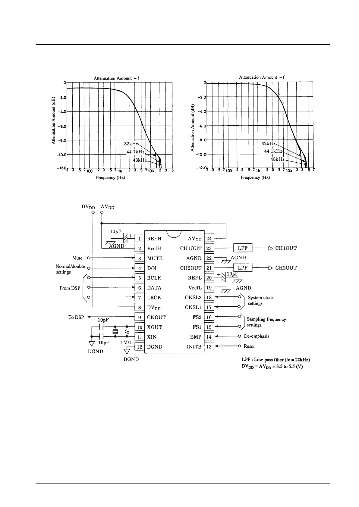
Pass Band Characteristics with De-emphasis On
• Normal Rate • Double Rate
Sample Application Circuit
Note: 1. Within the sample application circuit, DVDDconnects to DGND as the digital ground, and AVDDconnects to
AGND as the analog ground.
2. For AVDDand VrefH, a low-impedance high-stability power supply (commercially available 3-pin regulator or
compatible) should be used.
3. If 8-pin (DVDD) and 24-pin (AVDD) rise timings deviate, latch-up may occur. For this reason, no difference
should exist between 8 and 24 pin power application timing.
4.A clock signal must be supplied to the XIN pin immediately after power is applied. The IC may be destroyed if
the XIN pin is held either high or low when power is applied.
No. 4624-13/14
LC78835K, 78835KM

No. 4624-14/14
LC78835K, 78835KM
This catalog provides information as of July, 1996. Specifications and information herein are subject to change
without notice.
■ No products described or contained herein are intended for use in surgical implants, life-support systems, aerospace
equipment, nuclear power control systems, vehicles, disaster/crime-prevention equipment and the like, the failure of
which may directly or indirectly cause injury, death or property loss.
■ Anyone purchasing any products described or contained herein for an above-mentioned use shall:
① Accept full responsibility and indemnify and defend SANYO ELECTRIC CO., LTD., its affiliates, subsidiaries and
distributors and all their officers and employees, jointly and severally, against any and all claims and litigation and all
damages, cost and expenses associated with such use:
➁ Not impose any responsibility for any fault or negligence which may be cited in any such claim or litigation on
SANYO ELECTRIC CO., LTD., its affiliates, subsidiaries and distributors or any of their officers and employees
jointly or severally.
■ Information (including circuit diagrams and circuit parameters) herein is for example only; it is not guaranteed for
volume production. SANYO believes information herein is accurate and reliable, but no guarantees are made or implied
regarding its use or any infringements of intellectual property rights or other rights of third parties.
 Loading...