

Ordering number : EN*5212
D3095HA (OT) No. 5212-1/11
Overview
The LC78833M and LC78833V are CMOS 16-bit D/A
converters with built-in 4× oversampling digital filters.
Functions and Features
[Digital Filter Block]
•4×oversampling filters: Two FIR filter stages (33rd and
ninth order)
• De-emphasis filter: Supports a 44.1 kHz sampling
frequency (fs).
[D/A Converter Block]
• Dynamic level shifting conversion 16-bit D/A converter
• D/A converters for two channels (synchronized outputs)
on a single chip
• On-chip output operational amplifiers
• System clock: 384fs
• 5-V single-voltage power supply
• Supports low-voltage operation (3.0 V)
• Implemented in a Si gate CMOS process for low power.
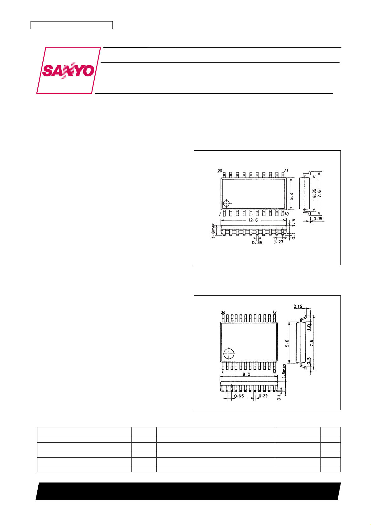
Package Dimensions
unit: mm
3036B-MFP20
unit: mm
3175A-SSOP24
Preliminary
SANYO: MFP20
[LC78833M]
SANYO: SSOP24
[LC78833V]
LC78833M, 78833V
SANYO Electric Co.,Ltd. Semiconductor Bussiness Headquarters
TOKYO OFFICE Tokyo Bldg., 1-10, 1 Chome, Ueno, Taito-ku, TOKYO, 110-8534 JAPAN
Digital Audio 16-Bit D/A Converter
with Built-In Digital Filters
CMOS LSI
Specifications
Absolute Maximum Ratings at Ta = 25°C, VSS= 0 V
Parameter Symbol Conditions Ratings Unit
Maximum supply voltage V
DD
max –0.3 to +7.0 V
Maximum input voltage V
IN
max –0.3 to VDD+ 0.3 V
Maximum output voltage V
OUT
max –0.3 to VDD+ 0.3 V
Operating temperature Topr –30 to +75 °C
Storage temperature Tstg –40 to +125 °C
Allowable Operating Ranges
Electrical Characteristics (1)
at Ta = 25°C, AVDD= DVDD= Vref H = 5.0 V, AGND = DGND = Vref L = 0 V, unless otherwise specified
Note: 1.Here, 0 dB means full scale.
2. Pin numbers in parentheses are for the LC78833V.
Electrical Characteristics (2)
at Ta = 25°C, AVDD= DVDD= Vref H = 3.0 V, AGND = DGND = Vref H = 0 V, unless otherwise specified
Note: 1.Here, 0 dB means full scale.
2. Pin numbers in parentheses are for the LC78833V.
No. 5212-2/11
LC78833M, 78833V
Parameter Symbol Conditions min typ max Unit
Supply voltage V
DD
3.0 5.0 5.5 V
Reference voltage (high) Vref H V
DD
– 0.3 V
DD
V
Reference voltage (low) Vref L 0 +0.3 V
Parameter Symbol Conditions min typ max Unit
D/A converter resolution RES 16 Bit
Total harmonic distortion THD At 1 kHz and 0 dB
*1
0.08 %
Dynamic range DR At 1 kHz, –60 dB 92 94 dB
Crosstalk CT At 1 kHz and 0 dB –85 dB
Signal-to-noise ratio S/N JIS-A 96 100 dB
Full-scale output voltage VFS 2.6 2.8 3.0 Vp-p
Power dissipation Pd At fs = 44.1 kHz 60 90 mW
Output load resistance RL Pins 1 and 20 (1 and 24)
*2
5 kΩ
Parameter Symbol Conditions min typ max Unit
D/A converter resolution RES 16 Bit
Total harmonic distortion THD At 1 kHz and 0 dB
*1
0.10 %
Dynamic range DR At 1 kHz, –60 dB 90 92 dB
Crosstalk CT At 1 kHz and 0 dB –85 dB
Signal-to-noise ratio S/N JIS-A 94 98 dB
Full-scale output voltage VFS 1.55 1.7 1.85 Vp-p
Power dissipation Pd At fs = 44.1 kHz 15 25 mW
Output load resistance RL Pins 1 and 20 (1 and 24)
*2
30 kΩ

Block Diagram
DC characteristics at Ta = –30 to 75°C, VDD= 3.0 to 5.5 V, VSS= 0 V
Note: * Pins in parentheses apply to the LC78833V.
AC Characteristics at Ta = –30 to 75°C, VDD= 3.0 to 5.5 V, VSS= 0 V
No. 5212-3/11
LC78833M, 78833V
Parameter Symbol Conditions min typ max Unit
Input high-level voltage (1) V
IH
1 Pins 5, 6, 7, 12, 13, and 14 (pins 6, 7, 8, 14, 16, and 17)* 2.2 V
Input low-level voltage (1) V
IL
1 Pins 5, 6, 7, 12, 13, and 14 (pins 6, 7, 8, 14, 16, and 17)* 0.8 V
Input high-level voltage (2) V
IH
2 Pin 8 (pin 9)* 0.7 V
DD
V
Input low-level voltage (2) V
IL
2 Pin 8 (pin 9)* 0.3 V
DD
V
Output high-level voltage V
OH
Pin 9 (pin 11)*: IOH= –3 mA 2.4 V
Output low-level voltage V
OL
Pin 9 (pin 11)*: IOL= 3 mA 0.4 V
Input leakage current I
L
Pins 5, 6, 7, 8, 12, 13, and 14
–25 +25 µA
(pins 6, 7, 8, 9, 14, 16, and 17)*: V
I
= VSS, V
DD
Parameter Symbol Conditions min typ max Unit
Clock pulse width t
CW
25 ns
Clock pulse period t
CY
50 1000 ns
BCLK pulse width t
BCW
60 ns
BCLK pulse period t
BCY
120 ns
Data setup time t
DS
40 ns
Data hold time t
DH
40 ns
LRCK setup time t
LRS
40 ns
LRCK hold time t
LRH
40 ns
BCLK rise time t
Br
40 ns
BCLK fall time t
Bf
40 ns
SYSCLK rise time t
Sr
20 ns
SYSCLK fall time t
Sf
20 ns
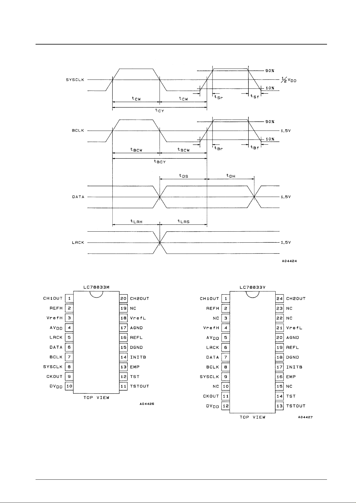
Audio Input Waveforms
Pin Assignments
No. 5212-4/11
LC78833M, 78833V

Pin Functions
No. 5212-5/11
LC78833M, 78833V
Pin No.
Pin Description
LC78833M LC78833V
1 1 CH1OUT Channel 1 analog output
2 2 REFH
High-level reference voltage
Normally connected to AGND through a capacitor.
— 3 NC No connection
3 4 Vref H High-level reference voltage input
4 5 AV
DD
Analog system power supply
5 6 LRCK
LR clock input
A high level specifies channel 1 and a low level channel 2.
6 7 DATA
Digital audio data input
Accepts data in a two’s complement MSB first format.
7 8 BCLK Bit clock input
8 9 SYSCLK System clock input (384fs)
— 10 NC No connection
9 11 CKOUT System clock output (384fs)
10 12 DV
DD
Digital system power supply
11 13 TSTOUT Test output
12 14 TST
Test output
This pin must be connected to DGND in normal operation.
— 15 NC No connection
De-emphasis filter on/off control input
13 16 EMP A high level specifies on and a low level off.
This function supports a sampling frequency fs of 44.1 kHz.
14 17 INITB Initialization input. A low level input to this pin initializes the IC.
15 18 DGND Digital system ground
16 19 REFL
Low-level reference voltage
Normally connected to AGND through a capacitor.
17 20 AGND Analog system power supply
18 21 Vref L Low-level reference voltage input
— 22 NC No connection
19 23 NC No connection
20 24 CH2OUT Channel 2 analog output

LC78833M/V Operation
1. Digital Filters
The LC78833M and LC78833V perform the computations shown in the figure.
• Oversampling
The oversampling circuit in these ICs consists of two 2× interpolation filters (implemented as FIR filters)
connected vertically.
In particular, these ICs implement 4× oversampling by the vertical connection of two FIR filter stages, a 33rd-order
stage and a ninth-order stage. See page 9 for the filter characteristics.
• De-emphasis
A first-order IIR filter is used for de-emphasis. The filter coefficients are optimized for a sampling frequency of
44.1 kHz. See page 9 for the filter characteristics when de-emphasis is applied.
— De-emphasis on/off switching
De-emphasis is on when the EMP pin is high.
De-emphasis is off when the EMP pin is low.
2. Digital Audio Data Input
These ICs handle digital audio data in a 16-bit two’s complement MSB first format. The 16-bit serial data is input to
an internal register from the DATA pin on BCLK rising edges and read in on rising and falling edges of the LRCK
signal.
No. 5212-6/11
LC78833M, 78833V

3. Initialization
These ICs must be initialized when power is first applied and when the system clock frequency is changed.
Initialization is performed by applying a low level to the INITB pin. That low level must be held for at least one full
cycle of the LRCK signal after the power supply voltage has stabilized and the SYSCLK, BCLK, and LRCK signals
have been applied.
When INITB is low, all 16 bits of the digital filter outputs go to 0, and the D/A converter outputs (CH1OUT and
CH2OUT) go to the analog 0 level, which is a potential equal to (REFH +REFL)/2.
4. System Clock
These ICs support a 384fs system clock. Apply a 384fs clock to the SYSCLK pin.
• CKOUT pin
The SYSCLK and CKOUT pins are related as shown in the figure below.
No. 5212-7/11
LC78833M, 78833V

5. D/A Converter Block
Channel 1 and channel 2 each include an independent 16-bit D/A converter and an output operational amplifier.
These D/A converters use the dynamic level-shifting conversion scheme shown in the figure below. This scheme
combines three conversion techniques, resistor string D/A conversion, PWM (pulse width modulation) D/A
conversion, and level-shifting D/A conversion.
No. 5212-8/11
LC78833M, 78833V

• Resistor string D/A converter
This 8-bit D/A converter uses a total of 256 (= 28) unit-resistance (R) resistors connected in series to voltage divide
the potential applied to the ends of that resistor string into 256 equal intervals. Of these resistor-divided potentials,
two adjacent potentials, V1 and V2, are selected by a switching circuit according to the value of the upper 8 bits
(D15 to D8) of the data. These two potentials are output to the PWM D/A converter. Note that these potentials are
related as follows:
V2 – V1 = (VH – VL)/256
• PWM D/A converter
This 4-bit D/A converter divides (by 16) the interval between the two potentials, V1 and V2, output by the resistorstring D/A converter. This circuit outputs one or the other of the V1 and V2 potentials from the CH1OUT (or
CH2OUT) pin according to the value of the middle 4 bits (D7 to D4) of the data.
• Level shifting D/A converter
This 4-bit D/A converter is implemented by connecting the variable resistors VRH and VRL in series at the ends of
the resistor-string D/A converter. The values of the VRH and VRL variable resistors are modified according to the
value of the low-order 4 bits of the data as follows:
— The value of VRH + VRL is held fixed regardless of the value of the data.
— The values of VRH and VRL are changed in R/256 unit steps (where R is the value of the resistor-string D/A
converter unit resistors) over the range zero to 15·R/256.
This causes the resistor-string D/A converter V1 and V2 outputs to change in ∆V/256 steps (where ∆V = (VH –
VL)/256) over the range 0 to 15 × ∆V/256 according to the value of the lower 4 bits of the data.
— The Vref H/L and REFH/L pins
The Vref H/L pins provide the reference voltage to the resistor string, and are normally connected to AVDDand
AGND, respectively. REFH and REFL are each connected to AGND through a capacitor of about 10 µF.
The maximum output amplitude is acquired when Vref H is 5.0 V and Vref L is 0 V. The internal resistors RH
and RL cause the output range to be between 0.7 V (minimum) and 3.5 V (maximum) (2.8 Vp-p) for 0 dB.
Filter Characteristics (as calculated)
4× oversampling
Ripple: Less than ±0.1 dB
Attenuation: –35 dB or lower
No. 5212-9/11
LC78833M, 78833V

Application Circuit Example
Note 1. VDDand Vref H must be provided from a low-impedance, high-stability power supply, for example, a
commercial three-terminal regulator or equivalent.
2. Since it is possible for the IC to latch up if there is a discrepancy between the pin 4 (AVDD) and pin 10 (DVDD)
power supply power-on timing, application circuits should be designed so that there is no time difference
between the application of these voltages.
3. Bypass capacitors of at least 47 µF must be inserted between AVDDand AGND and between DVDDand
DGND. These capacitor must be placed as close as possible to the IC.
4. Bypass capacitors of at least 10 µF must be inserted between REFH and AGND and between REFL and
AGND for reference voltage stability.
No. 5212-10/11
LC78833M, 78833V

No. 5212-11/11
LC78833M, 78833V
Power On Timing
1. The analog power supply (AVDD) and the digital power supply (DVDD) should be applied (or removed) at the same
time.
2. If a time difference between application of the analog and digital power supplies cannot be avoided, the timing must
meet the following conditions:
• The power supply power up (and power down) time differences must be under 3 ms. (See Figure 1.)
• If the time difference exceeds 3 ms, the rise (fall) time of the power supply that rises (falls) first must be at least
5 ms, and the time difference must be under 50 ms. (See Figure 2.)
Figure 1
Figure 2
This catalog provides information as of February, 1997. Specifications and information herein are subject to
change without notice.
■ No products described or contained herein are intended for use in surgical implants, life-support systems, aerospace
equipment, nuclear power control systems, vehicles, disaster/crime-prevention equipment and the like, the failure of
which may directly or indirectly cause injury, death or property loss.
■ Anyone purchasing any products described or contained herein for an above-mentioned use shall:
➀ Accept full responsibility and indemnify and defend SANYO ELECTRIC CO., LTD., its affiliates, subsidiaries and
distributors and all their officers and employees, jointly and severally, against any and all claims and litigation and all
damages, cost and expenses associated with such use:
➁ Not impose any responsibility for any fault or negligence which may be cited in any such claim or litigation on
SANYO ELECTRIC CO., LTD., its affiliates, subsidiaries and distributors or any of their officers and employees
jointly or severally.
■ Information (including circuit diagrams and circuit parameters) herein is for example only; it is not guaranteed for
volume production. SANYO believes information herein is accurate and reliable, but no guarantees are made or implied
regarding its use or any infringements of intellectual property rights or other rights of third parties.
 Loading...