

Page 1

CMOS LSI
Ordering number : EN*5107A
D3098HA (OT)/62295TH (OT) No. 5107-1/6
Preliminary
SANYO Electric Co.,Ltd. Semiconductor Bussiness Headquarters
TOKYO OFFICE Tokyo Bldg., 1-10, 1 Chome, Ueno, Taito-ku, TOKYO, 110-8534 JAPAN
16-Bit D/A Converter for Digital Audio
LC78817, 78817M
Overview
The LC78817 and LC78817M are 16-bit CMOS D/A
converters for use in digital audio systems. They adopt a
dynamic level shifting conversion technique that uses a
resistor string for the upper 8 bits, PWM for the middle 4
bits, and level shifting for the lower 4 bits.
Package Dimensions
unit: mm
3001B-DIP8
Features
• Support for twos complement data
• Two D/A converter channels on a single chip
(synchronous outputs)
• Maximum conversion frequency: 192 kHz (supports 4×
oversampling)
• On-chip output operational amplifiers
• No deglitching circuit required
• Si-gate CMOS process for low power dissipation
• Single 5 V power supply
• Low voltage operation (3.0 V) possible
unit: mm
3086A-MFP10S
1
10
5
6
0.55
1.8max
1.00.35
5.1
0.15
6.4
1.5
0.1
4.4
5.15 0.625
SANYO: MFP10S
[LC78817M]
Specifications
Absolute Maximum Ratings at Ta = 25°C
Parameter Symbol Conditions Ratings Unit
Maximum supply voltage V
DD
max –0.3 to +7.0 V
Input voltage V
IN
–0.3 to VDD+ 0.3 V
Output voltage V
OUT
–0.3 to VDD+ 0.3 V
Operating temperature Topr –30 to +75 °C
Storage temperature Tstg –40 to +125 °C
[LC78817]
SANYO: DIP8
Any and all SANYO products described or contained herein do not have specifications that can handle
applications that require extremely high levels of reliability, such as life-support systems, aircraft’s
control systems, or other applications whose failure can be reasonably expected to result in serious
physical and/or material damage. Consult with your SANYO representative nearest you before using
any SANYO products described or contained herein in such applications.
SANYO assumes no responsibility for equipment failures that result from using products at values that
exceed, even momentarily, rated values (such as maximum ratings, operating condition ranges, or other
parameters) listed in products specifications of any and all SANYO products described or contained
herein.
0.5
9.4
1.4
5
6.4
7.62
0.25
4
3.0
3.9max
3.2
0.51min
8
1
0.89 2.54
Page 2
Allowable Operating Ranges
DC Characteristics at Ta = –30 to +75°C, V
DD
= 3.0 to 5.5 V, VSS= 0 V
AC Characteristics at Ta = –30 to +75°C, V
DD
= 3.0 to 5.5 V, VSS= 0 V
Electrical Characteristics (1) at Ta = 25°C, V
DD
= 5.0 V, GND = 0 V
Note: * Values in parentheses apply to the LC78817M
Test circuit: Use a circuit that conforms to the sample application circuit shown and a 176.4 kHz sampling frequency (Fs).
No. 5107-2/6
LC78817, 78817M
Parameter Symbol Conditions min typ max Unit
Supply voltage V
DD
3.0 5.0 5.5 V
Operating temperature Topr –30 +75 °C
Parameter Symbol Conditions min typ max Unit
Input high level voltage V
IH
2.2 V
Input low level voltage V
IL
0.8 V
Parameter Symbol Conditions min typ max Unit
Clock pulse width T
BCW
BCLK 35 ns
Setup time T
DS
LRCK, DATA 20 ns
Hold time T
DH
LRCK, DATA 20 ns
Rise time Tr BCLK, LRCK 30 ns
Fall time Tf BCLK, LRCK 30 ns
Parameter Symbol Conditions min typ max Unit
Resolution RES 16 bits
Conversion frequency F
S
192 kHz
Total harmonic distortion THD1 f = 1 kHz, 0 dB 0.09 %
Dynamic range D
R
f = 1 kHz, –60 dB 94 96 dB
Crosstalk C·T f = 1 kHz, 0 dB –85 dB
Signal-to-noise ratio S/N JIS-A 96 100 dB
Full-scale output voltage VFS 2.8 3.0 3.2 Vp-p
Power dissipation Pd 30 45 mW
Output load resistance R
L
* Pins 1 and 8 (1 and 10) 5 kΩ
Page 3

Electrical Characteristics (2) at Ta = 25°C, VDD= 3.0 V, GND = 0 V
Note: * Values in parentheses apply to the LC78817M
Test circuit: Use a circuit that conforms to the sample application circuit shown and a 176.4 kHz sampling frequency (Fs).
Pin Assignments
Block Diagram
No. 5107-3/6
LC78817, 78817M
Parameter Symbol Conditions min typ max Unit
Resolution RES 16 bits
Conversion frequency F
S
192 kHz
Total harmonic distortion THD1 f = 1 kHz, 0 dB 0.1 %
Dynamic range D
R
f = 1 kHz, –60 dB 92 94 dB
Crosstalk C·T f = 1 kHz, 0 dB –85 dB
Signal-to-noise ratio S/N JIS-A 94 98 dB
Full-scale output voltage V
FS
1.65 1.8 1.95 Vp-p
Power dissipation Pd 5 7.5 mW
Output load resistance R
L
* Pins 1 and 8 (1 and 10) 30 kΩ
Top view
Page 4

Pin Functions
Operating Description
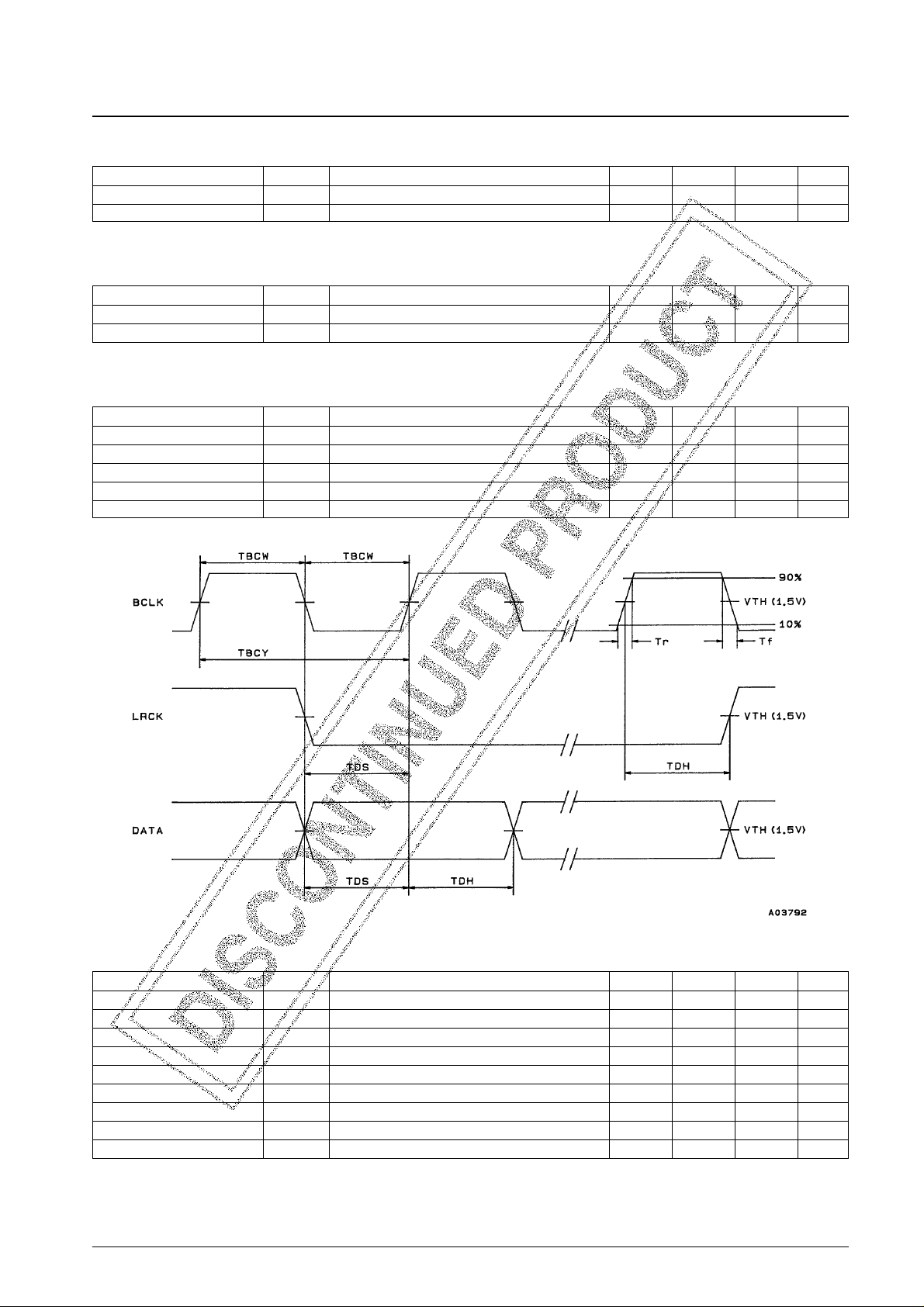
1. Digital Audio Data Input
The digital audio data is a 16-bit signal in an msb-first twos complement format. The 16 bits of data are acquired in
synchronization with the rising edge of BCLK starting with the msb. See the timing chart for details.
2. Conversion (see Figure 1)
The LC78817 and LC78817M includes two independent D/A converter circuits, one each for channels one and two.
It adopts a dynamic level shifting conversion technique that uses a resistor-string D/A converter, a PWM (pulse
width modulation) D/A converter, and a level shifting D/A converter. After latching the 16 bits of digital audio data
(D15 to D0):
the upper 8 bits (D15 to D8) are input to the resistor-string D/A converter, and
the middle 4 bits (D7 to D4) are input to the PWM D/A converter, and
the lower 4 bits (D8 to D0) are input to the level-shifting D/A converter.
• Resistor-string D/A converter
This is a D/A converter in which a total of 256 (= 2
8
) unit-resistance resistors are connected in series and the
potential applied to the ends of that resistor string is voltage divided into 256 equal intervals. Of these resistordivided potentials, two adjacent potentials, V1 and V2, are selected by a switching circuit according to the value of
the upper 8 bits of the data. These two potentials are output to the PWM D/A converter. Note that these potentials
are related as follows:
V2 – V1 = (VH – VL)/256
• PWM D/A converter
This is a 4-bit D/A converter that divides (by 16) the interval between the two potentials, V1 and V2, output by the
resistor-string D/A converter. This circuit outputs one or the other of the V1 and V2 potentials from the CH1OUT
(or CH2OUT) pin according to the value of the middle 4 bits of the data.
• Level shifting D/A converter
This 4-bit D/A converter is implemented by connecting the variable resistors VRH and VRL in series at the ends of
the resistor-string D/A converter. The values of the VRH and VRL variable resistors are modified according to the
value of the low-order 4 bits of the data as follows:
— The value of VRH + VRL is held fixed regardless of the value of the data.
— The values of VRH and VRL are changed in R/256 unit steps (where R is the value of the resistor-string D/A
converter unit resistors) over the range zero to 15R/256.
This causes the resistor-string D/A converter V1 and V2 outputs to change in ∆V/256 steps (where ∆V = (VH –
VL)/256) over the range 0 to 15 ×∆V/256 according to the value of the lower 4 bits of the data.
No. 5107-4/6
LC78817, 78817M
Pin No.
Symbol Function and Operation
LC78817 LC78817M
1 1 CH1OUT CH1 analog output (left channel)
22 V
DD
Power supply voltage
— 3 NC No connection
3 4 BCLK
Bit clock input
This pin inputs the clock used for bit serial input of the digital audio input data.
4 5 LRCK
L/R clock input
This pin inputs the signal that discriminates the left and right digital audio data signals.
5 6 DATA
Digital audio data input
This pin inputs data in an msb-first bit-serial format. (A twos complement representation is used.)
6 7 GND Ground
— 8 NC No connection
7 9 REFH
Reference voltage
Connect to ground through a capacitor.
8 10 CH2OUT CH2 analog output (right channel)
Page 5

LC78817 and LC78817M D/A Conversion Technique
Figure 1
Digital Audio Data Input (timing chart)
The digital audio data is a 16-bit serial signal in an msb-first twos complement format. The 16-bit serial data is input
from the DATA pin to an internal register on the rising edge of BCLK, and is acquired on the LRCK rising or falling
edge.
Note: BCLK must be a multiple of 16 times the LRCK period, i.e., 32, 48, or 64 clocks. Conversion errors in the PWM D/A converter (middle 4 bits of data)
will occur for any other number of clock cycles.
No. 5107-5/6
LC78817, 78817M
Page 6

PS No. 5107-6/6
LC78817, LC78817M
Sample Application Circuit
Note: A bypass capacitor must be connected between VDDand GND as close as possible to the LSI itself.
This catalog provides information as of December, 1998. Specifications and information herein are
subject to change without notice.
Specifications of any and all SANYO products described or contained herein stipulate the performance,
characteristics, and functions of the described products in the independent state, and are not guarantees
of the performance, characteristics, and functions of the described products as mounted in the customer’s
products or equipment. To verify symptoms and states that cannot be evaluated in an independent device,
the customer should always evaluate and test devices mounted in the customer’s products or equipment.
SANYO Electric Co., Ltd. strives to supply high-quality high-reliability products. However, any and all
semiconductor products fail with some probability. It is possible that these probabilistic failures could
give rise to accidents or events that could endanger human lives, that could give rise to smoke or fire,
or that could cause damage to other property. When designing equipment, adopt safety measures so
that these kinds of accidents or events cannot occur. Such measures include but are not limited to protective
circuits and error prevention circuits for safe design, redundant design, and structural design.
In the event that any or all SANYO products (including technical data, services) described or contained
herein are controlled under any of applicable local export control laws and regulations, such products must
not be exported without obtaining the export license from the authorities concerned in accordance with the
above law.
No part of this publication may be reproduced or transmitted in any form or by any means, electronic or
mechanical, including photocopying and recording, or any information storage or retrieval system,
or otherwise, without the prior written permission of SANYO Electric Co., Ltd.
Any and all information described or contained herein are subject to change without notice due to
product/technology improvement, etc. When designing equipment, refer to the “Delivery Specification”
for the SANYO product that you intend to use.
Information (including circuit diagrams and circuit parameters) herein is for example only; it is not
guaranteed for volume production. SANYO believes information herein is accurate and reliable, but
no guarantees are made or implied regarding its use or any infringements of intellectual property rights
or other rights of third parties.
 Loading...