

Overview
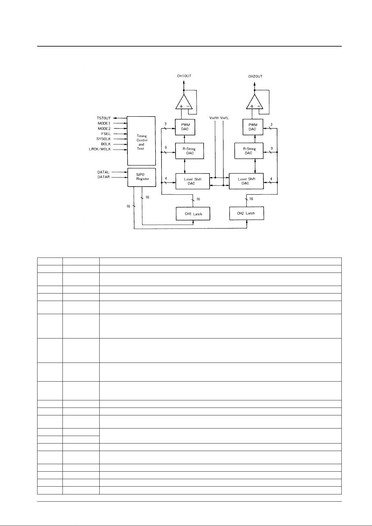
The LC78816MB and 78816MC are 16-bit CMOS D/A
converters for use in digital audio products. They employ
a dynamic level shift conversion technique that combines
a resistor string (for the upper 9 bits), PWM (for the
middle 3 bits), and level shifting (for the lower 4 bits).
Features
• Two’s complement data format
• Two D/A converter channels built in (in-phase outputs)
• Maximum conversion frequency of 400 kHz (support for
8 times oversampling)
• Built-in output op amps
• No deglitching circuit required
• Si gate CMOS process (low power consumption)
• 5 V single-voltage power supply
• Low voltage (3.5 V) operation possible
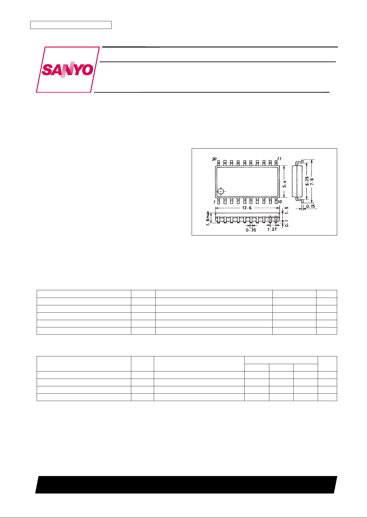
Package Dimensions
unit: mm
3036B-MFP20
CMOS LSI
63096HA (OT)/D1694TH(OT)/61893JN No. 4250-1/11
Preliminaly
SANYO: DIP20
[LC78816MB, 78816MC]
SANYO Electric Co.,Ltd. Semiconductor Bussiness Headquarters
TOKYO OFFICE Tokyo Bldg., 1-10, 1 Chome, Ueno, Taito-ku, TOKYO, 110 JAPAN
16-Bit D/A Converter for Use in
Digital Audio Products
LC78816MB, 78816MC
Ordering number : EN*4250C
Parameter Symbol Conditions Ratings Unit
Maximum power supply voltage V
DD
max –0.3 to +7.0 V
Input voltage V
IN
–0.3 to VDD+ 0.3 V
Output voltage V
OUT
–0.3 to VDD+ 0.3 V
Operating temperature Topr –30 to +75 °C
Storage temperature Tstg –40 to +125 °C
Specifications
Absolute Maximum Ratings at Ta = 25°C
Parameter Symbol Conditions
Ratings
Unit
min typ max
Power supply voltage V
DD
3.5 5.0 5.5 V
Reference voltage high V
refH
VDD– 0.3 V
DD
V
Reference voltage low V
refL
0 0.3 V
Operating temperature Topr –30 +75 °C
Allowable Operating Ranges
No. 4250-2/11
LC78816MB, 78816MC
Parameter Symbol Conditions
Ratings
Unit
min typ max
Input high level voltage (1) V
IH
Input pins other than SYSCLK 2.2 V
Input low level voltage (1) V
IL
Input pins other than SYSCLK 0.8 V
Input high level voltage (2) V
IH
The SYSCLK pin 0.7 V
DD
V
Input low level voltage (2) V
IL
The SYSCLK pin 0.3 V
DD
V
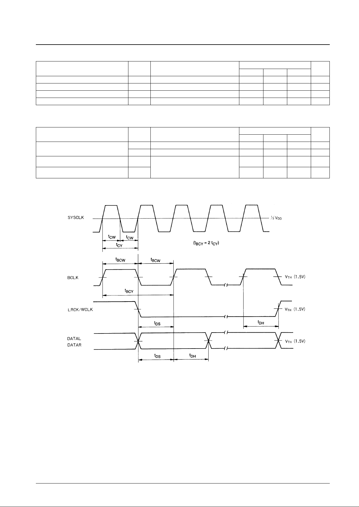
DC Characteristics at Ta = –30 to +75°C, VDD= 3.5 to 5.5 V, VSS= 0 V
Parameter Symbol Conditions
Ratings
Unit
min typ max
Clock pulse width
t
CW
SYSCLK 25 ns
t
BCW
BCLK 35 ns
Setup time t
DS
LRCK/WCLK
20 ns
Hold time t
DH
DATAL
20 ns
DATAR
AC Characteristics at Ta = –30 to +75°C, VDD= 3.5 to 5.5 V, VSS= 0 V
No. 4250-3/11
LC78816MB, 78816MC
Parameter Symbol Conditions
Ratings
Unit
min typ max
Resolution RES 16 Bits
Conversion frequency fs 400 kHz
Total harmonic distortion THD1 LC78816MB at 1 kHz, 0 dB 0.05* %
Total harmonic distortion THD1 LC78816MC at 1 kHz, 0 dB 0.08 %
Dynamic range D
R
At 1 kHz, –60 dB 94 96 dB
Cross talk C · T At 1 kHz, 0 dB –85 dB
Signal to noise ratio S/N JIS-A 96 dB
Full scale output voltage VFS 3.0 3.3 3.5 Vp-p
Power dissipation Pd 35 60 mW
Output load resistance R
L
Pins 1 and 20 5 kΩ
Electrical Characteristics (1) at Ta = 25°C, DVDD= AVDD= V
refH
= 5.0 V, DGND = AGND = V
refL
= 0.0 V
Notes:*: Screened units
Test circuit: based on the sample application circuit, with a sampling frequency (fs) of 88.2 kHz.
Parameter Symbol Conditions
Ratings
Unit
min typ max
Resolution RES 16 Bits
Conversion frequency fs 400 kHz
Total harmonic distortion THD1 LC78816MB at 1 kHz, 0 dB 0.06* %
Total harmonic distortion THD1 LC78816MC at 1 kHz, 0 dB 0.09 %
Dynamic range D
R
At 1 kHz, –60 dB 92 94 dB
Cross talk C · T At 1 kHz, 0 dB –85 dB
Signal to noise ratio S/N JIS-A 96 dB
Full scale output voltage VFS 2.0 2.3 2.5 Vp-p
Power dissipation Pd 10 20 mW
Output load resistance R
L
Pins 1 and 20 15 kΩ
Electrical Characteristics (2) at Ta = 25°C, DVDD= AVDD= V
refH
= 5.0 V, DGND = AGND = V
refL
= 0.0 V
Notes:*: Screened units
Test circuit: based on the sample application circuit, with a sampling frequency (fs) of 88.2 kHz.
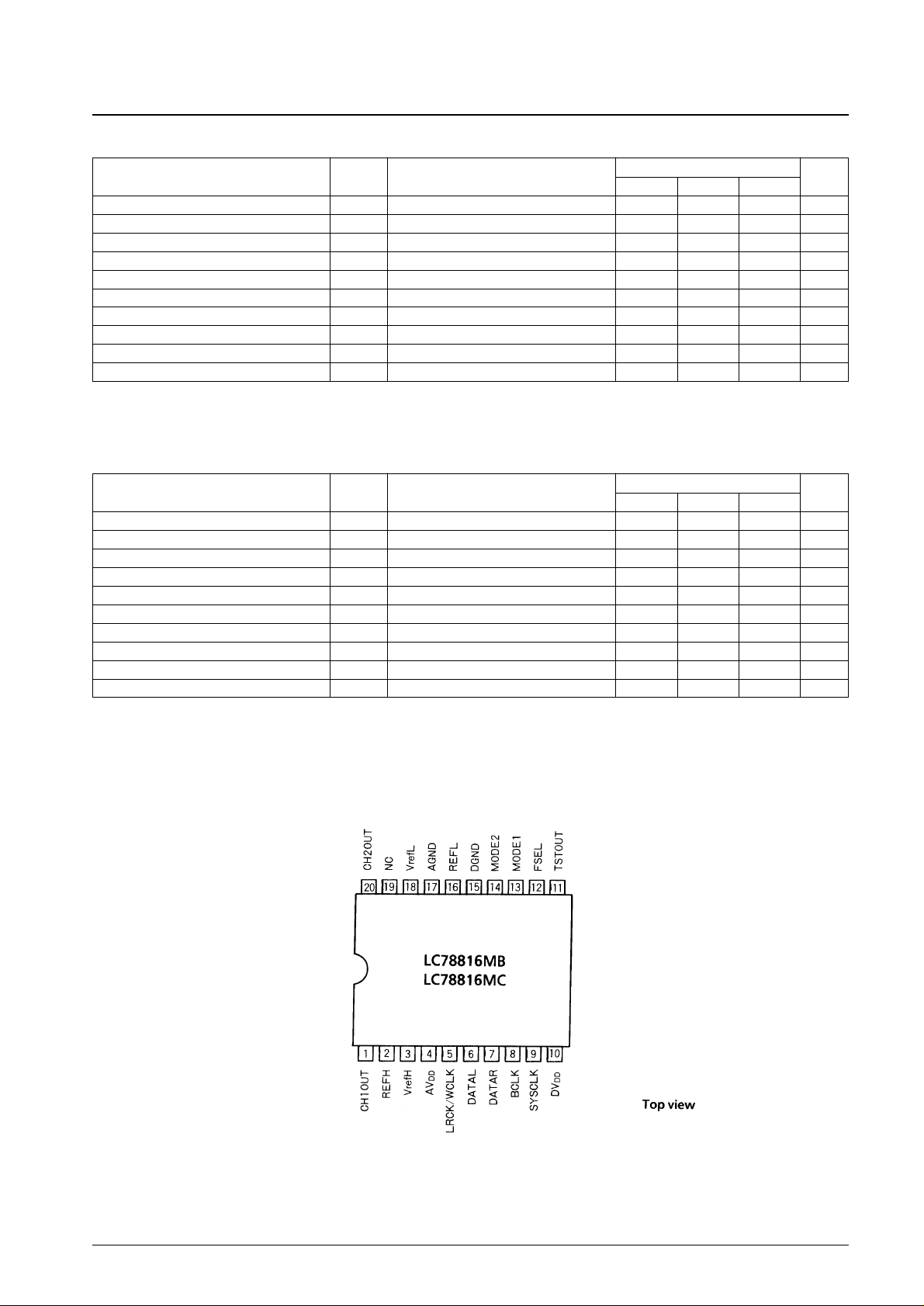
Pin Assignment
No. 4250-4/11
LC78816MB, 78816MC
Block Diagram
Pin No. Pin Name Function and Operational Description
1 CH1OUT Channel 1 output pin (left channel)
2
REFH
Reference voltage high level pin
Normally connected to AGND through a capacitor.
3 VrefH Reference voltage high level input pin
4 AV
DD
Analog system power supply voltage pin
5
LRCK/WCLK
LR clock and word clock input pin
Used to generate the internal signal that latches the digital audio data (DATAL and DATAR).
Digital audio data input pin
6 DATAL
Data is input from the MSB bit serially.
When FSEL is low, channel 1 data is input.
When FSEL is high, channel 1 and channel 2 data are input using time division.
Digital audio data input pin
7 DATAR
Data is input from the MSB bit serially.
When FSEL is low, channel 2 data is input.
When FSEL is high, functions as the interface switching pin.
Bit clock input pin
8 BCLK This is the clock for reading in digital audio data bit serially. Also functions as the IC’s system clock when SYSCLK is
fixed low or high.
System clock input pin
9 SYSCLK This is the system clock that drives the IC. However, in certain modes it is used as the interface switching pin.
(See the timing charts.)
10 DV
DD
Digital system power supply voltage pin
11 TSTOUT Output pin for IC testing
12 FSEL
When low, digital audio data is input simultaneously from the DATAL and DATAR pins.
When high, digital audio data is input from the DATAL pin in time division mode.
13 MODE1
Interface switching pins. (See the timing charts.)
14 MODE2
15 DGND Digital system ground pin
16 REFL
Reference voltage low level pin.
Normally connected to AGND through a capacitor.
17 AGND Analog system ground pin
18 VrefL Reference voltage low level input pin
19 NC No connection
20 CH2OUT Channel 2 output pin (right channel)
Pin Functions
 Loading...