

CMOS LSI
Ordering number : EN5521
13097HA(OT) No. 5521-1/22
SANYO Electric Co.,Ltd. Semiconductor Bussiness Headquarters
TOKYO OFFICE Tokyo Bldg., 1-10, 1 Chome, Ueno, Taito-ku, TOKYO, 110 JAPAN
CD Graphics Decorder
LC7874E
Overview
The LC7874E is a CMOS LSI that provides the signal
processing needed for compact disc graphics (CD-G) on a
single chip. The LC7874E accepts subcode R to W
signals output from a CD player DSP LC786X Series,
LC7862XE Series, or LC7863XE Series device, and
performs de-interleaving, error detection and correction,
graphic instruction processing, and image processing.
Features
• A CD-G decoder can be configured using a three-chip
combination of this LSI—the LC7874E—with external
RAM (64K × 4 bits) and an LC78010E digital RGB
encoder.
• Performs insertion and protection of CD subcode R to
W sync signals and detection of R to W signal deinterleave error signals.
• Has two crystal oscillators, for NTSC and PAL, with
simple switchover by means of a control pin.
Connecting a crystal resonator of 14.31818 MHz for
NTSC and 17.734476 MHz for PAL enables the
standard clock and other necessary timings to be
generated internally.
• Performs CD graphics instruction processing and
drawing functions, and controls image display.
• Has microcomputer interface functions, allowing set
upgrading.
• Provides superimposition support.
• Has a color bar signal output function.
• DRAM interface and RGB output and sync signal output
are 3-state outputs.
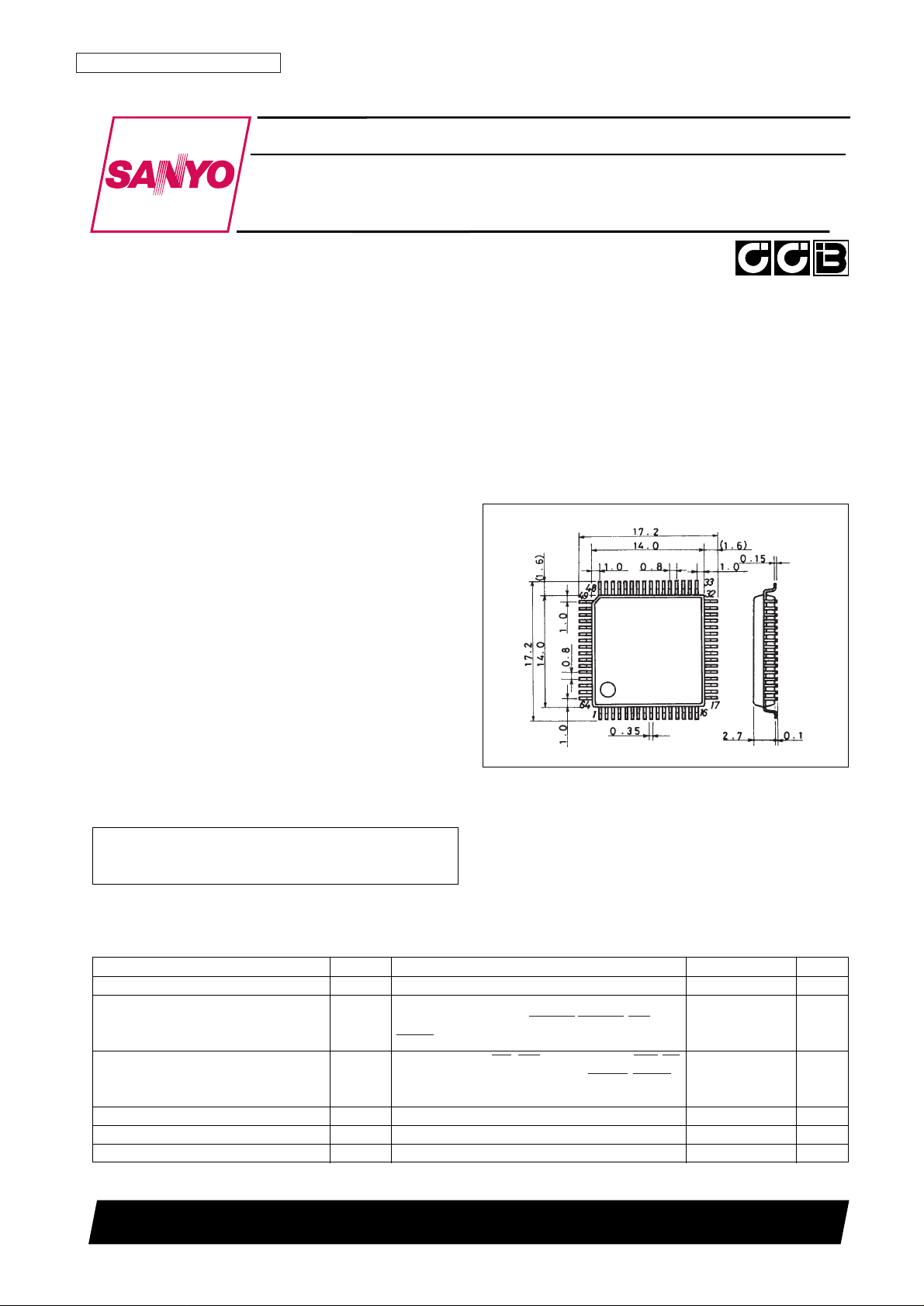
Package Dimensions
unit: mm
3159-QFP64E
SANYO: QIP64E
[LC7874E]
• CCB is a trademark of SANYO ELECTRIC CO., LTD.
• CCB is SANYO’s original bus format and all the bus
addresses are controlled by SANYO.
Parameter Symbol Conditions Ratings Unit
Power supply voltage V
DD
V
DD
V
SS
– 0.3 to V
SS
+ 7.0 V
S1, S2, SFSY, PW, SBSY, CE, DI, CL, MUTE, DB0 to 3,
Input voltage V
IN
CB, CE1, CE2, CE3, LINE, HRESET, VRESET, INIT, V
SS
– 0.3 to V
DD
+ 0.3 V
RESET, N/P, SON, XIN1, XIN2
SBCK, DO, CDGM, WE, RAS, A0 to 7, DB0 to 3, CAS, OE,
Output voltage V
OUT
ROUT0 to 3, GOUT0 to 3, BOUT0 to 3, HSYNC, CSYNC, V
SS
– 0.3 to V
DD
+0 .3 V
BLANK, YS, 4FSCO, EFLG, FSCO, XOUT1, XOUT2
Allowable power dissipation Pd max Ta = 25°C 500 mW
Operating temperature Topr –30 to +85 °C
Storage temperature Tstg –40 to +125 °C
Specifications
Electrical Characteristics at Ta = –30°C to +85°C
No. 5521-2/22
LC7874E
Parameter Symbol Conditions
Ratings
Unit
min typ max
Power supply voltage V
DDVDD
3.0 5.0 5.5 V
V
IH
1 S1, S2, CB LINE, N/P, SON 0.7 V
DD
V
DD
+ 0.3 V
V
IH
2 INIT, RESET 0.8 V
DD
V
DD
+ 0.3 V
Input high-level voltage V
IH
3 CL 0.8 V
DD
5.8 V
V
IH
4 DB0 to DB3, HRESET, VRESET 2.2 V
DD
+ 0.3 V
V
IH
5 SFSY, PW, SBSY, CE, DI, MUTE, CE1 to CE3 2.2 5.8 V
V
IL
1 S1, S2, CB, LINE, N/P, SON V
SS
– 0.3 0.3V
DD
V
Input low-level voltage
V
IL
2 CL, INIT, RESET V
SS
– 0.3 0.2V
DD
V
V
IL
3
SFSY, PW, SBSY, CE, DI, MUTE, DB0 to DB3,
V
SS
– 0.3 0.8 V
CE1 to CE3, HRESET, VRESET
Input frequency
F
SCIN
1 XIN1 14.31818 MHz
F
SCIN
2 XIN2 17.734476 MHz
Input amplitude V
IN
XIN1, XIN2 0.5 V
DD
Vp-p
Allowable Operating Ranges at Ta = –30°C to +85°C
Parameter Symbol Conditions
Ratings
Unit
min typ max
S1, S2, SFSY, PW, SBSY, CE, DI, CL, MUTE,
Input high-level current
I
IH
1 DB0 to DB3, LINE, HRESET, VRESET, CE1 to 3, 5 µA
INIT, RESET, N/P, SON : V
IN
= V
DD
IIH2 CB : VIN= V
DD
30 100 200 µA
S1, S2, SFSY, PW, SBSY, CE, DI, CL, MUTE,
Input low-level current I
IL
1 DB0 to DB3, CB, LINE, HRESET, VRESET, –5 µA
CE1 to 3, INIT, RESET, N/P, SON : V
IN
= V
SS
SBCK, WE, RAS, A0 to 7, CAS, OE, DB0 to 3,
Output high-level voltage V
OH
CDGM, ROUT0 to 3, GOUT0 to 3, BOUT0 to 3,
V
DD
– 1 V
DD
V
FSCO, 4FSCO, HSYNC, YS, CSYNC,
BLANK, EFLG : I
OH
= –0.5 mA
SBCK, WE, RAS, A0 to 7, CAS, OE, DB0 to 3,
Output low-level voltage V
OL
CDGM, ROUT0 to 3, GOUT0 to 3, BOUT0 to 3,
V
SS
0.4 V
FSCO, 4FSCO, HSYNC, YS, CSYNC,
BLANK, EFLG : I
OL
= 2.0 mA
A0 to A7, RAS, CAS, OE, WE, DB0 to DB3,
Output off leakage current I
OFF
HSYNC, ROUT0 to 3, GOUT0 to 3, BOUT0 to 3, –5 +5 µA
CSYNC, BLANK, FSCO, 4FSCO
Built-in feedback resistance R
X
XIN1, XIN2 1 MΩ
Clock frequency f
O
SBCK 220 kHz
Operating current drain I
DD
V
DD
26 40 mA
Electrical Characteristics at Ta = –30 to +85°C, VDD= 5 V unless otherwise specified
No. 5521-3/22
LC7874E
Parameter Symbol Conditions
Ratings
Unit
min typ max
Input minimum pulse width
t
WH
CL, high pulse width 400 ns
t
WL
CL, low pulse width 400 ns
Data setup time t
DS
DI, CL 200 ns
Data hold time t
DH
DI, CL 200 ns
Data hold time t
DOH
DO, CL 130 300 ns
CE wait time t
CP
CE, CL 400 ns
CE setup time t
CS
CE, CL 400 ns
CE hold time t
CH
CE, CL 400 ns
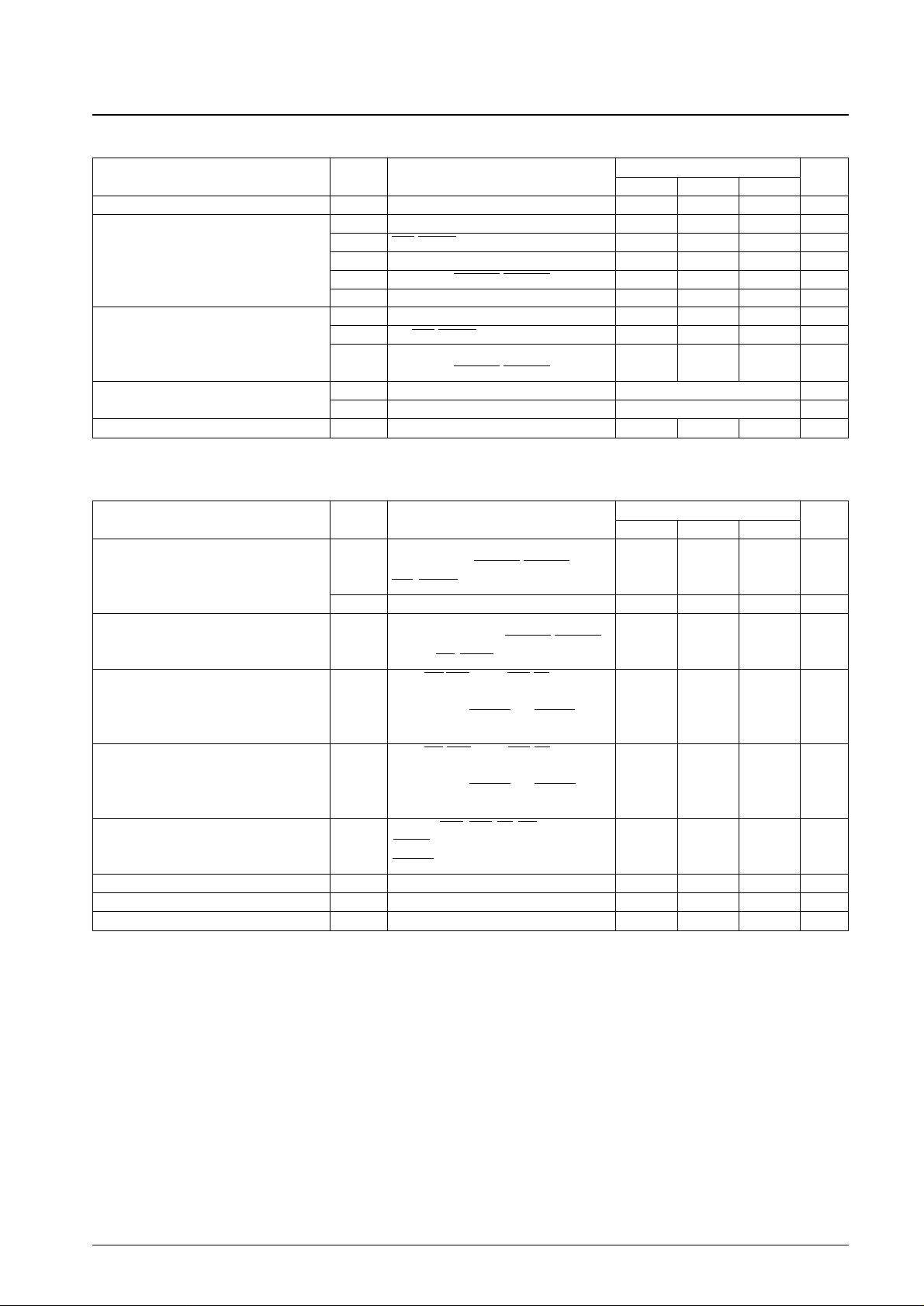
Timing Characteristics (Microcontroller Interface Timing) at Ta = 25°C, VDD= 5 V
No. 5521-4/22
LC7874E
Parameter Symbol Conditions
Ratings
Unit
min typ max
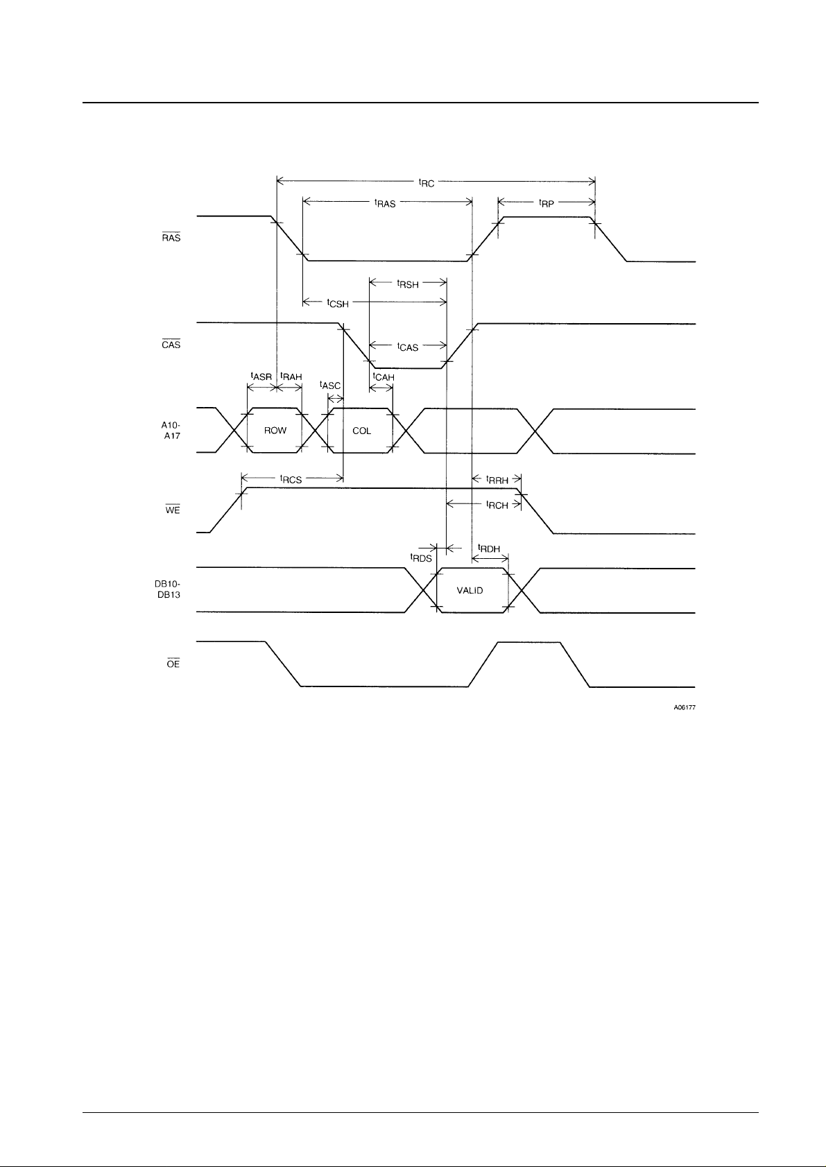
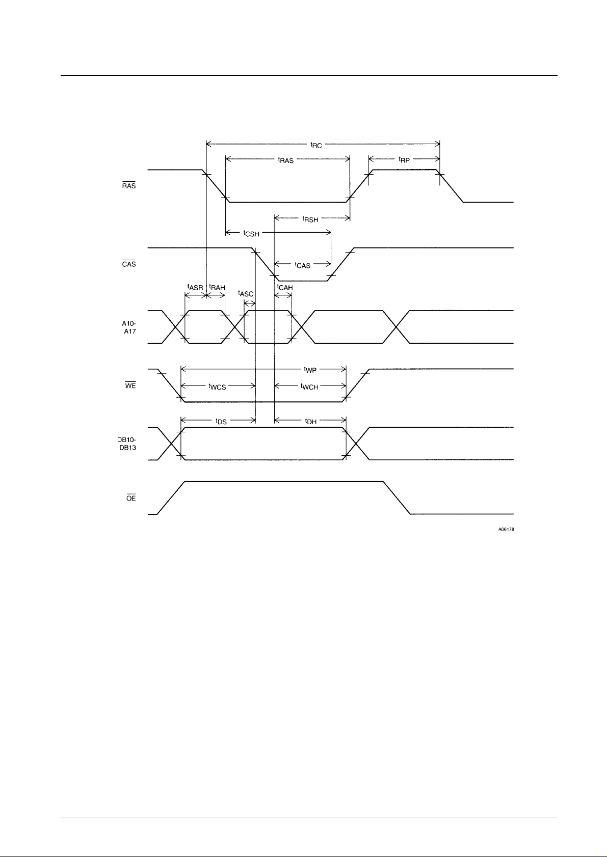
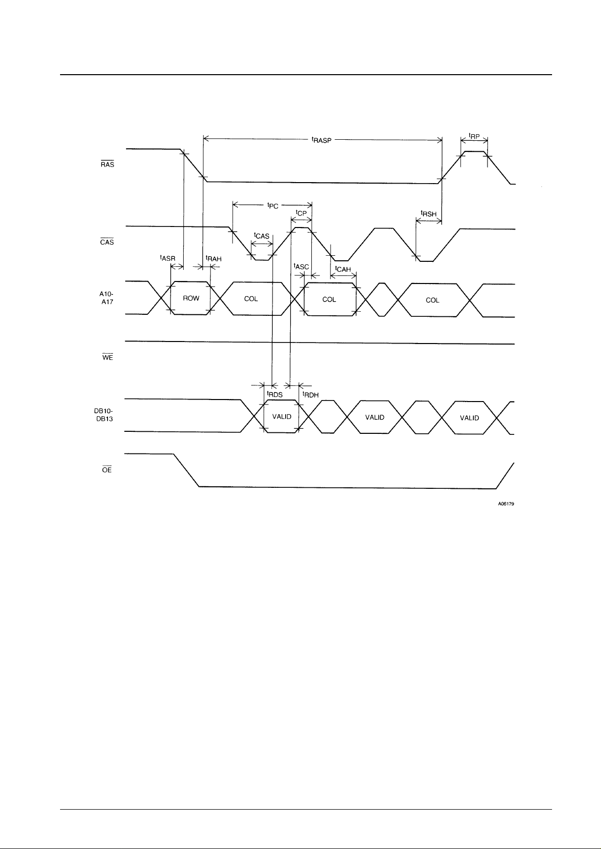
Random read/write cycle time t
RC
250 ns
Page mode cycle time t
PC
130 ns
RAS precharge time t
RP
100 ns
RAS pulse width t
RAS
120 ns
RAS pulse width (page mode) t
RASP
18000 ns
RAS hold time t
RSH
60 ns
CAS hold time t
CSH
120 ns
CAS pulse width t
CAS
60 ns
CAS precharge time t
CPN
50 ns
CAS precharge time t
CP
(In page mode) 50 ns
Row address setup time t
ASR
100 ns
Row address hold time t
RAH
50 ns
Column address setup time t
ASC
0 ns
Column address hold time t
CAH
50 ns
Read command setup time t
RCS
150 ns
Read command hold time t
RCH
(Referenced to CAS ) 120 ns
Read command hold time t
RRH
(Referenced toRAS) 120 ns
Write command setup time t
WCS
100 ns
Write command hold time t
WCH
50 ns
Write command pulse width t
WP
150 ns
Write data setup time t
DS
100 ns
Write data hold time t
DH
100 ns
CAS setup time t
CSR
(CAS before RAS) 50 ns
CAS hold time t
CHR
(CAS before RAS) 50 ns
RAS precharge CAS active time t
RPC
50 ns
Read data setup time t
RDS
20 ns
Read data hold time t
RDH
10 ns
Refresh time t
REF
3.5 ms
Timing Characteristics (DRAM Access Timing) at Ta = 25°C, VDD= 5 V
No. 5521-5/22
LC7874E
DRAM Read Cycle
No. 5521-6/22
LC7874E
DRAM Early Write Cycle
No. 5521-7/22
LC7874E
DRAM Page Mode Read Cycle

No. 5521-8/22
LC7874E
DRAM Page Mode Write Cycle
DRAM CAS-Before-RAS Refresh Cycle

No. 5521-9/22
LC7874E
Pin Assignment

No. 5521-10/22
LC7874E
Pin Functions
Pin Pin Symbol Pin Name I/O Polarity Function
1 S1
CD DSP selection pins In Positive
2 S2
3 SBCK Clock output pin Out — Subcode R to W read clock output
4 SFSY Sync signal input pin In Positive Subcode frame sync signal input (MORE+ input)
5 PW Data input pin In Positive Subcode R to W data input (MORE+ input)
6 SBSY Sync signal input pin In Positive Subcode block sync signal input (MORE+ input)
7 V
DD
Power supply pin (+5 v) — — Digital power supply
8 CE Enable input pin In Positive Serial input/output data control input (MORE+ input)
9 DO Data output pin Out Positive Serial data output (Nch open-drain)
10 DI Data input pin In Positive Serial data input (MORE+ input)
11 CL Clock input pin In Positive Serial data input/output clock input (MORE+ input)
12 MUTE Data input pin In Positive Control signal input invalidating subcode data (MORE+ input)
13 V
SS
Ground pin (GND) — — GND
14 CB Color bar selection pin In Positive L: Normal mode, H: Color bar output (built-in pull-down resistor)
15 CDGM Graphic data discrimination output pin Out Positive
Goes high when graphics data is input (can be reset low by command
control).
16 CE1 DRAM control input pin In Positive
Signal input setting DRAM connection pin to high impedance (MORE+
input)
17 A0 DRAM output pin I/O Positive DRAM address (A0) output
18 A1 DRAM output pin I/O Positive DRAM address (A1) output
19 A2 DRAM output pin I/O Positive DRAM address (A2) output
20 A3 DRAM output pin I/O Positive DRAM address (A3) output
21 A4 DRAM output pin I/O Positive DRAM address (A4) output
22 A5 DRAM output pin I/O Positive DRAM address (A5) output
23 A6 DRAM output pin I/O Positive DRAM address (A6) output
24 A7 DRAM output pin I/O Positive DRAM address (A7) output
25 CAS DRAM output pin 3ST Negative DRAM column address strobe signal output
26 WE DRAM output pin 3ST Negative DRAM data write enable signal output
27 OE DRAM output pin 3ST Negative DRAM data read enable signal output
28 RAS DRAM output pin 3ST Negative DRAM row address strobe signal output
29 DB0 DRAM input/output pin I/O Positive DRAM data (D0) input/output
30 DB1 DRAM input/output pin I/O Positive DRAM data (D1) input/output
31 DB2 DRAM input/output pin I/O Positive DRAM data (D2) input/output
32 DB3 DRAM input/output pin I/O Positive DRAM data (D3) input/output
33 BLANK Blank signal output pin 3ST Positive Video signal blanking period output
34 CSYNC Composite sync output pin 3ST Negative Composite sync signal output
S1 S2 Selected CD DSP
0 0 LC7861N/67
1 0 LC7860K/63
0 1 Setting prohibited
1 1 LC7868/62X/63X
Continued on next page.

No. 5521-11/22
LC7874E
Continued from preceding page.
Pin Pin Symbol Pin Name I/O Polarity Function
35 HSYNC Horizontal synchronization output pin 3ST Negative Horizontal sync signal output
36 ROUT3 R data output pin I/O Positive Video signal R3 data output
37 ROUT2 R data output pin I/O Positive Video signal R2 data output
38 ROUT1 R data output pin I/O Positive Video signal R1 data output
39 ROUT0 R data output pin I/O Positive Video signal R0 data output
40 4FSC
0
Clock output pin 3ST Positive
4 × FSC clock output NTSC: 14.31818 MHz
PAL: 17.734476 MHz
41 FSC
0
Clock output pin 3ST Positive
Subcarrier clock output NTSC: 3.579545 MHz
PAL: 4.433619 MHz
42 GOUT3 G data output pin I/O Positive Video signal G3 data output
43 GOUT2 G data output pin I/O Positive Video signal G2 data output
44 GOUT1 G data output pin I/O Positive Video signal G1 data output
45 GOUT0 G data output pin I/O Positive Video signal G0 data output
46 BOUT3 B data output pin I/O Positive Video signal B3 data output
47 BOUT2 B data output pin I/O Positive Video signal B2 data output
48 BOUT1 B data output pin I/O Positive Video signal B1 data output
49 BOUT0 B data output pin I/O Positive Video signal B0 data output
50 CE2 Video output control input pin In Positive
Signal input setting video output pin to high impedance
(MORE+ input)
51 CE3 Sync signal control input pin In Positive
Signal input setting sync signal output pin to high impedance
(MORE+ input)
52 YS Superimposition output pin Out Positive Superimposition control output
53 EFLG Error status monitor output pin Out Positive Error status monitor signal output
54 HRESET External horizontal synchronization input pin In Negative External horizontal synchronization timing control pin
Line number selection input
55 LINE Line number selection pin In — NTSC : L = 263H, H = 262H
PAL : H = 312H, L = 314H
56 VRESET External vertical synchronization input pin In Negative External vertical synchronization timing control pin
57 INIT Initial input pin In Negative System initial signal input
58 RESET Reset input pin In Negative System reset signal input
59 N/P NTSC/PAL selection input pin In Positive
NTSC/PAL selection input
L: NTSC, H: PAL
60 SON Superimposition control pin In Positive
Superimposition ON/OFF control input
H: Superimposition ON
61 XIN2
Crystal oscillator connection pins
In —
PAL crystal oscillator connection pin (4Fsc = 17.734476 MHz)
62 XOUT2 Out —
63 XIN1
Crystal oscillator connection pins
In —
NTSC crystal oscillator connection pin (4Fsc = 14.31818 MHz)
64 XOUT1 Out —

No. 5521-12/22
LC7874E
Block Diagram

No. 5521-13/22
LC7874E
CD-G Instructions
The contents of instructions in the CD Red Book which are supported by the LC7874E are as follows.
ZERO mode (MODE = 0, ITEM = 0)
LINE GRAPHICS mode (MODE = 1, ITEM = 0)
①
INSTRUCTION (4): Write FONT
②
INSTRUCTION (12): Write Scroll SCREEN
TV GRAPHICS mode (MODE = 1, ITEM = 1)
①
INSTRUCTION (1): Preset MEMORY
②
INSTRUCTION (2): Preset BORDER
③
INSTRUCTION (6): Write FONT FOREGROUND/BACKGROUND
④
INSTRUCTION (20): scroll SCREEN with preset
⑤
INSTRUCTION (24): scroll SCREEN with copy
⑥
INSTRUCTION (30): Load CLUT color-0 color-7
⑦
INSTRUCTION (31): Load CLUT color-8 color-15
⑧
INSTRUCTION (38): EXCLUSIVE-OR FONT
Outline of Functions
1. Crystal clock oscillation: XIN1, XOUT1, XIN2, XOUT2, N/P, 4FSCO, FSCO
XIN1 and XOUT1 are 14.31818 MHz (NTSC) crystal oscillator connection pins, and XIN2 and XOUT2 are
17.734476 MHz (PAL) crystal oscillator connection pins. Both modes can be supported by switching the N/P pin.
The 4FSCO pin outputs the Xtal OSC clock, and the FSCO pin outputs this clock divided by 4. The pin functions in
each mode are shown below.
2. Subcode interface: S1, S2, SBCK, SFSY, PW, SBSY
Control of the S1 and S2 pins provides interfacing with the following three modes. Driving the mute pin high
disables SBSY and PW input and SBCK output.
XIN1, XOUT1 XIN2, XOUT2 N/P TV system 4FSCO FSCO
14.31818 MHz * L NTSC/M 14.31818 MHz 3.579545 MHz
* 17.734476 MHz H PAL/GBIDH 17.734476 MHz 4.433619 MHz
S1 S2 Mode
L L LC7861N/67 interface
H L LC7860K/63 interface
H H LC78681/62X/63X interface

No. 5521-14/22
LC7874E
With the LC7860K/63 interface, SBCK is transmitted when SFSY is confirmed to be low approximately 2.2 µs after a
falling edge of SFSY is detected. With other interfaces, SBCK is transmitted when SFSY is confirmed to be high and
SBSY to be low approximately 2.2 µs after a rising edge of SFSY is detected.
(1) LC7860 interface [DSP pin names shown in parentheses]
(2) LC7861N/67 interface [DSP pin names shown in parentheses]
(3) LC78681/62X/63X Series interface
Same as (2), except that the SBCK polarity is shifted inversely (shifted on rise of SBCK).
3. DRAM interface
Interface pins: A0 to A7, DB0 to DB3, RAS, CAS, WE, OE
64K × 4-bit DRAM is connected externally. The interface pins are set to high impedance by driving the CE1 pin
high. MPEG DRAM sharing is possible.
4. CD graphic monitor pin: CDGM
CDGM goes high once the LC7874E accepts any CD-G instruction. In the power-on state, once CDGM goes high it
remains high. It can be driven low by driving the INIT pin low or transferring an INIT command from the
microcontroller.

No. 5521-15/22
LC7874E
5. Display format
6. Video output: ROUT0 to ROUT3, GOUT0 to GOUT3, BOUT0 to BOUT3
7. Error flag output: EFLG
Error detection results can be monitored with the EFLG pin.

No. 5521-16/22
LC7874E
8. Color bar output: CB
When the CB pin is driven high, color bars are output from the video output pins. Details of the color bars are shown
below.
Drawing Functions (Graphic Functions)
1. Operating modes (scan operation, display operation)
NTSC mode
• Non-interlace 60 Hz (262 or 263 lines)
• Dot clock 2fsc: 7.15909 MHz (T = 139.67 ns)
• System clock 4fsc: 14.31818 MHz
PAL mode
• Non-interlace 50 Hz (312 or 314 lines)
• Dot clock 4fsc × 2/5: 7.09379 MHz (T = 140.97 ns)
• System clock 4fsc: 17.734476 MHz
PAL60 mode
• Non-interlace 60 Hz (262 or 263 lines)
• Dot clock 4fsc × 2/5: 7.09379 MHz (T = 140.97 ns)
• System clock 4fsc: 17.734476 MHz
2. Display functions
• Display resolution 288 dots × 192H
• Image data area 300 dots × 216H
• 16-color display Selection of 16 colors from 4096
Microcontroller Interface (CCB)
1. Transfer format (for command transfer)
Transfer format (example)
R G B
➀ White F F F
➁ Gray B B B
➂ Yellow F F O
➃ Cyan O F F
➄ Green O F O
➅ Magenta F O F
➆ Red F O O
➇ Blue O O F
BORDER (BLACK) O O O

No. 5521-17/22
LC7874E
Display Control Command Table
First byte Second byte
Command
MSB
Command identification code
LSB
MSB Data LSB
7 6 5 4 3 2 1 0 7 6 5 4 3 2 1 0
Register 00HEX
0 0 0 0 0 0 0 0 INIT SCP
2
SCP1SCP0CB
DISK TV/ VRAM
(Various mode settings) /GPH LINE /BG
Register 10HEX
0 0 0 1 0 0 0 0 VP3VP2VP1VP0HP3HP2HP1HP
0
(Fine adjustment of screen position)
Register 20HEX
0 0 1 0 0 0 0 0 CH
7
CH6CH5CH4CH3CH2CH1CH
0
(Channel 0 to 7 ON/OFF)
Register 30HEX
0 0 1 1 0 0 0 0 CH
15
CH14CH13CH12CH11CH10CH9CH
8
(Channel 8 to 15 ON/OFF)
Register 40HEX
0 1 0 0 0 0 0 0 BGG
3
BGG2BGG1BGG0BGR3BGR2BGR1BGR
0
(BGC R, G settings)
Register 50HEX
0 1 0 1 0 0 0 0 0 0 0 0 BGB
3
BGB2BGB1BGB
0
(BGC B setting)
Register 60HEX
0 1 1 0 0 0 0 0 CKG3 CKG2 CKG1 CKG0 CKR3 CKR2 CKR1 CKR0
(Chroma key color R, G settings)
Register 70HEX
0 1 1 1 0 0 0 0 0 0 0 0 CKB3 CKB2 CKB1 CKB0
(Chroma key color B setting)
Register 80HEX
1 0 0 0 0 0 0 0
CSY PAL
0 YT4 YT3 YT2 YT1 YT0
(YS output phase adjustment) SEL 60
Register 90HEX
1 0 0 1 0 0 0 0
CV
MVMD EXSN HVMK 0 TST2 TST1 TST0
(External synchronization mode, test mode) SEL
Register A0HEX
1 0 1 0 0 0 0 0 0 0 0 SCV4 SCV3 SCV2 SCV1 SCV0
(Subtitle scroll: vertical)
Register B0HEX
1 0 1 1 0 0 0 0 0 0 SCH5 SCH4 SCH3 SCH2 SCH1 SCH0
(Subtitle scroll: horizontal)
Register 01HEX
0 0 0 0 0 0 0 1 R S T U V W 0 0
(19-byte command input)

No. 5521-18/22
LC7874E
Description of Commands
Command transmission should be performed LSB-first.
1. Control item code 00HEX: Various mode settings
Default: MSB [01100000] LSB
Data 0: VRAM/BG Display screen switchover setting
0: VRAM contents displayed
1: Background color displayed
Data 1: TV/LINE Graphic display mode setting
0: TV graphic mode
1: LINE graphic mode
Data 2: DISK/GPH Disk command acceptance control
0: DISK command only accepted
1: DISK command acceptance ignored, MGC (Micro graphic command) only accepted
Data 3: CB Color bar screen output setting
0: Graphic signal output
1: Color bar signal output
Data 4: SCP0 YS output (pin 52) control
Data 5: SCP1 Superimposition compare condition (valid only when SON = 1: pin 60)
Data 6: SCP2 YS output (pin 52) control
0: When SCP0, SCP1 = 0, 0; 0, 1, and compare condition is not satisfied, setting is full-screen low
(transparent)
1: L: When SCP0, SCP1 = 0, 0; 0, 1, and compare condition is not satisfied, setting is full-screen high
(display)
Data 7: INIT Software reset setting
0: Internal reset not executed (normal)
1: Internal reset executed (display screen becomes blue background screen)
2. Control item code 10
HEX
: Fine adjustment of screen position
Default: MSB [00000000] LSB
Data 0: HP0 Horizontal fine adjustment of screen position
Data 1: HP1 Specified as two’s complement with left as positive direction
Data 2: HP2 (variable by –16 to +14 dots from center in 2-dot units)
Data 3: HP3
Data 4: VP0 Vertical fine adjustment of screen position
Data 5: VP1 Specified as two’s complement with up as positive direction
Data 6: VP2 (variable by –16 to +14 dots from center in 2-dot units)
Data 7: VP3
SCP1 SCP0 Compare condition
0 0 Comparison not performed
1 0
When border color is black, YS is high (display) in the parts whose color does
not match the border color, and low (transparent) otherwise
1 1 High in parts whose color does not match the chroma key color; low otherwise

No. 5521-19/22
LC7874E
3. Control item code 20
HEX
: Channel on/off setting
Default: MSB [00000011] LSB
Data 0: CH0 CH0 to CH7 on/off setting
Data 1: CH1
Data 2: CH2 0: Channel off
Data 3: CH3 1: Channel on
Data 4: CH4
Data 5: CH5
Data 6: CH6
Data 7: CH7
4. Control item code 30
HEX
: Channel on/off setting
Default: MSB [00000000] LSB
Data 0: CH8 CH8 to CH15 on/off setting
Data 1: CH9
Data 2: CH10 0: Channel off
Data 3: CH11 1: Channel on
Data 4: CH12
Data 5: CH13
Data 6: CH14
Data 7: CH15
5. Control item code 40
HEX
: BGC color (R, G) settings
Default: MSB [00000000] LSB
Data 0: BCR0 BGC color: R setting = 16 kinds
Data 1: BCR1
Data 2: BCR2
Data 3: BCR3
Data 4: BCG0 BGC color: G setting = 16 kinds
Data 5: BCG1
Data 6: BCG2
Data 7: BCG3
6. Control item code 50
HEX
: BGC color (B) setting
Default: MSB [00001010] LSB
Data 0: BCB0 BGC color: B setting = 16 kinds
Data 1: BCB1
Data 2: BCB2
Data 3: BCB3 * R, G, B, 16 kinds each; selection of 1 color from 4096
Data 4 to data 8: Fixed at 0
7. Control item code 60
HEX
: Chroma key color (R, G) settings
Default: MSB [00000000] LSB
Data 0: CKR0 Chroma key color: R setting = 16 kinds
Data 1: CKR1
Data 2: CKR2
Data 3: CKR3
Data 4: CKG0 Chroma key color: G setting = 16 kinds
Data 5: CKG1
Data 6: CKG2
Data 7: CKG3

No. 5521-20/22
LC7874E
8. Control item code 70
HEX
: Chroma key color (B) setting
Default: MSB [00000000] LSB
Data 0: CKB0 Chroma key color: B setting = 16 kinds
Data 1: CKB1
Data 3: CKB3 * R, G, B, 16 kinds each; selection of 1 color from 4096
Data 4 to data 8: Fixed at 0
9. Control item code 80
HEX
: YS signal output/video signal output phase adjustment data setting
Default: MSB [00000000] LSB
Data 0: YT0 YS signal output/video signal output phase adjustment data
Data 1: YT1
Data 2: YT2
Data 3: YT3
Data 4: YT4
Data 5: Fixed at 0
Data 6: PAL60 PAL/PAL60 setting (valid only when N/P = 1)
0: PAL
1: PAL60
Data 7: CSYSEL CSYNC output addressing (autonomous mode only)
0: Equalization pulses used
1: No equalization pulses
10. Control item code 90
HEX
: External synchronization control, test mode setting
Default: MSB [00000000] LSB
Data 0: TST0 Test mode addressing (normally fixed low)
Data 1: TST1
Data 2: TST2
Data 3: Fixed at 0
Data 4: HVMK HRESET, VRESET mask
0: Mask used
1: No mask
Data 5: EXSN Sync signal rest control setting when using external clock (when SON = 1)
0: Reset executed with HRESET (pin 54) and VRESET (pin 56) signals
0: Reset executed with VRESET (pin 56) signal (HRESET signal unnecessary)
Data 6: MVMD Moving display area setting
0: Movement of display area only
1: Border area included in movement (only horizontal movement possible)
Data 7: CVSEL CSYNC output pin setting
0: CSYNC output
1: VSYNC output
11. Control item code A0
HEX
: Superimposed text scroll amount, vertical setting
Default: MSB [00000000] LSB
Data 0: SCV0 Upward scroll amount (font unit) setting (scroll amount: 0 to 17 font units)
Data 1: SCV1 Screen display position scrolled vertically by 1 font unit
Data 2: SCV2 (1 font unit: 12 vertical dots (12H))
Data 3: SCV3
Data 4: SCV4
Data 5 to data 7: Fixed at 0

No. 5521-21/22
LC7874E
12. Control item code C0
HEX
: Superimposed text scroll amount, horizontal setting
Default: MSB [00000000] LSB
Data 0: SCH0 Left scroll amount (font unit) setting (scroll amount: 0 to 49-font units)
Data 1: SCH1 Screen display position scrolled horizontally in 1-font unit
Data 2: SCH2 (1-font unit: 6 horizontal dots)
Data 3: SCH3
Data 4: SCH4
Data 5: SCH5
Data 6, data 7: Fixed at 0
13. Control item code 01
HEX
: 19-byte command input (MGC write)
Transfer format
①
Address: F4
HEX
②
Control item: 01
HEX
③
sym0 to sym19: R to W = subcode input
④
Executed on fall
14. Control item code 11
HEX
: 19-byte command input (pack data read)
Transfer format
①
Address: F5
HEX
②
Data (check flags)
MSB [PF1, PF0, QF1, QF0, DKMD, VBLK, EXEC, OE] :LSB
Data 0: OE 1 when the next 18 bytes are guaranteed and are the first data to be read.
* Note: Reading must be completed within 1.1 ms after OE output setting.
Data 1: EXEC Command status
0: Command executing
1: Command wait state
Data 2: VBLK 1 output during vertical blanking (vertical retrace line) period
Vertical retrace line period NTSC: 19H
PAL: 25H
Data 3: DKMD Disk identification flag
0: CD
1: CD-G

No. 5521-22/22
LC7874E
Data 4: QF0 QF0 error correction Q flag data
Data 5: QF1 QF1 error correction Q flag data
Data 6: PF0 PF0 error correction P flag data
Data 7: PF1 PF1 error correction Q flag data
③
sym0, 1, 4 to 19: R to W = subcode input
MSB [R, S, T, U, V, W, 0, 0] LSB
Sample Application Circuit : NTSC
This catalog provides information as of January, 1997. Specifications and information herein are subject to
change without notice.
■ No products described or contained herein are intended for use in surgical implants, life-support systems, aerospace
equipment, nuclear power control systems, vehicles, disaster/crime-prevention equipment and the like, the failure of
which may directly or indirectly cause injury, death or property loss.
■ Anyone purchasing any products described or contained herein for an above-mentioned use shall:
➀
Accept full responsibility and indemnify and defend SANYO ELECTRIC CO., LTD., its affiliates, subsidiaries and
distributors and all their officers and employees, jointly and severally, against any and all claims and litigation and all
damages, cost and expenses associated with such use:
➁
Not impose any responsibility for any fault or negligence which may be cited in any such claim or litigation on
SANYO ELECTRIC CO., LTD., its affiliates, subsidiaries and distributors or any of their officers and employees
jointly or severally.
■ Information (including circuit diagrams and circuit parameters) herein is for example only; it is not guaranteed for
volume production. SANYO believes information herein is accurate and reliable, but no guarantees are made or implied
regarding its use or any infringements of intellectual property rights or other rights of third parties.
 Loading...