

Ordering number : EN4868A
O3097HA (OT)/20695TH (OT) No. 4868-1/17
SANYO Electric Co.,Ltd. Semiconductor Bussiness Headquarters
TOKYO OFFICE Tokyo Bldg., 1-10, 1 Chome, Ueno, Taito-ku, TOKYO, 110 JAPAN
CD Graphics Decoder
LC7872E
CMOS LSI
Overview
The LC7872E is a CMOS LSI that integrates in a single
chip the signal processing functions required for compact
disk graphics (CD-G) decoding. The LC7872E accepts the
subcode R to W signals output by a CD-DSP chip such as
the Sanyo LC786X series, LC7862XE series or
LC7863XE series and performs de-interleaving, error
detection and correction, graphics instruction processing
and image processing.
Functions
• Built-in RGB encoder allows a CD-G decoder to be
implemented in just two chips: the LC7872E and an
external 64-kword × 4-bit DRAM
• Interpolation and protection for the CD subcode
synchronization signals as well as de-interleaving, error
detection and correction for the R to W signals.
• Two crystal oscillator systems, one for NTSC and one
for PAL are provided and can be switched easily using
the control pin provided. The standard clock and all
required internal timings can be generated by
connecting a 14.31818 MHz crystal for NTSC and/or a
17.734476 MHz crystal for PAL.
• The LC7872E performs CD graphics instruction
processing and drawing processing and controls the
image display.
• Composition video 8-bit D/A converter output provided
• Superimposition support
• Microprocessor interface provided to support set
upgrades.
• Define transparency support
• Color bar output function
Features
• A CD-G decoder can be implemented with just two
chips: a controller is not required.
• Silicon gate CMOS structure for low power operation
• Single 5 V power supply
• 64-pin QFP (QIP) package
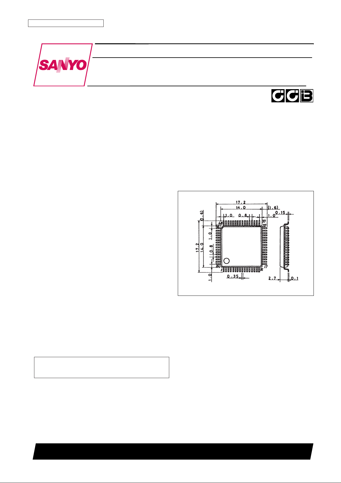
Package Dimensions
unit: mm
3159-QFP64E
• CCB is a trademark of SANYO ELECTRIC CO., LTD.
• CCB is SANYO’s original bus format and all the bus
addresses are controlled by SANYO.
[LC7872E]
SANYO: QFP64E
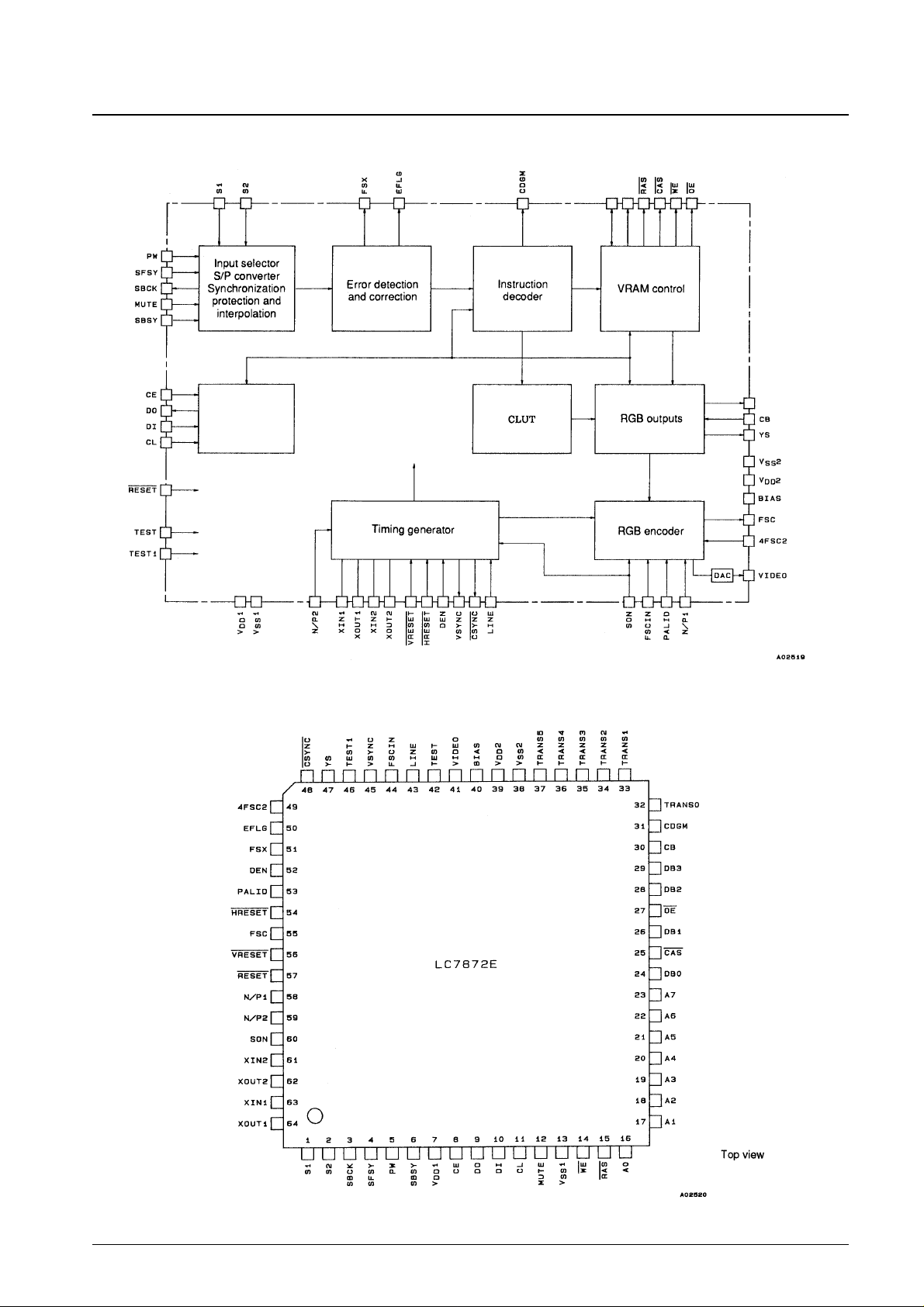
Block Diagram
Pin Assignment
No. 4868-2/17
LC7872E
Microcontroller
interface
DB0 to DB3
A0 to A7
TRANS0 to TRANS5
Specifications
Absolute Maximum Ratings at Ta = 25°C, VSS= 0 V
Allowable Operating Ranges at Ta = 25°C, VSS= 0 V
Electrical Characteristics at Ta = 25°C, VSS= 0 V, VDD= 5 V
No. 4868-3/17
LC7872E
Parameter Symbol Conditions Ratings Unit
Maximum supply voltage V
DD
max VSS– 0.3 to +7.0 V
Maximum input voltage V
IN
max VSS– 0.3 to VDD+ 0.3 V
Maximum output voltage V
OUT
max VSS– 0.3 to VDD+ 0.3 V
Allowable power dissipation Pd max 300 mW
Operating temperature Topr –30 to +85 °C
Storage temperature Tstg –40 to +125 °C
Parameter Symbol Conditions min typ max Unit
Supply voltage V
DD
VDD1, VDD2 4.5 5.5 V
V
IH
(1) RESET 0.7 V
DD
V
DD
V
Input high level voltage
V
IH
(2)
SFSY, PW, SBSY, CE, DI, CL, MUTE, DB0 to DB3,
2.2 V
DD
V
PALID, HRESET, VRESET, N/P1, N/P2, SON
V
IH
(3) S1, S2, CB, TEST, TEST1, LINE, DEN 0.8 V
DD
V
DD
V
V
IL
(1) RESET V
SS
0.3 V
DD
V
Input low level voltage
V
IL
(2)
SFSY, PW, SBSY, CE, DI, CL, MUTE, DB0 to DB3,
V
SS
0.8 V
PALID, HRESET, VRESET, N/P1, N/P2, SON
V
IL
(3) S1, S2, CB, TEST, TEST1, LINE, DEN V
SS
0.2 V
DD
V
High level clock pulse width t
øH
CL: Figure 1 400 ns
Low level clock pulse width t
øL
CL: Figure 1 400 ns
Data setup time t
DS
CL, DI: Figure 1 200 ns
Data hold time t
DH
CL, DI: Figure 1 200 ns
CE wait time t
CP
CE, CL: Figure 1 400 ns
CE setup time t
CS
CE, CL: Figure 1 400 ns
CE hold time t
CH
CE, CL: Figure 1 400 ns
DO setup time t
DOS
CL, DO: Figure 1 130 300 ns
fin (1) XIN1 14.31818 MHz
fin (2) XIN2 17.734476 MHz
Input frequency fin (3) 4FSC2
NTSC mode 14.31818 MHz
PAL mode 17.734476 MHz
fin (4) FSCIN
NTSC mode 3.58 MHz
PAL mode 4.43 MHz
Input amplitude V
IN
XIN1, XIN2, 4FSC2, FSCIN:
0.3 5 Vp-p
sine wave, capacitive coupling
Reset pulse width t
WRES
RESET 400 ns
Parameter Symbol Conditions min typ max Unit
Current drain
I
DD
(1) VDD1 24 40 mA
I
DD
(2) VDD2 12 20 mA
S1, S2, SFSY, PW, SBSY, CE, DI, CL, MUTE, LINE,
Input high level current
IIH(1) HRESET, VRESET, N/P1, N/P2, RESET, SON: 5 µA
V
IN
= V
DD
IIH(2) CB, TEST, TEST1, DEN: VIN= V
DD
30 100 200 µA
S1, S2, SFSY, PW, SBSY, CE, DI, CL, MUTE, LINE,
Input low level current
VIL(1) HRESET, VRESET, N/P1, N/P2, RESET, SON: –5 µA
V
IN
= V
SS
VIL(2) PALID: VIN= V
SS
–200 –100 –30 µA
SBCK, WE, RAS, CAS, OE, A0 to A7, DB0 to DB3,
Output high level voltage V
OH
CDGM, TRANS0 to TRANS5, VSYNC, YS, CSYNC, VDD– 1 V
DD
V
EFLG, FSX, FSC: I
O
= –0.5 mA
Continued on next page.
Continued from preceding page.
No. 4868-4/17
LC7872E
Parameter Symbol Conditions min typ max Unit
SBCK, WE, RAS, CAS, OE, A0 to A7, DB0 to DB3,
Output low level voltage
VOL(1) CDGM, TRANS0 to TRANS5, VSYNC, YS, CSYNC, V
SS
0.4 V
EFLG, FSX, FSC: I
O
= 2 mA
V
OL
(2) DO: IO= 5 mA V
SS
0.75 V
Output off leakage current I
OFF
DO, DB0 to DB3 –5 +5 µA
Built-in feedback resistance R
X
XIN1, XIN2, 4FSC2, FSCIN 1 MΩ
8-bit D/A converter
V
REF
VIDEO 2.40 2.45 2.50 V
reference voltage
8-bit D/A converter
R
DA
VIDEO 300 Ω
output resistance
8-bit D/A converter output level V
DAC
VIDEO: Figure 9
Random read/write cycle time t
RC
Figures 2 and 3 250 ns
Page mode cycle time t
PC
Figures 4 and 5 130 ns
RAS access time t
RAC
Figure 2 210 ns
CAS access time t
CAC
Figures 2 and 4 10 ns
Output turn-off delay time t
OFF
Figures 2 and 4 20 ns
RAS precharge time t
RP
Figures 2, 3, 4, 5 and 6 100 ns
RAS pulse width t
RAS
Figures 2, 3 and 6 120 ns
RAS pulse width (page mode) t
RASP
Figures 4 and 5 18000 ns
RAS hold time t
RSH
Figures 2, 3, 4 and 5 60 ns
CAS hold time t
CSH
Figures 2 and 3 120 ns
CAS pulse width t
CAS
Figures 2, 3, 4 and 5 60 ns
CAS precharge time t
CPN
Figure 6 50 ns
CAS precharge time (page mode) t
CP
Figures 4 and 5 50 ns
Row address setup time t
ASR
Figures 2, 3, 4 and 5 100 ns
Row address hold time t
RAH
Figures 2, 3, 4 and 5 50 ns
Column address setup time t
ASC
Figures 2, 3, 4 and 5 0 ns
Column address hold time t
CAH
Figures 2, 3, 4 and 5 50 ns
Read command setup time t
RCS
Figure 2 150 ns
Read command hold time
t
RCH
Figure 2 120 ns
(referenced to CAS)
Read command hold time
t
RRH
Figure 2 120 ns
(referenced to RAS)
Write command setup time t
WCS
Figure 3 100 ns
Write command hold time t
WCH
Figure 3 50 ns
Write command pulse width t
WP
Figure 3 150 ns
Write data setup time t
DS
Figure 3 100 ns
Write data hold time t
DH
Figure 3 100 ns
CAS setup time (CAS before RAS) t
CSR
Figure 6 50 ns
CAS hold time (CAS before RAS) t
CHR
Figure 6 50 ns
RAS precharge · CAS active time t
RPC
Figure 6 50 ns
Video setup time t
VS
Superimposition: Figure 7 20 25 ns
SBCK output delay time t
SD
NTSC mode: Figure 8 4.74 5.03 µs
PAL mode: 4.79 5.08 µs
SBCK cycle frequency f
SC
NTSC mode: Figure 8 224 kHz
PAL mode: 222 kHz
PW setup time t
PWS
Figure 8 100 ns
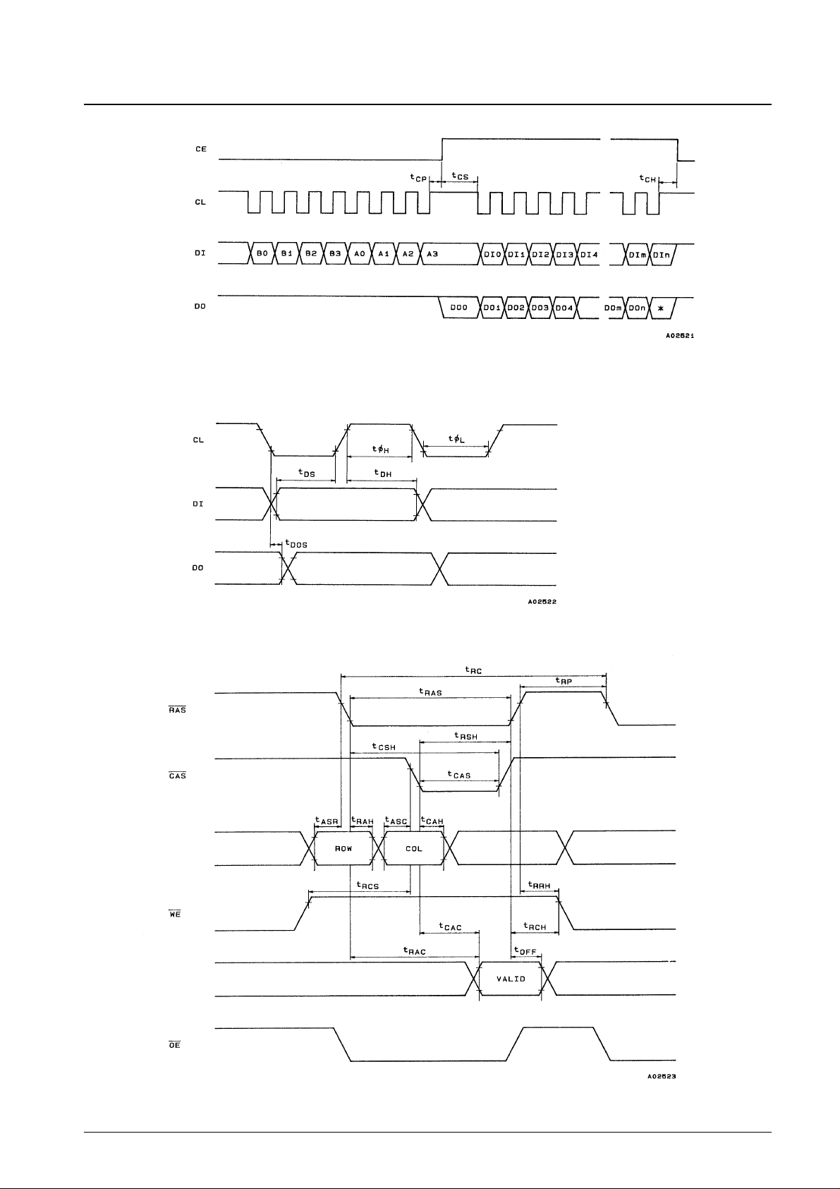
Figure 1 Microcontroller Interface Timing
Figure 2 DRAM Read Cycle
No. 4868-5/17
LC7872E
A0 to A7
DB0 to DB3
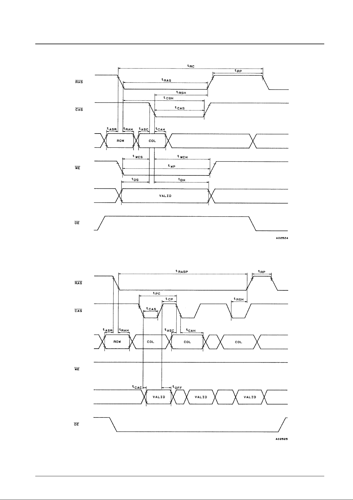
Figure 3 DRAM Early Write Cycle
Figure 4 DRAM Page Mode Read Cycle
No. 4868-6/17
LC7872E
A0 to A7
DB0 to DB3
A0 to A7
DB0 to DB3
 Loading...