

Page 1
Ordering number : EN4861
51795TH (OT) No. 4861-1/19
Overview
The LC7871E and LC7871NE are CMOS LSIs that
integrate the signal processing functions required for
compact disk extended graphics (CD-EG) decoding in a
single chip. These products accept the R to W subcode
signals output by CDP-DSP products such as the
LC7860KA, LC7867E, LC7868E, LC7869E, or
LC78681E, and perform de-interleaving, error detection
and correction, graphics instruction processing, and image
processing.
Functions
• The LC7871E and LC7871NE allow a CD-EG decoder
to be constructed with only three chips with the addition
of two external DRAMs (64k × 4). (An RGB encoder is
provided on chip.)
• The LC7871E and LC7871NE perform subcode
synchronization signal interpolation and protection.
They also perform R to W signal de-interleaving and
error detection and correction.
• These products include two crystal oscillator systems
(one for NTSC and one for PAL) which can be easily
switched from a control pin. These products generate the
reference clocks as well as all internal timings for these
two standards by using a 14.31818 MHz crystal for
NTSC and a 17.734476 MHz crystal for PAL.
• Control of image display using CD graphics instructions
and display processing.
• Composite video 8-bit D/A converter output as well as
“define-transparency” 6-bit D/A converter output.
• Support for superimposition
• Microprocessor interface function that supports endproduct upgrades.
• External input pin for channel selection
• Built-in 6-bit RGB D/A converters
• The only difference between the LC7871E and the
LC7871NE is in the BGC to VRAM transfer.
The LC7871E uses a preset memory instruction for
transfer to VRAM, whereas the LC7871NE uses the
load CLUT instruction.
Features
• A CD-G decoder can be constructed from only two
chips, since no controller is required.
• A CD-EG decoder can be constructed with the addition
of two 256-kbit DRAMs since no controller is required.
• Silicon gate CMOS process for low power dissipation
• 5 V single voltage power supply
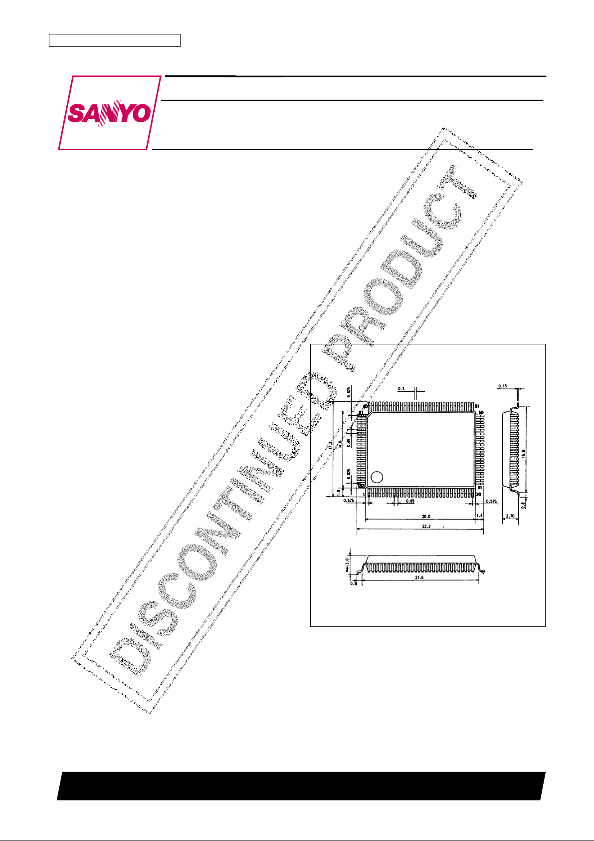
Package Dimensions
unit: mm
3151-QFP100E
SANYO: QIP100E
[LC7871E, 7871NE]
LC7871E, 7871NE
SANYO Electric Co.,Ltd. Semiconductor Bussiness Headquarters
TOKYO OFFICE Tokyo Bldg., 1-10, 1 Chome, Ueno, Taito-ku, TOKYO, 110-8534 JAPAN
CD Graphics Decoder
CMOS LSI
Page 2
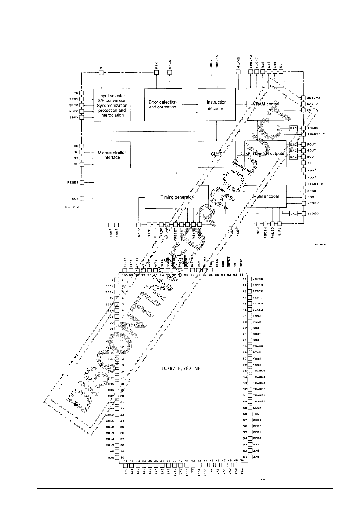
Block Diagram
Pin Assignment
No. 4861-2/19
LC7871E, 7871NE
Top view
Page 3
Specifications
Absolute Maximum Ratings at Ta = 25°C, VSS= 0 V
Allowable Operating Ranges at Ta = 25°C, V
SS
= 0 V
Electrical Characteristics at Ta = 25°C, V
SS
= 0 V, VDD= 5 V
No. 4861-3/19
LC7871E, 7871NE
Parameter Symbol Ratings Unit
Maximum supply voltage V
DD
max VSS– 0.3 to +7.0 V
Maximum input voltage V
IN
max VSS– 0.3 to VDD+ 0.3 V
Maximum output voltage V
OUT
max VSS– 0.3 to VDD+ 0.3 V
Allowable power dissipation Pd max 500 mW
Operating temperature Topr –30 to +85 °C
Storage temperature Tstg –40 + 125 °C
Parameter Symbol Conditions min typ max Unit
Supply voltage V
DD
VDD1, VDD2, VDD3 4.5 5.5 V
V
IH
(1) RESET 0.7 V
DD
V
DD
V
SFSY, PW, SBSY, MUTE, TEST, TEST1, TEST2,
V
IH
(2) SON, M1/M2, N/P1, N/P2, PALID, HRESET, VRESET, 2.2 V
DD
V
Input high level voltage
1DB0 to 3, 2DB0 to 3
V
IH
(3) CH0 to 15, DEN, CL, CE, DI 0.8 V
DD
V
DD
V
V
IH
(4) S 0.9 V
DD
V
DD
V
V
IL
(1) RESET V
SS
0.3 V
DD
V
SFSY, PW, SBSY, MUTE, TEST, TEST1, TEST2,
V
IL
(2) SON, M1/M2, N/P1, N/P2, PALID, HRESET, VRESET, V
SS
0.8 V
Input low level voltage
1DB0 to 3, 2DB0 to 3
VIL(3) CH0 to 15, DEN, CL, CE, DI V
SS
0.2 V
DD
V
V
IL
(4) S V
SS
0.1 V
DD
V
Input middle level voltage V
IM
S 0.37 V
DD
0.43 V
DD
V
Data setup time t
DS
DI, CL: Figure 1 200 ns
Data hold time t
DH
DI, CL: Figure 1 200 ns
High level clock pulse width t
WøH
CL: Figure 1 400 ns
Low level clock pulse width t
WøL
CL: Figure 1 400 ns
DO setup time t
DOS
DO, CL: Figure 1 250 450 ns
fin (1) XIN1 14.31818 MHz
fin (2) XIN2 17.734476 MHz
Input frequency 4FSC2
NTSC mode 14.31818 MHz
PAL mode 17.734476 MHz
FSCIN
NTSC mode 3.58 MHz
PAL mode 4.43 MHz
CE wait time t
CP
CE, CL: Figure 1 400 ns
CE setup time t
CS
CE, CL: Figure 1 0 ns
CE hold time t
CH
CE, CL: Figure 1 400 ns
Input amplitude V
IN
XIN1, XIN2, 4FSC2, FSCIN:
0.3 5 Vp-p
Sine wave, capacitive coupling
Reset pulse width t
WRES
RESET 400 ns
Parameter Symbol Conditions min typ max Unit
I
DD
(1) VDD12640mA
Current drain I
DD
(2) VDD22640mA
I
DD
(3) VDD31115mA
RESET, SFSY, PW, SBSY, CE, DI, CL, MUTE, TEST,
I
IH
(1) TEST1, TEST2, SON, M1/M2, N/P1, N/P2, VRESET, 5 µA
Input high level current
HRESET: V
IN
= V
DD
IIH(2) CH0 to 15, DEN: VIN= V
DD
30 100 200 µA
Continued on next page.
Page 4
Continued from preceding page.
No. 4861-4/19
LC7871E, 7871NE
Parameter Symbol Conditions min typ max Unit
RESET, SFSY, PW, SBSY, CE, DI, CL, MUTE, TEST,
IIL(1) TEST1, TEST2, SON, M1/M2, N/P1, N/P2, VRESET, –5µA
Input low level current
HRESET: V
IN
= V
SS
IIL(2) PALID: VIN= V
SS
–400 –200 –60 µA
SBCK, 1WE, RAS, 1A0 to 7, 2A0 to 7, CAS, OE, 2WE,
Output high level voltage V
OH
(1) CDGM, TRANS0 to 5, 2FSC, YS, CSYNC, VSYNC, VDD– 1V
DD
V
EFLG, FSX, FSC, 1DB0 to 3, 2DB0 to 3: I
O
= –0.5 mA
SBCK, 1WE, RAS, 1A0 to 7, 2A0 to 7, CAS, OE, 2WE,
V
OL
(1) CDGM, TRANS0 to 5, 2FSC, YS, CSYNC, VSYNC, V
SS
0.4 V
Output low level voltage
EFLG, FSX, FSC, 1DB0 to 3, 2DB0 to 3: I
O
= 2 mA
V
OL
(2) DO: IO= 5 mA V
SS
0.75 V
Output off leakage current I
OFF
DO, 1DB0 to 3, 2DB0 to 3 –5+5µA
Built-in feedback resistance RX XIN1, XIN2, 4FSC2, FSCIN 1 MΩ
6-bit D/A converter
V
REF
(1) ROUT, BOUT, GOUT, TRANS 3.95 4 4.05 V
reference voltage
6-bit D/A converter
R
DA
(1) ROUT, BOUT, GOUT, TRANS 150 Ω
output resistance
8-bit D/A converter
V
REF
(2) VIDEO 3.65 3.70 3.75 V
reference voltage
8-bit D/A converter
R
DA
(2) VIDEO 150 Ω
output resistance
8-bit D/A converter output level VDAC VIDEO: Figure 9
Random read/write cycle time t
RC
Figures 2 and 3 400 ns
Page mode cycle time t
PC
Figures 4 and 5 130 ns
RAS precharge time t
RP
Figures 2, 3, 4, 5 and 6 100 ns
RAS pulse width t
RAS
Figures 2, 3 and 6 120 ns
RAS pulse width (page mode) t
RASP
Figures 4 and 5 18000 ns
RAS hold time t
RSH
Figures 2, 3, 4 and 5 60 ns
CAS hold time t
CSH
Figures 2 and 3 120 ns
CAS pulse width t
CAS
Figures 2, 3, 4 and 5 60 ns
CAS precharge time t
CPN
Figure 6 50 ns
CAS precharge time (page mode) t
CP
Figures 4 and 5 50 ns
Row address setup time t
ASR
Figures 2, 3, 4 and 5 100 ns
Row address hold time t
RAH
Figures 2, 3, 4 and 5 50 ns
Column address setup time t
ASC
Figures 2, 3, 4 and 5 0 ns
Column address hold time t
CAH
Figures 2, 3, 4 and 5 50 ns
Read command setup time t
RCS
Figure 2 150 ns
Read command hold time
t
RCH
Figure 2 120 ns
(referenced to CAS)
Read command hold time
t
RRH
Figure 2 120 ns
(referenced to RAS)
Write command setup time t
WCS
Figure 3 100 ns
Write command hold time t
WCH
Figure 3 50 ns
Write command pulse width t
WP
Figure 3 150 ns
Write data setup time t
DS
Figure 3 100 ns
Write data hold time t
DH
Figure 3 100 ns
CAS setup time
t
CSR
Figure 6 50 ns
(CAS before RAS)
CAS hold time (CAS before RAS) t
CHR
Figure 6 50 ns
RAS precharge · CAS active time t
RPC
Figure 6 50 ns
Read data setup time t
RDS
Figures 2, 4 and 5 20 ns
Read data hold time t
RDH
Figures 2, 4 and 5 10 ns
VIDEO setup time t
VS
Superimposition: Figure 7 20 25 ns
SBCK output delay time t
SD
Figure 8
NTSC mode 4.749 5.029 µs
PAL mode 4.793 5.075 µs
SBCK cycle frequency f
SC
Figure 8
NTSC mode 223.7 kHz
PAL mode 221.7 kHz
PW setup time t
PWS
Figure 8 100 ns
Page 5
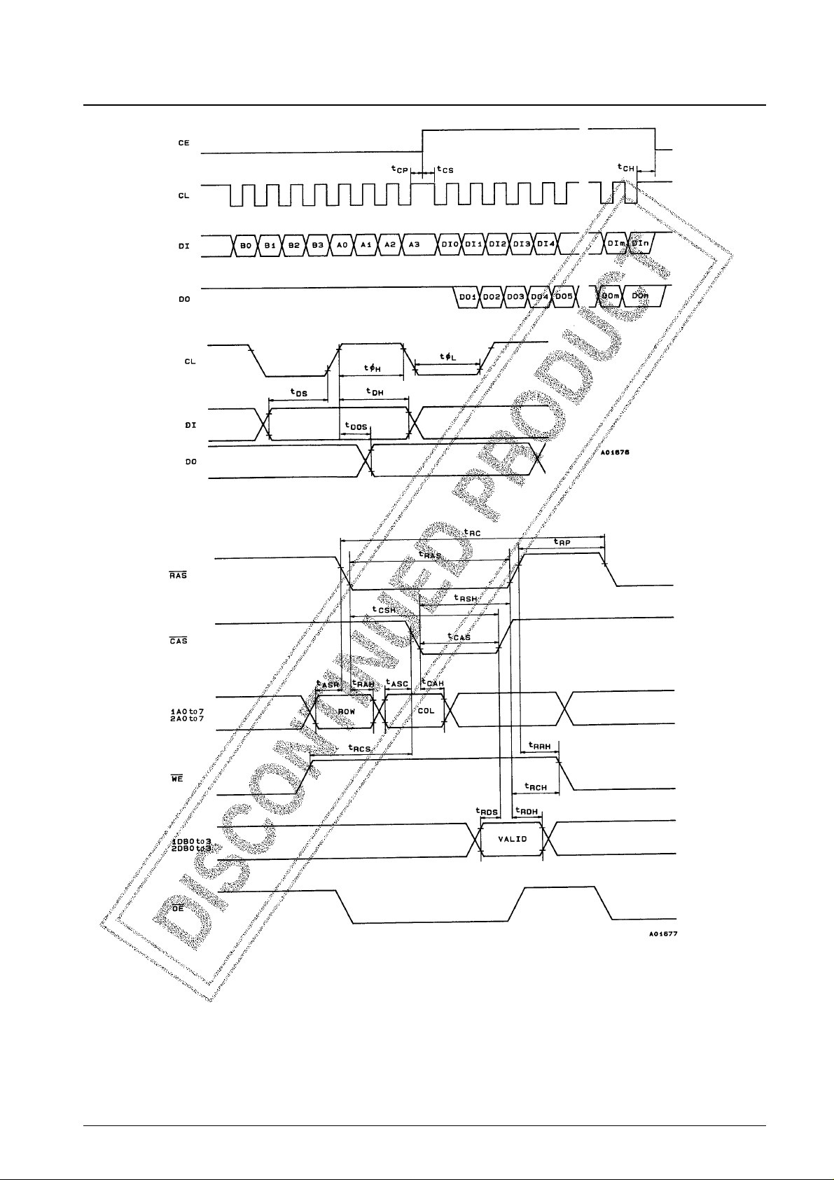
Figure 1 Microcontroller Interface Timing
Figure 2 DRAM Read Cycle
No. 4861-5/19
LC7871E, 7871NE
Page 6
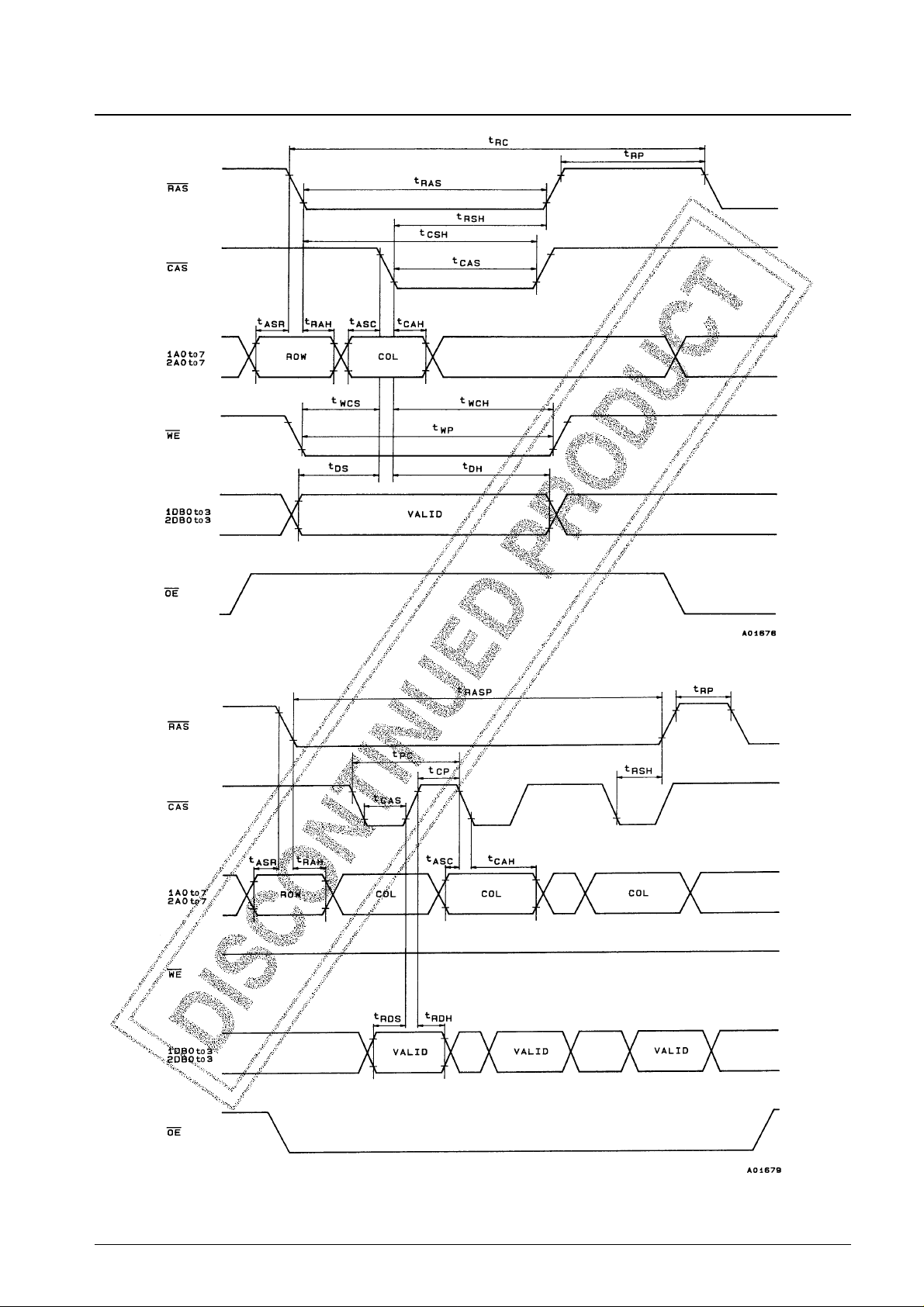
Figure 3 DRAM Early Write Cycle
Figure 4 DRAM Page Mode Read Cycle
No. 4861-6/19
LC7871E, 7871NE
Page 7

Figure 5 DRAM Page Mode Write Cycle
Figure 6 DRAM CAS before RAS Refresh Cycle
Figure 7 Phase Relationships in Superimposition Mode
No. 4861-7/19
LC7871E, 7871NE
Page 8

S pin low
Figure 8 Subcode Interface
Figure 9 Composite Video Signal Output (8 bits)
No. 4861-8/19
LC7871E, 7871NE
Page 9

Pin Functions
No. 4861-9/19
LC7871E, 7871NE
Pin No. Pin I/O Function
1 S I CD DSP selection: High level input: LC7861N/67, middle level input: LC7860K/63, low level input: LC7868/69
2 SBCK O P to W subcode read clock
3 SFSY I Subcode frame synchronization signal
4 PW I P to W subcode data
5 SBSY I Subcode block synchronization signal
6V
DD
1 — Digital system power supply
7 CE I Control during serial input or serial output
8 DO O Serial data output
9 DI I Serial data input
10 CL I Serial data I/O clock
11 MUTE I Control signal used to specify that the subcode data be handled as invalid
12 V
SS
1 — Digital system ground
13 CH0 I
14 CH1 I
15 CH2 I
16 CH3 I
17 CH4 I
18 CH5 I
19 CH6 I
20 CH7 I
Channel selection pins. A high level enables the corresponding channel.
21 CH8 I
These pins have built-in pull-down resistors.
22 CH9 I
23 CH10 I
24 CH11 I
25 CH12 I
26 CH13 I
27 CH14 I
28 CH15 I
29 1WE O Primary DRAM control
30 RAS O Control pin shared by primary and secondary DRAM
31 1A0 O
32 1A1 O
33 1A2 O
34 1A3 O
Primary DRAM address
35 1A4 O
36 1A5 O
37 1A6 O
38 1A7 O
39 1DB0 I/O Primary DRAM data
40 CAS O Control pin shared by primary and secondary DRAM
41 1DB1 I/O Primary DRAM data
42 OE O Control pin shared by primary and secondary DRAM
43 1DB2 I/O
Primary DRAM data
44 1DB3 I/O
45 2WE O Secondary DRAM control
46 2A0 O
47 2A1 O
48 2A2 O
49 2A3 O
Secondary DRAM address
50 2A4 O
51 2A5 O
52 2A6 O
53 2A7 O
Continued on next page.
Page 10

Continued from preceding page.
No. 4861-10/19
LC7871E, 7871NE
Pin No. Pin I/O Function
54 2DB0 I/O
55 2DB1 I/O
Secondary DRAM data
56 2DB2 I/O
57 2DB3 I/O
58 TEST I IC testing
59 CDGM O Outputs a high level when reading a CD-G disk
60 TRANS0 O
61 TRANS1 O
62 TRANS2 O
Transparency digital output
63 TRANS3 O
64 TRANS4 O
65 TRANS5 O
66 V
SS
2 — Analog system ground
67 V
DD
2 — Analog system power supply
68 BIAS1 O Ripple rejection capacitor connection
69 TRANS O Define-transparency 6-bit D/A converter output
70 ROUT O Red data 6-bit D/A converter output
71 GOUT O Green data 6-bit D/A converter output
72 BOUT O Blue data 6-bit D/A converter output
73 V
SS
3 — Analog system ground
74 V
DD
3 — Analog system power supply
75 BIAS2 O Ripple rejection capacitor connection
76 VIDEO O Composite video output (8-bit D/A converter output)
77 TEST1 I
IC testing
78 TEST2 I
79 FSCIN I Subcarrier clock input (feedback resistor built in)
80 VSYNC O Vertical synchronization signal output
81 2FSC O 2FSC output
82 YS O Superimposition control output
83 CSYNC O Composite sync output
84 SON I Superimposition on/off
85 EFLG O Error state monitor
86 FSX O Error state monitor trigger
87 M1/M2 I Selects one or two 256 kbit DRAMs: High: one DRAM, low: two DRAMs
88 DEN I Disk information display enable: High: BGC, low: enable (pull-down resistor built in)
89 PALID I PAL mode superimposition control (pull-up resistor built in)
90 HRESET I External horizontal timing control
91 FSC O Subcarrier clock output NTSC mode: 3.579545 MHz, PAL mode: 4.433619 MHz
92 VRESET I External vertical timing control
93 4FSC2 I External superimposition mode clock input (feedback resistor built in)
94 RESET I Reset input
95 N/P1 I NTSC/PAL selection: High: NTSC, low: PAL (RGB encoder)
96 N/P2 I NTSC/PAL selection: High: NTSC, low: PAL (CD-G decoder)
97 XIN2 I
Crystal oscillator connection 17.734476 MHz (PAL)
98 XOUT2 O
99 XIN1 I
Crystal oscillator connection 14.31818 MHz (NTSC)
100 XOUT1 O
Page 11

CD-EG Instructions
Of the instructions in the R to W subcode described in the CD Red Book, the LC7871E and the LC7871NE support the
following:
1. MODE = 0, ITEM = 0: ZERO mode
2. MODE = 1, ITEM = 0: LINE GRAPHICS mode
• Write FONT instruction (4)
• Write Scroll SCREEN instruction (12)
3. MODE = 1, ITEM = 1: TV-GRAPHICS mode
• Preset MEMORY instruction (1)
• Preset BORDER instruction (2)
• Write FONT FOREGROUND/BACKGROUND instruction (6)
• Scroll SCREEN with preset instruction (20)
• Scroll SCREEN with Copy instruction (24)
• Load CLUT color-0...7 instruction (30)
• Load CLUT color-8...15 instruction (31)
• EXCLUSIVE-OR FONT instruction (38)
• Define color Transparency instruction (28)
4. MODE = 1, ITEM = 1 & 2: EXTENDED TV-GRAPHICS mode
• MEMORY Control instruction (3)
• Write additional FONT FOREGROUND/BACKGROUND instruction (6)
• EXCLUSIVE-OR additional FONT with 2 colors instruction (14)
• Load CLUT color instruction (16-47)
• Load CLUT additional color instruction (48-63)
Pin Applications
1. Crystal Clock Oscillator: Pins XIN1, XOUT1, XIN2, XOUT2, N/P1, N/P2, FSC, CSYNC, 2FSC and VSYNC
The XIN1 and XOUT1 pins are for use with a 14.31818 MHz (NTSC) crystal oscillator. The XIN2 and XOUT2 pins
are for use with a 17.734476 MHz (PAL) crystal oscillator. The LC7871E and LC7871NE provide the above two
crystal oscillator systems. Depending on the application, either a single crystal can be connected, or alternatively two
crystals can be used allowing control from both the N/P1 and the N/P2 pins. The N/P1 pin switches the RGB encoder
block between PAL and NTSC and the N/P2 pin switches the CD-G decoder block between PAL and NTSC. The
FSC and 2FSC pins output the crystal oscillator frequency divided by 4 and 2 (2/5 in PAL mode) respectively. The
CSYNC pin outputs a composite sync signal, and the VSYNC pin outputs a vertical sync signal.
The table below shows the pin outputs in the various modes.
No. 4861-11/19
LC7871E, 7871NE
XIN1, XOUT1 XIN2, XOUT2 N/P1 N/P2 TV Standard FSC 2FSC CSYNC
14.31818 MHz * H H NTSC/M 3.579545 MHz 7.15909 MHz 16.65155767 ms
* 17.734476 MHz L L PAL/GBIDH 4.433619 MHz 7.093790 MHz 20.09588555 ms
14.30244 MHz * L H PAL/M 3.575611 MHz 7.15122 MHz 16.6698829 ms
Page 12

Recommended Crystal Oscillator Constants
2. Subcode Interface: Pins S, SBSY, SFSY, PW, SBCK and MUTE
The S pin selects one of three interface modes, as shown in the table below. When a high level is applied to the
MUTE pin, SBSY and PW input are disabled, and SBCK output is disabled.
Note that the “M” level is typically 0.4 V
DD
.
• LC7860 interface (Symbols in parentheses are LC7860 pins.)
The conditions for SBCK output are as follows: confirmation of low levels on the SFSY pin about 2.2 µs after a
falling edge on SFSY.
Note: * SFSY will be high during the S0 and S1 periods.
* The SBSY pin must be held low.
• LC7861N/67 interface (Symbols in parentheses are DSP pins.)
The conditions for SBCK output are as follows: confirmation of a low level on the SBSY pin about 2.2 µs after a
falling edge on the SFSY pin in the LC7871E.
In the LC7871NE the conditions are confirmation of a low level on the SBSY pin about 2.2 µs after a rising edge
on the SFSY pin.
No. 4861-12/19
LC7871E, 7871NE
SH M L
Mode LC7861N/67 interface LC7860K/63 interface LC7868/69 interface
Manufacturer Oscillator Cin/Cout
NTSC CITIZEN WATCH CO., LTD CSA-309 (14.31818 MHZ) 5 to 8 pF (Cin = Cout)
PAL CITIZEN WATCH CO., LTD CSA-309 (17.734475 MHZ) 5 to 12 pF (Cin = Cout)
Page 13

• LC7868/69 interface
This interface is identical to that described in item 2 above, except that the SBCK polarity is reversed, i.e., the shift
occurs on a rising edge.
3. DRAM Interface: Pins 1A0 to 1A7, 1DB0 to 1DB3, RAS, CAS, 1WE, OE, 2A0 to 2A7, 2DB0 to 2DB3, 2WE and
M1/M2
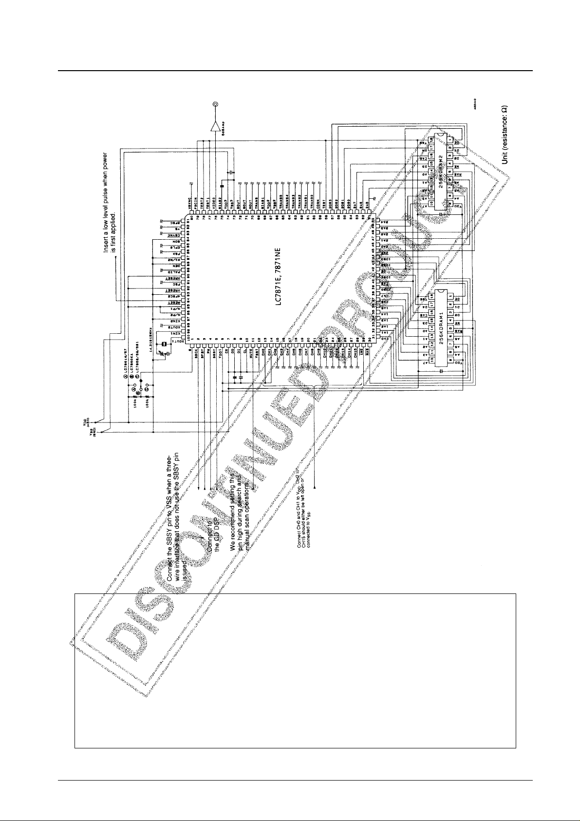
The LC7871E and LC7871NE use external 64k by 4-bit DRAMs.
Two external DRAMs are required for CD-EG. Only one external DRAM is required for CD-G. The M1/M2 pin
setting must match the number of DRAMs actually used. When single memory chip operation is selected by setting
the M1/M2 pin high, the pins 2DB0 to 3 function in output mode. Thus the pins 2A0 to 7, 2DB0 to 3, 2WE and 2OE
can be left open.
4. Display Format: Pins DEN, N/P1, N/P2, CSYNC, VRESET, HRESET, YS, VIDEO, PALID, TRANS and TRANS0
to TRANS5
• Data which has undergone error detection and correction is encoded by the built-in RGB encoder, converted to
analog by the 8-bit D/A converter, and output from the VIDEO pin. This system can handle both PAL and NTSC
modes, and either mode can be specified from the N/P pin. See item 1 for the states of the pins in the PAL and
NTSC modes.
• The YS, VRESET, HRESET, PALID, TRANS and TRANS0 to TRANS5 pins are used in superimposition
processing.
• The DEN pin is a display control pin. When this pin is at a low level, the internal font data is output, and when at a
high level, the color data loaded into the registers is output. The default state is blue.
No. 4861-13/19
LC7871E, 7871NE
Page 14

5. Channel Selection: Pins CH0 to CH15
The channel can be selected by controlling the values of the CH0 to CH15 pin input values. The logical OR is taken
with the microprocessor input register.
6. CD Graphics Monitor: The CDGM pin
The CDGM signal goes high when the LC7871E or LC7871NE receives, even once, any one of the page 11 CDG
instructions. Since the circuits are connected as soon as this signal goes high in the power on state, a reset will be
required when changing disks if this pin is used.
7. Video Output: The VIDEO pin
A composite video signal can be acquired from the VIDEO pin. The output level from the 8-bit D/A converter is
1.25 Vp-p. Therefore, an external 6 dB video amplifier is required to acquire a 1 Vp-p rated output.
8. Error Flag Output: Pin EFLG and FSX
The error detection result can be monitored from the EFLG pin.
Microcontroller Interface (CCB bus)
1. 2N byte command input
Address (F4h): lsb [00101111] msb
Control item: lsb [0---AAAA] msb A = register number
Register 0 (mode setting)
Data: lsb [ABCDEFGH] msb. The default is[00000110].
A = VRAM/BG 0: Display the contents of VRAM
1: Display the background color
B = TV/LINE 0: TV mode (Extended TV mode)
1: Line graphics mode
C = Disk command enable
0: Disk commands are accepted. MGC commands (microcontroller graphics commands,
executed by 19-byte command inputs) are executed between disk commands,
1: Disk commands are ignored and only MGC commands are executed.
No. 4861-14/19
LC7871E, 7871NE
Page 15

D = Command select
0: Normal operation
1: Register 9 is used for VRAM display control (PM or SM) and MGC access memory
control.
EFG = Comparison conditions for superimposition mode (only valid when SON = 1)
EF = 00: No comparison performed.
01: When the border color is not black, YS is set high (display) for portions that do not
match the border color, and is set low (clear) otherwise.
11: YS is set high for sections that do not match the chroma key color, and is set low
otherwise.
G = 0: When EF is 00 or the comparison condition is false for EF = 01, the whole screen is set
low (clear).
G = 1: When EF is 00 or the comparison condition is false for EF = 01, the whole screen is set
high (display).
H = INIT 0: Normal operation
1: Internal reset
On an internal reset the display screen is reset to the BGC screen.
Register 1 (screen position adjustment)
Data: lsb [HHHHVVVV] msb. The default is [00000000].
H = Horizontal direction. Specified as a two’s complement value with positive values indicating a shift to the
left. The position can be shifted from –16 to +14 dots from the center in two dot increments.
V = Vertical direction. Specified as a two's complement value with positive values indicating an upwards shift.
The position can be shifted from –16 to +14 dots from the center in two dot increments.
Register 2 (on/off control of channels 0 through 7)
Data: lsb [CCCCCCCC] msb. The default is [00000000].
C = CH0 to CH7. 0: off, 1: on
Channels 0 through 7 are controlled according to the logical OR of this register and the CH0 to CH7 input pins.
Register 3 (on/off control of channels 8 through 15)
Data: lsb [CCCCCCCC] msb. The default is [00000000].
C = CH8 to CH15. 0: off, 1: on
Channels 8 through 15 are controlled according to the logical OR of this register and the CH8 to CH15 input
pins.
Register 4 (BGC R and G setting)
Data: lsb [RRRRGGGG] msb. The default is [00000000].
Register 5 (BGC B setting)
Data: lsb [----BBBB] msb. The default is [----0101].
Register 6 (chroma key color setting, R)
Data: lsb [--RRRRRR] msb. The default is [--010000].
Register 7 (chroma key color setting, G)
Data: lsb [--GGGGGG] msb. The default is [--010000].
Register 8 (chroma key color setting, B)
Data: lsb [--BBBBBB] msb. The default is [--010000].
No. 4861-15/19
LC7871E, 7871NE
Page 16

Register 9 (VRAM display and control switching)
Data: lsb [----DDWW] msb. The default is [----1001].
This register switches the display between the two VRAMs (primary memory and secondary memory) and also
sets the MGC access. (Disk command access is limited to PM access.) Note that these settings are only valid
when the register 0 command selection is set to 1 and VRAM is 512 kbytes. (The item 2 command will be
ignored and 16-color display used.)
DD = Display memory control (01: display PM, 10: display SM, 11: additive mix)
WW = MGC access memory control (01: work PM, 10: work SM, 11: work PM & SM)
Register 10 (Software reset, external sync on/off, test mode)
Data: lsb [TTT--YSR] msb. The default is [000--000].
T = Test mode setting
R = Software reset, 0: Normal operation, 1: Reset
The display screen will be held until the next command is executed when a software reset is
performed.
S = 0: TRANS is initialized on a software reset.
1: TRANS is not initialized on a software reset.
Y = 0: Reset on HRESET and VRESET in external clock mode (SON = 1).
1: Reset on VRESET in external clock mode (SON = 1). (HRESET is unnecessary.)
Register 11 (subtitle vertical scrolling)
Data: lsb [---VVVVV] msb. The default is [---00000].
The screen position can be scrolled vertically in units of the font height.
V = Vertical scroll distance (0 to 17 font heights.)
Register 12 (subtitle horizontal scrolling)
Data: lsb [--HHHHHH] msb. The default is [--000000].
The screen position can be scrolled horizontally in units of the font width.
H = Horizontal scroll distance (0 to 49 font widths.)
Register 13 (TRANS setting, only valid when SON = 1)
Data: lsb [PSBBBBBB] msb. The default is [11000000].
P = 1: Makes the PM TRANS setting valid. 0: Invalid (whole screen display)
S = 1: Makes the SM TRANS setting valid. 0: Invalid (whole screen display)
B = The BGC TRANS value
Register 14 (YS and TRANS output timing)
Data: lsb [----TTTT] msb. The default value is [----0001].
T = The phase between the video signal and the YS and TRANS (digital output) signals in 70 ns units.
The value of T can be set to one of the ten values in the range 0 to 9. In NTSC mode, YS and TRANS will be
in phase with the RGB output when T = 0, and with the C output when T = 8 or 9.
2. 19-byte command input (MGC write)
Address (F4h): lsb [00101111] msb
Control item: lsb [1-------] msb
Data: lsb [--WVUTSR] msb. W to R are the subcode inputs.
Executed on the falling edge of the CE signal. Note that this operation cannot be executed during command
execution or when TIMER is 10 or 11.
No. 4861-16/19
LC7871E, 7871NE
Page 17

3. Single-byte command output (internal status readout)
Address (F5h): lsb [10101111] msb
Control item: lsb [0-------] msb
Data: lsb [-ABCTTTT] msb
A = Read request bit. 1: The packed data has been updated. Read access will be possible within 1.1 ms has
passed.
0: Packed data read out prohibited state.
B = Command execution in progress.
1: Command execution in progress.
0: Command wait state.
C = VBLANK. Set to 1 during the vertical blanking period.
T = Timer. Outputs the command cycle (3.30 ms) from the CD divided by 12.
T = 0: 0.00 ms
1: 0.27 ms
2: 0.55 ms
:
10: 2.75 ms
11: 3.02 ms (command issued from the CD)
0: 3.30 ms (0.00 ms)
When the register 0 C value is 0, MGC must be written in the interval when the timer
is between 0 and 9 in the command wait state.
4. 19-byte command output (packed data readout)
No. 4861-17/19
LC7871E, 7871NE
Page 18

Address (F5h): lsb [10101111] msb
Control item: lsb [1-------] msb
Check flag: lsb [-ABCQQPP] msb
Data: lsb [--WVUTSR] msb
A is set to 1 when the following 18 bytes are guaranteed and furthermore, this is the first time that the data has
been read out. (The readout must be completed within 1.1 ms.)
B, C: Disk identification flags
BC = 00: CD
BC = 10: CD-G
BC = 11: CD-EG
Q = QF0 and QF1 (error correction Q flags)
P = PF0 and PF1 (error correction P flags)
Note that when it is not necessary to read out all 19 bytes, the read can be discontinued at any time in byte units.
Note that it is also possible to read out only the check flag.
No. 4861-18/19
LC7871E, 7871NE
Page 19
PS No. 4861-19/19
LC7871E, 7871NE
LC7871E and LC7871NE CD-EG Application Circuit (NTSC)
This catalog provide information as of May, 1995. Specifications and information herein are subject to change
without notice.
■ No products described or contained herein are intended for use in surgical implants, life-support systems, aerospace
equipment, nuclear power control systems, vehicles, disaster/crime-prevention equipment and the like, the failure of
which may directly or indirectly cause injury, death or property loss.
■ Anyone purchasing any products described or contained herein for an above-mentioned use shall:
➀ Accept full responsibility and indemnify and defend SANYO ELECTRIC CO., LTD., its affiliates, subsidiaries and
distributors and all their officers and employees, jointly and severally, against any and all claims and litigation and all
damages, cost and expenses associated with such use:
➁ Not impose any responsibility for any fault or negligence which may be cited in any such claim or litigation on
SANYO ELECTRIC CO., LTD., its affiliates, subsidiaries and distributors or any of their officers and employees
jointly or severally.
■ Information (including circuit diagrams and circuit parameters) herein is for example only; it is not guaranteed for
volume production. SANYO believes information herein is accurate and reliable, but no guarantees are made or implied
regarding its use or any infringements of intellectual property rights or other rights of third parties.
 Loading...