

Overview
The LC78711E is a CMOS LSI that provides graphics
display drawing functions. In addition to implementing
graphics display for NTSC and PAL signals, it provides
two 32 × 32-dot sprite display patterns and can easily
implement a wide range of displays.
Features
• Two-chip structure consisting of this LSI, the
LC78711E, and an external 64-K × 4-bit RAM. (An
RGB encoder is built in.)
• Graphics drawing controlled by a microprocessor over a
serial interface.
• Includes two crystal oscillator systems, one for NTSC
and one for PAL, and these system can be easily
switched using the provided control pin.
The standard clocks and all necessary internal timings
can be generated by connecting two crystals, a
14.31818-MHz crystal for NTSC, and a 17.734476-MHz
crystal for PAL.
• Two 32 × 32-dot sprite patterns provided. Up to two
sprites can be displayed, either two different types or the
same pattern in two different locations.
• 16 colors from a palette of 4096 colors can be displayed
in graphics screens, and seven colors can be displayed in
sprite patterns.
• Y/C signal outputs (two 8-bit D/A converter outputs)
• Supports the superimpose function, and provides a
timing signal output.
• Provides a color bar signal output function.
• Adopts an 8-bit serial data input format for the external
control input.
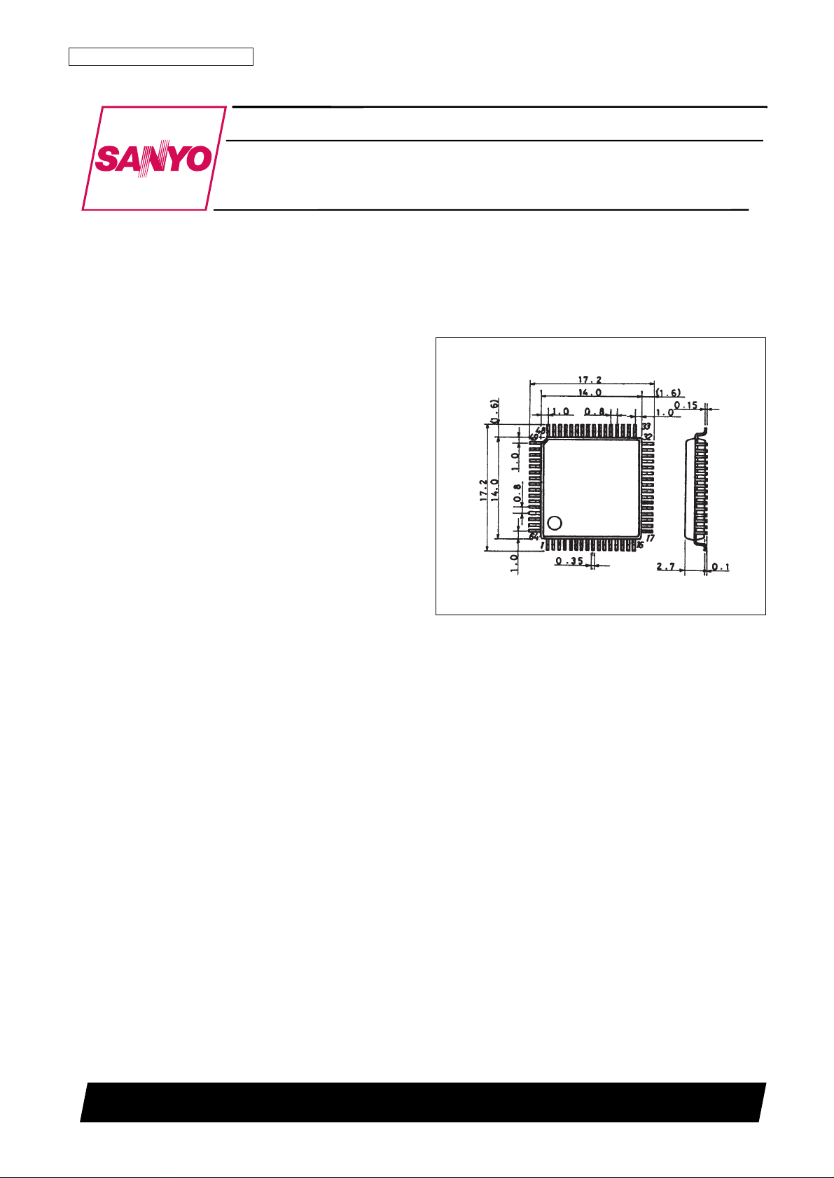
Package Dimensions
unit: mm
3159-QFP64E
CMOS LSI
63096HA (OT) No. 5476-1/43
SANYO: QFP64E
[LC78711E]
SANYO Electric Co.,Ltd. Semiconductor Bussiness Headquarters
TOKYO OFFICE Tokyo Bldg., 1-10, 1 Chome, Ueno, Taito-ku, TOKYO, 110 JAPAN
Graphics Display Processor
LC78711E
Ordering number : EN5476
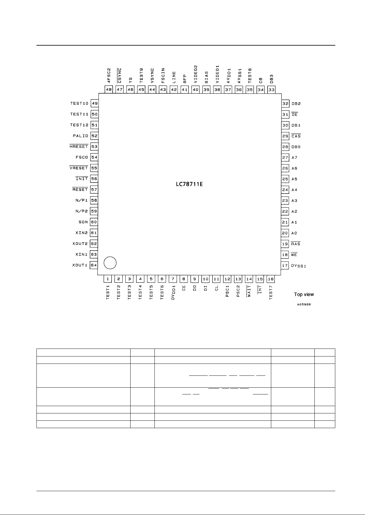
Pin Assignment
No. 5476-2/43
LC78711E
Parameter Symbol Conditions Ratings Unit
Maximum supply voltage V
DD
max AVDD1, DVDD1 VSS– 0.3 to VSS+ 7.0 V
TEST1, TEST2, TEST4, TEST5, TEST6, CE, DI, CL,
Maximum input voltage V
IN
max
TEST7, DB0 to DB3, CB, LINE, FSCIN, TEST9, 4FSC2,
VSS– 0.3 to VDD+ 0.3 V
TEST12, PALID, HRESET, VRESET, INIT, RESET, N/P1,
N/P2, SON, XIN1, XIN2
TEST3, DO, PSC1, PSC2, WAIT, INT, WE, RAS, A0 to A7,
Maximum output voltage V
OUT
max DB0 to DB3, CAS, OE, TEST8, BFP, VSYNC, YS, CSYNC, VSS– 0.3 to VDD+ 0.3 V
TEST10, TEST11, FSC0, XOUT1, XOUT2
Allowable power dissipation Pd max Ta = 25°C 500 mW
Operating temperature Topr –30 to +85 °C
Storage temperature Tstg –40 to +125 °C
Specifications
Absolute Maximum Ratings
No. 5476-3/43
LC78711E
Parameter Symbol Conditions
Ratings
Unit
min typ max
Supply voltage V
DD
AVDD1, DVDD1 4.5 5.0 5.5 V
TEST1, TEST2, TEST4, TEST5, TEST6, CE, DI, TEST7,
VIH1 CB, LINE, TEST9, TEST12, PALID, HRESET, VRESET, 0.7 VDD1 VDD1 + 0.3 V
Input high-level voltage
N/P1, N/P2, SON
V
IH
2 CL, INIT, RESET 0.8 VDD1 VDD1 + 0.3 V
V
IH
3 DB0 to DB3 2.2 VDD1 + 0.3 V
TEST1, TEST2, TEST4, TEST5, TEST6, CE, DI, TEST7,
VIL1 CB, LINE, TEST9, TEST12, PALID, HRESET, VRESET, VSS1 – 0.3 0.3 VDD1 V
Input low-level voltage
N/P1, N/P2, SON
V
IL
2 CL, INIT, RESET VSS1 – 0.3 0.2 VDD1 V
V
IL
3 DB0 to DB3 VSS1 – 0.3 0.8 V
F
SCIN
1 XIN1 14.31818 MHz
F
SCIN
2 XIN2 17.73447 MHz
Input frequency F
SCIN
3
4FSC2: NTSC mode 14.31818 MHz
4FSC2: PAL mode 17.73447 MHz
F
SCIN
4
FSCIN: NTSC mode 3.57954 MHz
FSCIN: PAL mode 4.43361 MHz
Input amplitude
V
IN
1 FSCIN, 4FCS2 0.5 VDD1 Vp-p
V
IN
2 XIN1, XIN2 0.5 VDD1 Vp-p
Allowable Operating Ranges at Ta = –30 to +85°C, VSS= 0 V
Parameter Symbol Conditions
Ratings
Unit
min typ max
TEST1, TEST2, TEST4, TEST5, TEST6, CE, DI, CL,
Input high-level current
I
IH
1 TEST7, DB0 to DB3, LINE, PALID, HRESET, VRESET, 5 µA
INIT, RESET, N/P1, N/P2, SON: V
IN
= DVDD1
I
IH
2 CB, TEST9, TEST12: VIN= DVDD1 30 100 200 µA
TEST1, TEST2, TEST4, TEST5, TEST6, CE, DI, CL,
I
IL
1
TEST7, DB0 to DB3, CB, LINE, TEST9, TEST12,
–5 µA
Input low-level current
HRESET, VRESET, INIT, RESET, N/P1, N/P2, SON:
V
IN
= DVSS1
I
IL
2 PALID: VIN= DVSS1 –200 –100 –30 µA
TEST3, DO, PSC1, PSC2, WAIT, INT, BFP, WE, RAS,
Output high-level voltage V
OH
A0 to A7, CAS, OE, DB0 to DB3, TEST8, VSYNC, YS, VDD1 – 1 VDD1 V
CSYNC, TEST10, TEST11, FSCO: I
OH
= –0.5 mA
TEST3, DO, PSC1, PSC2, WAIT, INT, BFP, WE, RAS,
Output low-level voltage V
OL
A0 to A7, CAS, OE, DB0 to DB3, TEST8, VSYNC, YS, V
SS
0.4 V
CSYNC, TEST10, TEST11, FSCO: I
OL
= 2.0 mA
Output off leakage current I
OFF
DB0 to DB3 –5 +5 µA
Internal feedback resistance R
X
XIN1, XIN2, FSCIN, 4FSC2 1 MΩ
Clock duty fduty FSCIN, 4FSC2 40 60 %
8-bit D/A converter reference
V
REF
VIDEO1, VIDEO2 2.30 2.50 V
voltage
8-bit D/A converter output
R
DA
VIDEO1, VIDEO2 300 Ω
resistance
Operating current drain
I
DD
1 AVDD1 26 40 mA
I
DD
2 DVDD1 26 40 mA
Electrical Characteristics at Ta = –30 to +85°C, DVDD1 = AVDD1 = 5 V unless otherwise specified.
No. 5476-4/43
LC78711E
Parameter Symbol Conditions
Ratings
Unit
min typ max
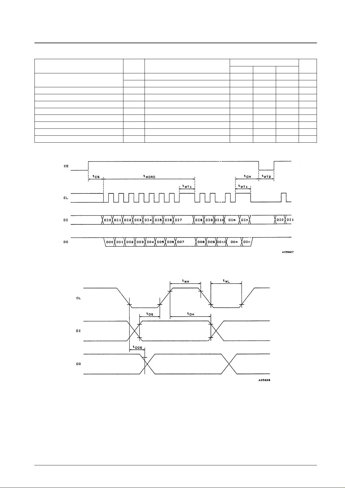
Minimum input pulse width
t
WH
CL, high-level pulse width 75 ns
t
WL
CL, low-level pulse width 75 ns
Data setup time t
DS
DI, CL 20 ns
Data hold time t
DH
DI, CL 20 ns
CE setup time t
CS
CE, CL 0 ns
CE hold time t
CH
CE, CL 300 ns
DO setup time t
DOS
DO, CL 30 ns
Data acquisition time t
WT
1 Serial data acquisition time 150 ns
Data restart time t
WT
2 Serial data restart time 1.0 µs
Single word write time t
WORD
DI, CL (1 word = 8 bits) 1.35 µs
Electrical Characteristics at Ta = 25°C, VDD= 5.0 V, Fscp = 15.625 kHz
No. 5476-5/43
LC78711E
Basic Specifications
Pin no. Pin Pin type I/O Polarity Pin function
1 TEST1 Test input I Positive Test input. Must be connected to ground during normal operation.
2 TEST2 Test input I Positive Test input. Must be connected to ground during normal operation.
3 TEST3 Test output O Positive Test output
4 TEST4 Test input I Positive Test input. Must be connected to ground during normal operation.
5 TEST5 Test input I Positive Test input. Must be connected to ground during normal operation.
6 TEST6 Test input I Positive Test input. Must be connected to ground during normal operation.
7 DV
DD
1 Power supply (+5 V) — — Digital system power supply
8 CE Enable input I Positive Serial I/O data control input
9 DO Data output O Positive Serial data output
10 DI Data input I Positive Serial data input
11 CL Clock input I Positive Serial data I/O clock input
12 PSC1 Monitor 1 output O Positive Serial input monitor signal output
13 PSC2 Monitor 2 output O Positive Command monitor signal output
14 WAIT Wait signal output O Negative Serial input wait signal output (for use with bit maps)
15 INT Wait signal output O Negative Serial input wait signal output (for use with the sprite function)
16 TEST7 Test input I Positive Test input. Must be connected to ground during normal operation.
17 DV
SS
1 Ground — — Digital system ground
18 WE DRAM output O Negative DRAM write enable signal output
19 RAS DRAM output O Negative DRAM row address strobe signal output
20 A0 DRAM output I/O Positive DRAM address (A0) output (Functions as an input in test mode.)
21 A1 DRAM output I/O Positive DRAM address (A1) output (Functions as an input in test mode.)
22 A2 DRAM output I/O Positive DRAM address (A2) output (Functions as an input in test mode.)
23 A3 DRAM output I/O Positive DRAM address (A3) output (Functions as an input in test mode.)
24 A4 DRAM output I/O Positive DRAM address (A4) output (Functions as an input in test mode.)
25 A5 DRAM output I/O Positive DRAM address (A5) output (Functions as an input in test mode.)
26 A6 DRAM output I/O Positive DRAM address (A6) output (Functions as an input in test mode.)
27 A7 DRAM output I/O Positive DRAM address (A7) output (Functions as an input in test mode.)
28 DB0 DRAM input and output I/O Positive DRAM data (D0) input and output
29 CAS DRAM output O Negative DRAM column address strobe signal output
30 DB1 DRAM input and output I/O Positive DRAM data (D1) input and output
31 OE DRAM output O Negative DRAM read enable signal output
32 DB2 DRAM input and output I/O Positive DRAM data (D2) input and output
33 DB3 DRAM input and output I/O Positive DRAM data (D3) input and output
34 CB Color bar selection I Positive
Low: normal mode, high: color bar output
(A pull-down resistor is built in.)
35 TEST8 Test output O Positive Test output
36 AV
SS
1 Ground — — Analog system ground
37 AV
DD
1 Power supply (+5 V) — — Analog system power supply
38 VIDEO1 Video signal (Y) output O — Video (luminance) signal (analog) output (D/A converter output)
39 BIAS Capacitor connection O — Connections for a ripple exclusion capacitor
40 VIDEO2 Video signal (C) output O — Video (chrominance) signal (analog) output (D/A converter output)
41 BFP Burst flag signal output O Positive Burst signal output timing flag output
Line count selection
42 LINE Line count selection I — NTSC mode - Low: 263H, high: 262H
PAL mode - Low: 314H, high: 312H
43 FSCIN Clock input I Positive Superimpose subcarrier clock input (A feedback resistor is built in.)
44 VSYNC Vertical synchronization output O Negative Vertical synchronizing signal output
45 TEST9 Test input I Positive
Test input. Must be connected to ground during normal operation.
(A pull-down resistor is built in.)
46 YS Superimpose output O Negative Superimpose control output
47 CSYNC Composite synchronization output O Negative Composite synchronizing signal output
48 4FSC2 Clock input I Positive
External clock input for the superimpose function
(A feedback resistor is built in.)
49 TEST10 Test output O Positive Test output
50 TEST11 Test output O Positive Test output
Continued on next page.
No. 5476-6/43
LC78711E
Continued from preceding page.
Pin no. Pin Pin type I/O Polarity Pin function
51 TEST12 Test input I Positive Test input. Must be connected to ground during normal operation.
52 PALID PAL mode external control input I Positive
External superimpose function control input for PAL mode
(A pull-up resistor is built in.)
53 HRESET
External horizontal
I Negative External horizontal synchronization timing control input
synchronization input
Subcarrier clock output
54 FSCO Clock output O Positive NTSC mode: 3.579545 MHz
PAL mode: 4.433619 MHz
55 VRESET
External vertical
I Negative External vertical synchronization timing control input
synchronization input
56 INIT Initialization input I Negative System initialization signal input
57 RESET Reset input I Negative System reset signal input
58 N/P1 NTSC/PAL selection I Positive
NTSC/PAL selection input (RGB encoder block)
High: NTSC, low: PAL
59 N/P2 NTSC/PAL selection I Positive
NTSC/PAL selection input (decoder block)
High: NTSC, low: PAL
60 SON Superimpose control I Positive
Superimpose function on/off control input
High: superimpose on
61 XIN2
Crystal oscillator element
I —
Connections for the PAL crystal oscillator element
62 XOUT2
connections
O —
(4·fsc = 17.734476 MHz)
63 XIN1
Crystal oscillator element
I —
Connections for the NTSC crystal oscillator element
64 XOUT1
connections
O —
(4·fsc = 14.31818 MHz)
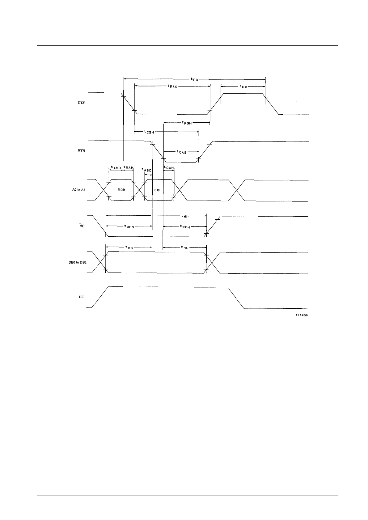
Parameter Symbol Conditions
Ratings
Unit
min typ max
Random read/write cycle t
RC
250 ns
Page mode cycle t
PC
130 ns
RAS access time t
RAC
210 ns
CAS access time t
CAC
10 ns
Output turn off delay t
OFF
20 ns
RAS precharge time t
RP
100 ns
RAS pulse width t
RAS
120 ns
RAS pulse width (page mode) t
RASP
18000 ns
RAS hold time t
RSH
60 ns
CAS hold time t
CSH
120 ns
CAS pulse width t
CAS
60 ns
CAS precharge time t
CPN
50 ns
CAS precharge time t
CP
Page mode 50 ns
Row address setup time t
ASR
100 ns
Row address hold time t
RAH
50 ns
Column address setup time t
ASC
0 ns
Column address hold time t
CAH
50 ns
Read command setup time t
RCS
150 ns
Read command hold time t
RCH
Referenced to CAS 120 ns
Read command hold time t
RRH
Referenced to RAS 120 ns
Write command setup time t
WCS
100 ns
Write command hold time t
WCH
50 ns
Write command pulse width t
WP
150 ns
Write data setup time t
DS
100 ns
Write data setup time t
DH
100 ns
CAS setup time t
CSR
CAS before RAS 50 ns
CAS hold time t
CHR
CAS before RAS 50 ns
RAS precharge CAS active time t
RPC
50 ns
Refresh time t
REF
3.5 ms
Timing Characteristics (DRAM access timing) at Ta = +25°C, DVDD1 = 5 V
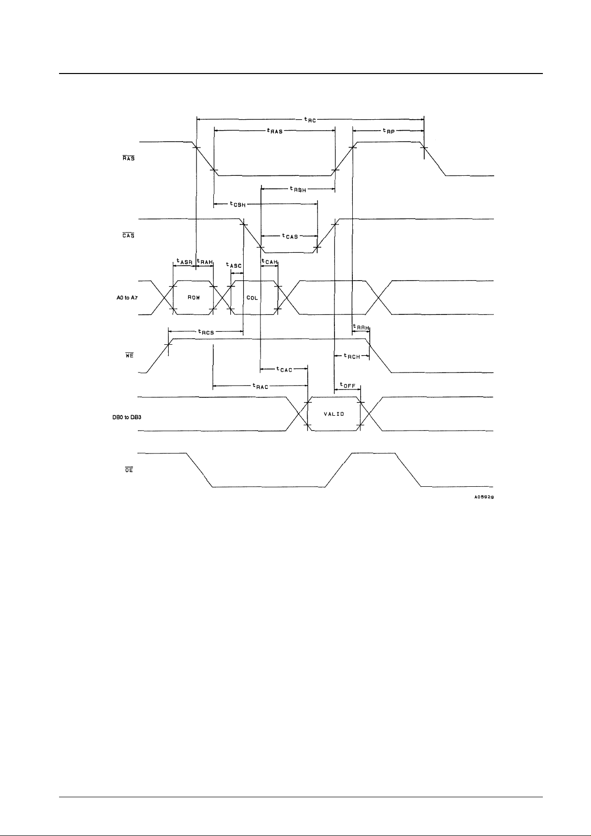
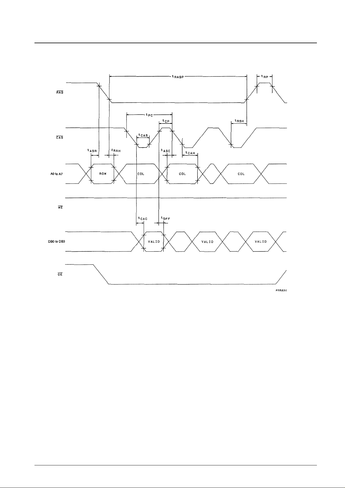
1. DRAM read cycle
No. 5476-7/43
LC78711E
No. 5476-8/43
LC78711E
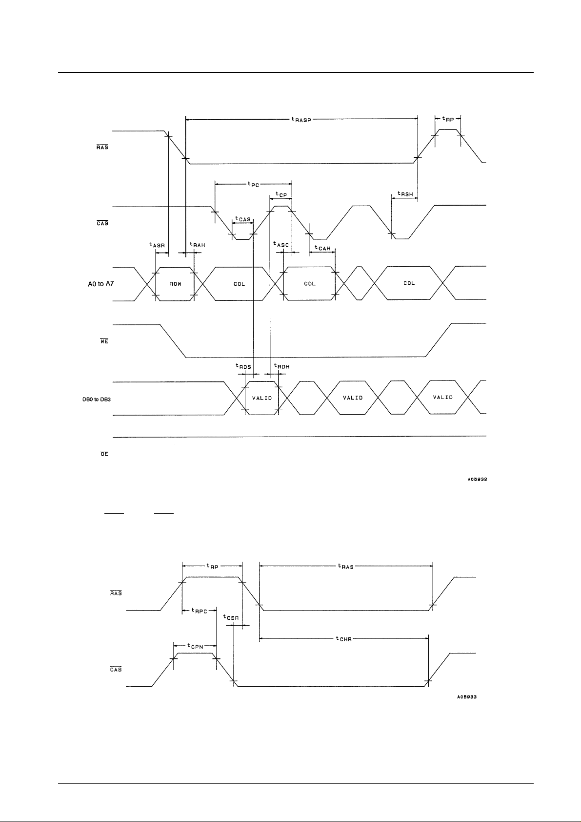
2. DRAM Early write cycle
No. 5476-9/43
LC78711E
3. DRAM page mode read cycle
No. 5476-10/43
LC78711E
4. DRAM page mode write cycle
5. DRAM CAS before RAS refresh cycle
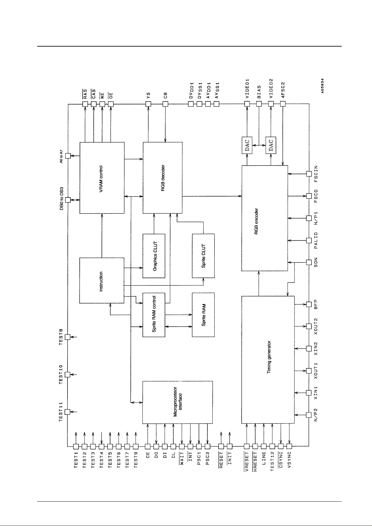
Block Diagram
No. 5476-11/43
LC78711E
Function Overview
1. Crystal clock oscillator; XIN1, XOUT1, XIN2, XOUT2, N/P1, N/P2, FSCO
The XIN1 and XOUT1 pins are connections for an NTSC 14.31818-MHz crystal element, and the XIN2 and XOUT2
pins are connections for a PAL 17.734476-MHz crystal element. The N/P1 pin switches the LC78711E RGB encoder
block between NTSC and PAL modes, and the N/P2 pin switches the decoder block between NTSC and PAL modes.
The FSCO pin outputs a clock signal that is the crystal oscillator frequency divided by 4. The table below enumerates
the pin states vs. the LC78711E operating modes.
2. Display format; N/P1, N/P2, LINE, CSYNC, SON, 4FSC2, FSCIN, VRESET, HRESET, YS, PALID
• The LC78711E supports both NTSC and PAL modes, with the N/P1 and N/P2 pins being used to set the mode. See
item (1) above for the pin states in the NTSC and PAL modes. The LINE pin switches the number of scan lines in a
1-V period.
• The SON, 4FSC2, FSCIN, VRESET, HRESET, YS, and PALID pins are used with the superimpose function. The
4FSC2 pin inputs a 4 × fsc frequency, and the FSCIN pin inputs the fsc frequency. The VRESET and HRESET
pins input the external video signal VSYNC and HSYNC. The internal V and H counters are reset on the falling
edges of these signals, respectively. The image may be disrupted if the 4FSC2 signal is not locked with the
VRESET and HRESET signals. The YS pin is used to switch the video signal. The PALID pin is used for burst
waveform phase matching in PAL mode.
3. DRAM interface
Interface pins: A0 to A7, DB0 to DB3, RAS, CAS, WE, OE
An external 64k × 4-bit DRAM must be used.
4. Video outputs: VIDEO1, VIDEO2
The luminance signal can be acquired from the VIDEO1 pin.
The chrominance signal can be acquired from the VIDEO2 pin.
No. 5476-12/43
LC78711E
XIN1, XOUT1 XIN2, XOUT2 N/P1 N/P2 TV format FSCO
14.31818 MHz * H H NTSC/M 3.579545 MHz
* 17.734476 MHz L L PAL/GBIDH 4.433619 MHz
14.30244 MHz * L H PAL/M 3.575611 MHz
5. Color bar output; CB
If the CB input pin is set high, a color bar signal will be output from the VIDEO1 and VIDEO2 pins. The table below
lists the content of the color bar signal.
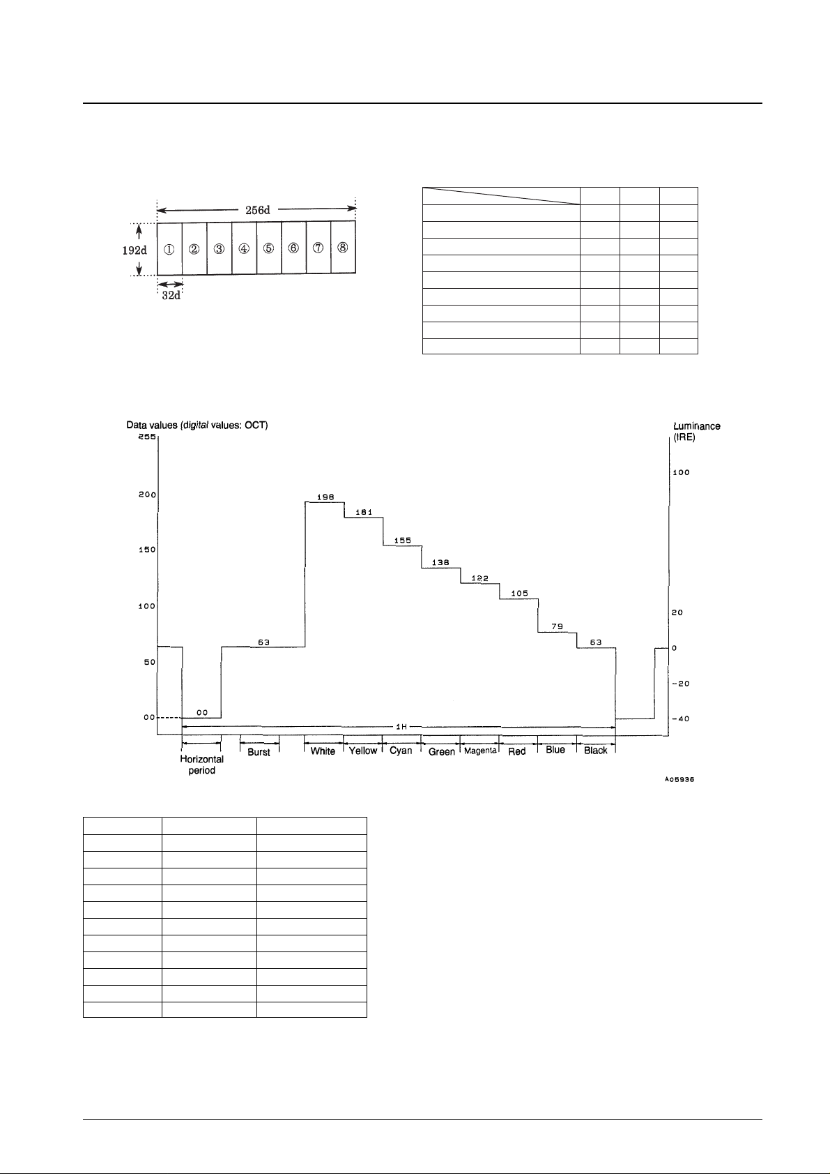
6. Color bar signal output level
• Luminance signal output level (Y signal: VIDEO1, pin 38)
No. 5476-13/43
LC78711E
R G B
➀ White F F F
➁ Gray B B B
➂ Yellow F F O
➃ Cyan O F F
➄ Green O F O
➅ Magenta F O F
➆ Red F O O
➇ Blue O O F
Border (black) O O O
Data value Output voltage (V) Luminance level (IRE)
255 4.990 121.9
220 4.648 100
198 4.434 85.7
181 4.268 74.9
155 4.014 58.4
138 3.848 47.6
122 3.691 37.5
105 3.525 26.7
79 3.271 10.2
63 3.125 0
0 2.500 –40
Note: AVDD1 = 5.00 V
 Loading...