

Page 1
Ordering number : EN4882
N1594TH (OT) B8-1395 No. 4882-1/24
Overview
The LC7868KE is a CMOS LSI that implements the
signal processing and servo control required by compact
disk players, laser disks, CD-V, CD-I and related
products. The LC7868KE provides several types of signal
processing to reduce the cost of CD player units, including
demodulation of the optical pickup EFM signal, deinterleaving and error detection and correction. It also
processes a rich set of servo system commands sent from
the control microprocessor. It can directly interface to the
dedicated serial inputs provided by the Sanyo LC78815
and LC78816 D/A converters.
Functions
• Input signal processing: The LC7868KE takes an HF
signal as input, digitizes (slices) that signal at a precise
level, converts that signal to an EFM signal, and
generates a PLL clock with an average frequency of
4.3218 MHz by comparing the phases of that signal and
a VCO output.
• Precise reference clock and necessary internal timing
generation using an external 16.9344 MHz crystal
oscillator
• Disk motor speed control using a frame phase difference
signal generated from the playback clock and the
reference clock
• Frame synchronization signal detection, protection and
interpolation to assure stable data readout
• EFM signal demodulation and conversion to 8-bit
symbol data
• Subcode data separation from the EFM demodulated
signal and output of that data to an external
microprocessor
• Subcode Q signal output to a microprocessor over the
serial interface after performing a CRC error check (An
LSB first output format can be selected.)
• Demodulated EFM signal buffering in internal RAM to
handle up to ±4 frames of disk rotational jitter
• Demodulated EFM signal reordering in the prescribed
order for data unscrambling and de-interleaving
• Error detection, correction, and flag processing (error
correction scheme: dual C1 plus dual C2 correction)
• The LC7868KE sets the C2 flags based on the C1 flags
and a C2 check, and then performs signal interpolation
or previous value hold depending on the C2 flags. The
interpolation circuit uses a quadruple interpolation
scheme. The output value is locked at zero when four or
more consecutive C2 flags occur.
• Support for command input from a control
microprocessor: commands include track jump, focus
start, disk motor start/stop, muting on/off and track
count (8-bit serial input)
• Built-in digital output circuits.
• Arbitrary track counting to support high-speed data
access
• Zero cross muting
• D/A converter input signal outputs with output data
continuity improved by 4× oversampling and digital
filtering
• Supports most D/A converters
• Built-in digital de-emphasis
• Built-in digital level and peak meter functions
• Support for bilingual applications
Features
• 64-pin QIP (miniature, reduced space package)
• Silicon gate CMOS process (low power)
• Single 5 V power supply (for application in portable end
products)
• Provision of a DEMO pin eases the manufacturing
processes associated with adjustment steps.
LC7868KE
SANYO Electric Co.,Ltd. Semiconductor Bussiness Headquarters
TOKYO OFFICE Tokyo Bldg., 1-10, 1 Chome, Ueno, Taito-ku, TOKYO, 110-8534 JAPAN
Digital Signal Processor for
Compact Disc Players
CMOS LSI
Any and all SANYO products described or contained herein do not have specifications that can handle
applications that require extremely high levels of reliability, such as life-support systems, aircraft’s
control systems, or other applications whose failure can be reasonably expected to result in serious
physical and/or material damage. Consult with your SANYO representative nearest you before using
any SANYO products described or contained herein in such applications.
SANYO assumes no responsibility for equipment failures that result from using products at values that
exceed, even momentarily, rated values (such as maximum ratings, operating condition ranges, or other
parameters) listed in products specifications of any and all SANYO products described or contained
herein.
Page 2
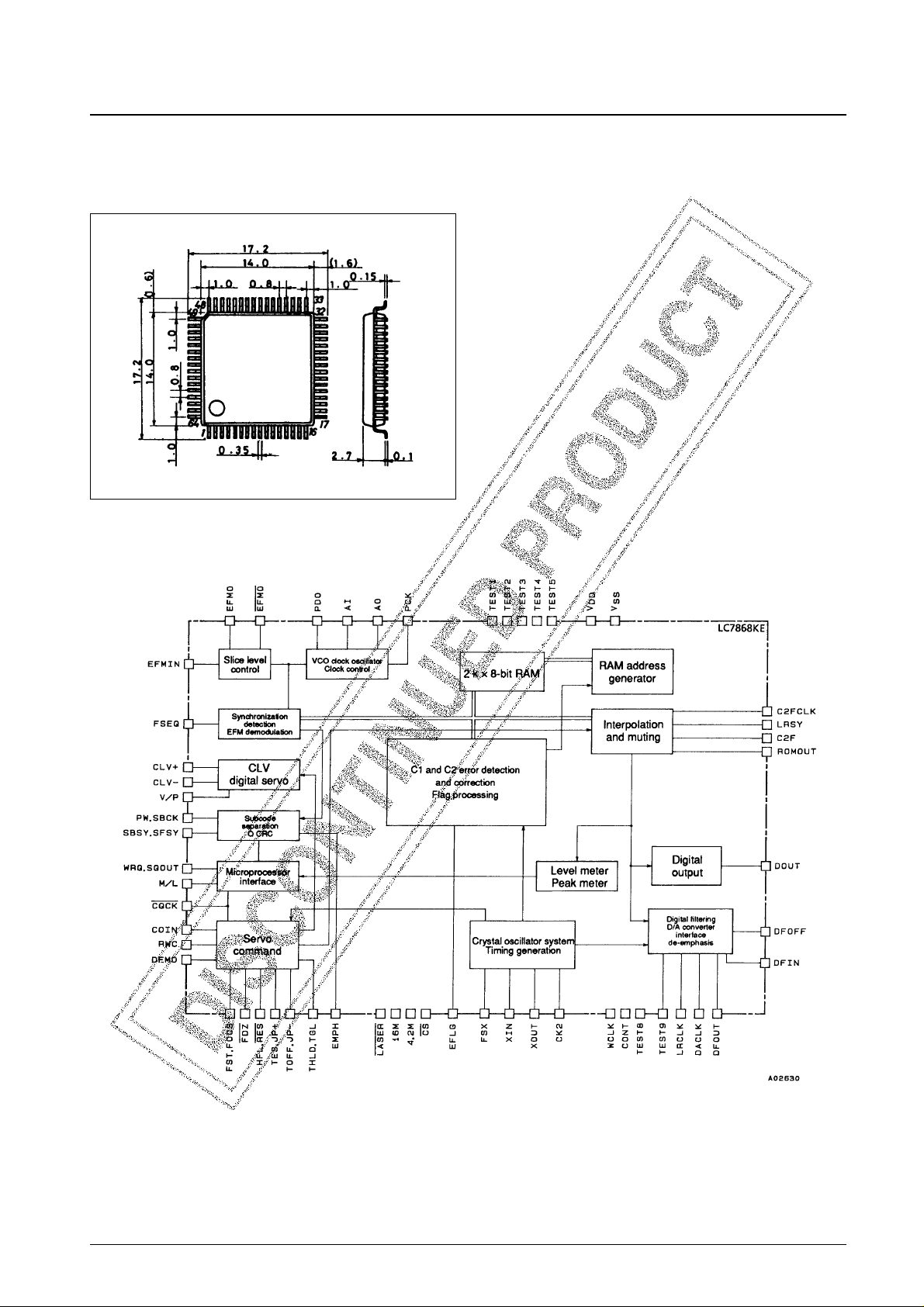
Equivalent Circuit Block Diagram
No. 4882-2/24
LC7868KE
Package Dimensions
unit: mm
3159-QFP64E
SANYO: QFP64E
[LC7868KE]
Page 3
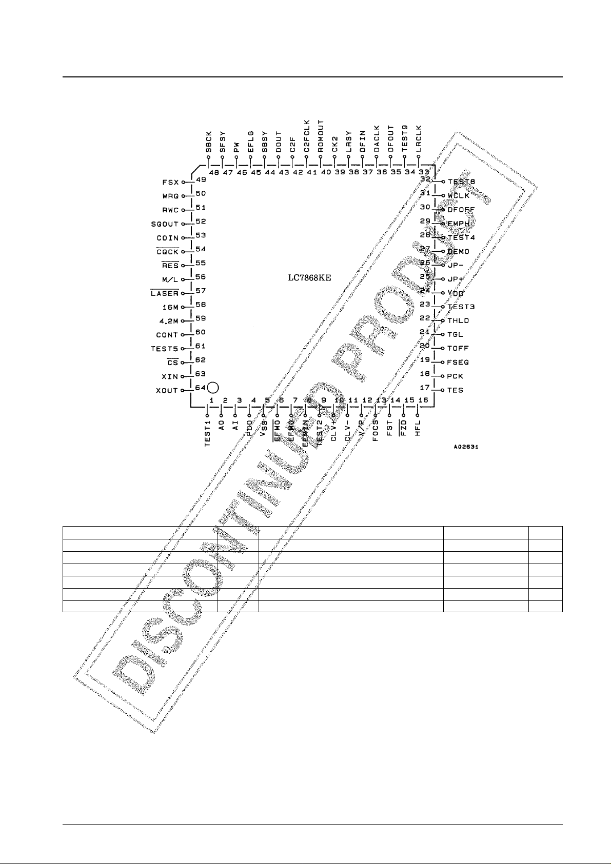
Pin Assignment
Specifications
Absolute Maximum Ratings at Ta = 25°C, VSS= 0 V
No. 4882-3/24
LC7868KE
Parameter Symbol Conditions Ratings Unit
Maximum supply voltage V
DD
max VSS– 0.3 to +7.0 V
Maximum input voltage V
IN
max VSS– 0.3 to VDD+ 0.3 V
Maximum output voltage V
OUT
max VSS– 0.3 to VDD+ 0.3 V
Allowable power dissipation Pd max 300 mW
Operating temperature Topr –30 to +75 °C
Storage temperature Tstg –40 to +125 °C
Top view
Page 4
Allowable Operating Ranges at Ta = 25°C, VSS= 0 V
Electrical Characteristics at Ta = 25°C, V
SS
= 0 V, VDD= 5 V
No. 4882-4/24
LC7868KE
Parameter Symbol Conditions min typ max Unit
Supply voltage V
DD
V
DD
4.5 5.5 V
V
IH
(1) TEST1 to 5, AI, FZD, HFL, DEMO, DFOFF, M/L, RES 0.7 V
DD
V
DD
V
Input high level voltage
V
IH
(2) SBCK, RWC, COIN, CQCK, CS 2.2 V
DD
V
V
IH
(3) EFMIN 0.6 V
DD
V
DD
V
V
IH
(4) TES 0.8 V
DD
V
DD
V
V
IL
(1) TEST1 to 5, AI, FZD, HFL, DEMO, DFOFF, M/L, RES V
SS
0.3 V
DD
V
Input low level voltage
V
IL
(2) SBCK, RWC, COIN, CQCK, CS V
SS
0.8 V
V
IL
(3) EFMIN V
SS
0.4 V
DD
V
V
IL
(4) TES V
SS
0.2 V
DD
V
Data setup time t
setup
COIN, RWC: Figure 1 400 ns
Data hold time t
hold
RWC: Figure 1 400 ns
High level clock pulse width t
WøH
SBCK, CQCK: Figures 1, 2 and 3 400 ns
Low level clock pulse width t
WøL
SBCK, CQCK: Figures 1, 2 and 3 400 ns
Data read access time t
RAC
Figures 2 and 3 0 400 ns
Command transfer time t
RWC
RWC: Figure 1 1000 ns
Subcode Q read enable time t
SQE
Figure 2, with no RWC signal 11.2 ms
Subcode read cycle t sc Figure 3 136 µs
Subcode read enable time t se Figure 3 400 ns
Crystal oscillator frequency fX’tal XIN, XOUT 16.9344 MHz
Operating frequency range
fop (1) AI 2.0 20 MHz
fop (2) EFMIN: V
IN
≥ 1 Vp-p 10 MHz
Parameter Symbol Conditions min typ max Unit
Supply current I
DD
17 30 mA
I
IH
(1)
AI, EFMIN, FZD, TES, SBCK, COIN, CQCK, RES,
5µA
Input high level current
HFL, RWC, M/L: V
IN
= V
DD
IIH(2) TEST1 to 5, DEMO, CS: VIN= VDD= 5.5 V 25 75 µA
Input low level current I
IL
(1)
AI, EFMIN, FZD, TES, SBCK, COIN, CQCK, RES,
–5µA
HFL, RWC, M/L: V
IN
= V
SS
AO, PDO,EFMO, EFMO, CLV+, CLV–, FOCS, FSEQ,
V
OH
(1) PCK, TOFF, TGL, THLD, JP+, JP–, EMPH, EFLG, VDD– 1V
FSX, V/P: I
OH
= –1 mA
Output high level voltage
V
OH
(2) DOUT: IOH= –12 mA VDD– 0.5 V
LASER, SQOUT, 16M, 4.2M, CONT, LRCLK, WRQ,
V
OH
(3)
C2F, DACLK, SFSY, LRSY, SBSY, CK2, PW, ROMOUT,
VDD– 1V
C2FCLK, DFOUT, TEST9, TEST8, WCLK, DFIN:
I
OH
= –0.5 mA
AO, PDO, EFMO, EFMO, CLV
+
, CLV–, FOCS, FSEQ,
V
OL
(1) PCK, TOFF, TGL, THLD, JP+, JP–, EMPH, EFLG, 1 V
FSX, V/P: I
OL
= 1 mA
V
OL
(2) DOUT: IOL= 12 mA 0.5 V
Output low level voltage LASER, SQOUT, 16M, 4.2M, CONT, LRCLK, WRQ,
V
OL
(3)
C2F, DACLK, SFSY, LRSY, SBSY, CK2, PW, ROMOUT,
0.4 V
C2FCLK, DFOUT, TEST9, TEST8, WCLK, DFIN:
I
OL
= 2 mA
V
OL
(4) FST: IOL= 5 mA 0.75 V
Output off leakage current
I
OFF
(1) PDO, FST: VOH= V
DD
5µA
I
OFF
(2) PDO, FST: VOL= V
SS
–5µA
Page 5
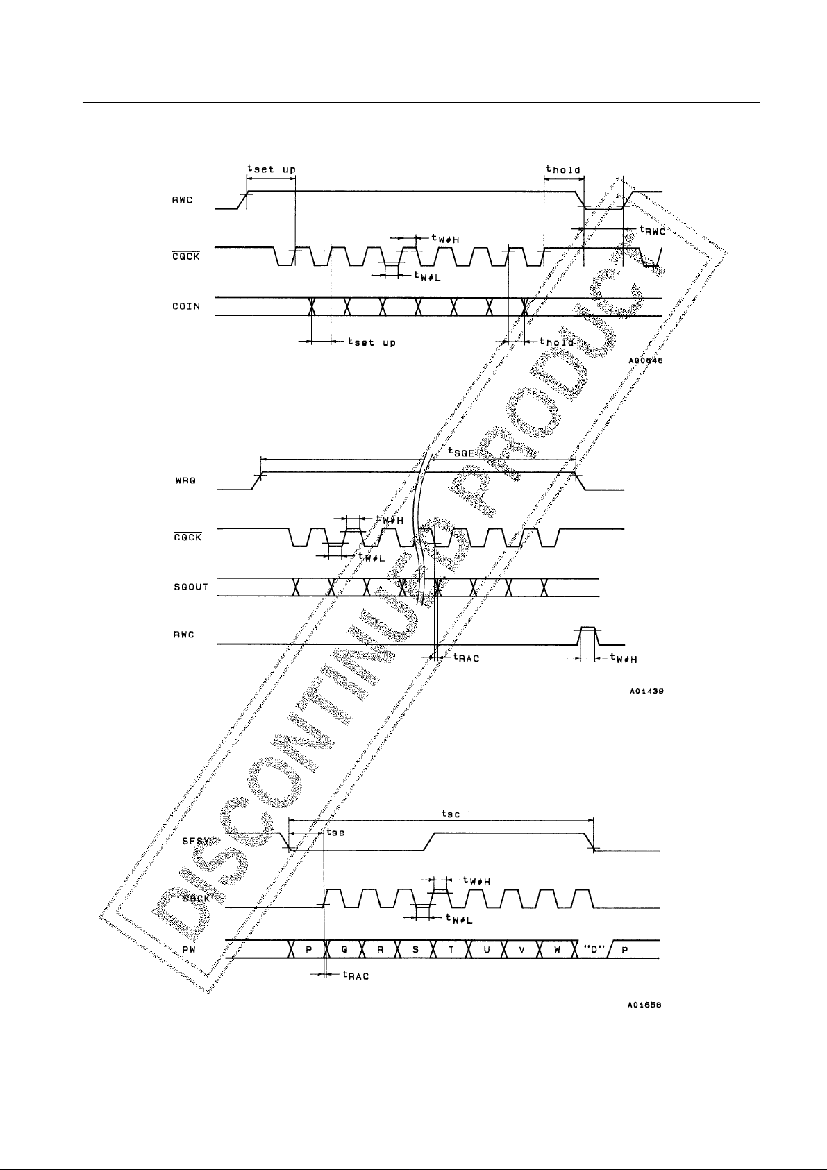
Wave Form
Figure 1 Command Input
Figure 2 Subcode Q Output
Figure 3 Subcode Output
No. 4882-5/24
LC7868KE
Page 6
Pin Functions
No. 4882-6/24
LC7868KE
No. Name I/O Description
1 TEST1 I LSI test pin. Normally left open.
2AO O
3AI I
4 PDO O
5V
SS
— GND
6 EFMO O
7 EFMO O
8 EFMIN I
9 TEST2 I LSI test pin. Normally left open.
10 CLV
+
O
Disk motor control output.
11 CLV
–
O
Three-state output is also possible when specified by microprocessor command.
12 V/P O Outputs a high level during CLV rough servo and a low level during phase control.
13 FOCS O
14 FST O
15 FZD I
16 HFL I
17 TES I
18 PCK O PCK is the 4.3218 MHz monitor pin.
19 FSEQ O
FSEQ outputs a high level when the synchronization (positive FS) detected from the EFM signal matches the counter
synchronization (interpolation FS). (The output is latched for a single frame.)
20 TOFF O
21 TGL O
22 THLD O
23 TEST3 I LSI test pin. Normally left open.
24 V
DD
— +5 V
25 JP
+
O
26 JP
–
O
27 DEMO I Sound output function for end product adjustment manufacturing steps.
28 TEST4 I LSI test pin. Normally left open.
29 EMPH O De-emphasis is required when high.
30 DFOFF I Digital filter on/off switch. Filtering is turned off on a high level input.
31 WCLK O
32 TEST8 O
33 LRCLK O
34 TEST9 O
35 DFOUT O
36 DACLK O
37 DFIN O LSI test pin. Normally left open.
38 LRSY O
39 CK2 O
40 ROMOUT O CD-ROM application output signals
41 C2FCLK O
42 C2F O
43 DOUT O Digital output
44 SBSY O Subcode block synchronization signal
45 EFLG O C1, C2, single and double error correction monitor pin
46 PW O
47 SFSY O
48 SBCK I
49 FSX O 7.35 kHz synchronization signal output
Inputs for the LA9210 internal VCO output. (8.6436 MHz)
Set up PDO so that the frequency increases when the EFM signal and the phase output are positive.
Supply an HF signal with a 1 to 2 Vp-p level to EFMIN. EFMO and EFMO output EFM signals with opposite phases
that passed through an amplitude limiter circuit. These are used for slice level control.
FOCS outputs a high level when the focus servo is off. The lens is lowered by FST, and when FOCS is high the lens is
raised gradually. FOCS is reset when an FZD input occurs. These are used for focus pull-in.
The LC7868KE outputs a kick pulse from JP
+
and JP–in response to a track jump command. A track jump of the
specified number of tracks (1, 2, 4, 16, 32, 64, and 128) is performed.
The LC7868KE outputs a kick pulse from JP
+
and JP–in response to a track jump command. A track jump of the
specified number of tracks (1, 2, 4, 16, 32, 64, and 128) is performed.
The LC7868KE outputs a kick pulse from JP
+
and JP–in response to a track jump command. A track jump of the
specified number of tracks (1, 2, 4, 16, 32, 64, and 128) is performed.
Three-state output is also possible when specified by microprocessor command.
Outputs for an external D/A converter. These include a latch signal, an L/R switching signal, and a sample and hold
signal.
SFSY is the subcode frame synchronization signal. The P, Q, R, S, T, U, V and W subcodes can be read out by
applying 8 clock cycles to SBCK.
Continued on next page.
Page 7
Continued from preceding page.
Pin Applications
1. HF signal input circuit; Pin 8: EFMIN, pin 7: EFMO, pin 6: EFMO
An EFM signal (NRZ) with an optimal slice level can be acquired by inputting the HF signal to EFMIN.
2. PLL clock generation circuit; Pin 4: PDO, Pin 3: AI, Pin 2: AO
A VCO can be constructed by combining the LC7868KE with the Sanyo LA9210. The PDO pin swings in the
positive direction when the VCO phase lags.
No. 4882-7/24
LC7868KE
No. Name I/O Description
50 WRQ O
51 RWC I
52 SQOUT O
53 COIN I
54 CQCK I
55 RES I This pin must be set low briefly after power is first applied.
56 M/L I Similar to pins number 50, 51, 52, 53 and 54 described above.
57 LASER O Output pin controllable by serial data sent from the microprocessor.
58 16M O 16.9344 MHz output pin
59 4.2M O 4.2336 MHz output pin
60 CONT O Output pin controllable by serial data sent from the microprocessor.
61 TEST5 I LSI test pin. Normally left open.
62 CS I Chip select pin. The LC7868KE becomes active when this pin is low. (A pull-down resistor is built-in.)
63 X
IN
I
Connections for a 16.9344 MHz crystal oscillator
64 X
OUT
O
WRQ goes high when the subcode Q data passes the CRC check. An external controller can read out data from
SQOUT by monitoring this pin and applying a CQCK signal. Set M/L to low when data is required LSB first.
The control microprocessor can send commands to the LC7868KE by setting RWC high and then sending command
data synchronized with CQCK.
Page 8
3. 1/2 VCO; Pin 18: PCK
PCK is a monitor pin that outputs an average frequency of 4.3218 MHz, which is the VCO frequency divided by two.
4. Synchronization detection monitor; Pin 19: FSEQ
Pin 19 goes high when the frame synchronization (a positive polarity synchronization signal) from the EFM signal
read in by PCK and the timing generated by the counter (the interpolation synchronization signal) agree. This pin is a
synchronization detection monitor. (It is held high for a single frame.)
5. Servo command function; Pin 51: RWC, pin 53: COIN, pin 54: CQCK, pin 62: CS
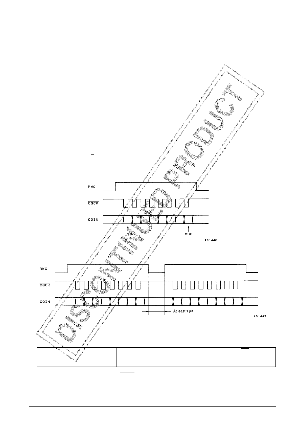
Commands are input to the LC7868KE by setting RWC high and sending commands to the COIN pin in
synchronization with the CQCK clock.
Focus start
Track jump
Mute control 1-byte commands
Disc motor control
Other control commands
Track count 2-byte command
• One-byte commands
• Two-byte commands
Command execution starts on the falling edge of the RWC signal.
• Command noise exclusion
This command allows the noise on the CQCK clock signal to be excluded.
No. 4882-8/24
LC7868KE
MSB LSB Command RES = low
11101111 COMMAND INPUT NOISE EXCLUSION MODE
11101110 RESET NOISE EXCLUSION MODE
○
Page 9

6. Focus servo circuit; Pin 13: FOCS, pin 14: FST, pin 15: FZD, pin 57: LASER
• Laser control
• Focus start
When a focus start instruction (either FOCUS START #1 or FOCUS START #2) is input as a servo command,
first the charge on capacitor C1 is discharged by FST and the objective lens is lowered. Next, the capacitor is
charged by FOCS, and the lens is slowly raised. FZD falls when the lens reaches the focus point. When this signal
is received, FOCS is reset and the focus servo turns on. After sending the command, the microprocessor should
check the in-focus detection signal (the LA9210 DRF signal) to confirm focus before proceeding to the next part of
the program. If focus is not achieved by the time C1 is fully charged, the microprocessor should issue another
focus command and iterate the focus servo operation.
Note: 1. Values in parentheses are for the LASER START #2 command. The only difference is in the FST low period.
2. VAn FZD falling edge will not be accepted during the period that FST is low.
3. After issuing a focus start command, initialization will be performed if RWC is set high. Therefore, do not issue the next command during
focus start until the focus coil drive S curve has completed.
4. When focus cannot be achieved (i.e., when FZD does not go low) the FOCS signal will remain in the high state, so the microprocessor
should initialize the system by issuing a NOTHING command.
5. When the RESET pin is set low, the LASER pin is set high directly.
6. Focus start using the DEMO coil executes a mode #1 focus start.
No. 4882-9/24
LC7868KE
MSB LSB Command RES = low
00001000 FOCUS START #1
10100010 FOCUS START #2
00001010 LASER ON
10001010 LASER OFF ○
00000000 NOTHING
Page 10

7. CLV servo circuit; Pin 10: CLV+, pin 11: CLV–, pin 12: V/P
The CLV
+
pin provides the signal that accelerates the disk in the forward direction and the CLV–pin provides the
signal that decelerates the disk. Commands from the control microprocessor select one of four modes; accelerate,
decelerate, CLV and stop. The table below lists the CLV+and CLV–outputs in each of these modes.
Note: CLV servo control commands can set the TOFF pin low only in CLV mode. That pin will be at the high level
at all other times.
• CLV mode
In CLV mode the LC7868KE detects the disk speed from the HF signal and provides proper linear speed using
several different control schemes by switching the DSP internal modes. The PWM period is 7.35 kHz, the 1/64
duty period is 1.114s, and V/P outputs a high level during rough servo and a low level during phase control.
No. 4882-10/24
LC7868KE
MSB LSB Command RES = low
00000100 DISC MOTOR START (accelerate)
00000101 DISC MOTOR CLV (CLV)
00000110 DISC MOTOR BRAKE (decelerate)
00000111 DISC MOTOR STOP (stop)
○
Mode CLV
+
CLV
–
Accelerate High Low
Decelerate Low High
CLV **
Stop Low Low
Internal mode CLV
+
CLV
–
V/P
Rough servo (velocity too low) High Low High
Rough servo (velocity too high) Low High High
Phase control (PCK locked) PWM PWM Low
Page 11

• Rough servo gain switching
For 8 cm disks, the rough servo mode CLV control gain can be set about 8.5 dB lower than the gain used for 12 cm
disks.
• Phase control gain switching
The phase control gain can be changed by changing the divisor used by the dividers in the stage immediately
preceding the phase comparator.
• CLV three state output
The CLV three state output command allows the CLV to be controlled by a single pin.
No. 4882-11/24
LC7868KE
MSB LSB Command RES = low
10110001 CLV PHASE COMPARATOR DIVISOR: 1/2
10110010 CLV PHASE COMPARATOR DIVISOR: 1/4
10110011 CLV PHASE COMPARATOR DIVISOR: 1/8
1011000 NO CLV PHASE COMPARATOR DIVISOR USED
○
MSB LSB Command RES = low
10110100 CLV THREE STATE OUTPUT
10110101
CLV TWO STATE OUTPUT
○
(the scheme used by previous products)
MSB LSB Command RES = low
10101000 DISC 8 SET
10101001 DISC 12 SET
○
Page 12

• Internal brake modes
— Issuing the internal brake on (C5H) command sets the LC7868KE to internal brake mode. In this mode, the
disk deceleration state can be monitored from the WRQ pin when a brake command (06H) is executed.
— In this mode the disk deceleration state is determined by counting the EFM signal in a single frame to
determine the density, and when the EFM signal count falls under four, the CLV
–
pin is dropped to low. At the
same time the WRQ signal, which functions as a brake completion monitor, goes high. In internal brake
continuous mode, the CLV–pin high level output braking operation continues even after the WRQ brake
completion monitor goes high.
Note that if errors occur in deceleration state determination due to noise in the EFM signal, the problem can be
rectified by changing the EFM signal count from four to eight with the internal brake control command (A3H).
— In TOFF output disabled mode the TOFF pin is held low during internal brake operations.
Note: 1. If focus is lost during the execution of an internal brake command, the pickup must be re-focussed
and then the internal brake command can be reissued.
2. Since incorrect deceleration state determination is possible depending on the EFM signal playback
state (e.g., disk defects, access in progress), we recommend using these functions in combination
with a microprocessor.
8. Track jump circuit; Pin 16: HFL, pin 17: TES, pin 20: TOFF, pin 21: TGL, pin 22: THLD, pin 25: JP
+
, pin 26: JP
–
• The LC7868KE supports the two track jump commands listed below.
The earlier track count function uses the TES signal directly as the internal track counter clock.
To reduce counting errors resulting from noise on the rising and falling edges of the TES signal, the new track
count function prevents noise induced errors by using the combination of the TES and HFL signals, and
implements a more reliable track count function. However, dirt and scratches on the disk can result in HFL signal
dropouts that may result in missing track count pulses. Thus care is required when using this function.
No. 4882-12/24
LC7868KE
MSB LSB Command RES = low
11000101 INTERNAL BRAKE ON
11000100 INTERNAL BRAKE OFF
○
10100011 INTERNAL BRAKE CONT
11001011 INTERNAL BRAKE CONTINUOUS MODE
11001010 RESET CONTINUOUS MODE
○
11001101 TOFF OUTPUT DISABLED MODE
11001100 RESET TOFF OUTPUT DISABLED MODE
○
MSB LSB Command RES = low
00100010 NEW TRACK COUNT (using the TES/HFL combination)
○
00100011 EARLIER TRACK COUNT (directly counts the TES signal)
Page 13

• Track jump commands
When the LC7868KE receives a track jump instruction as a servo command, it first generates accelerating pulses
(period a) and next generates deceleration pulses (period b).
The passage of the braking period (period c) completes the specified jump. During the braking period, the
LC7868KE detects the beam slip direction from the TES and HFL inputs. TOFF is used to cut the components in
the TE signal that aggravate slip. The jump destination track is captured by increasing the servo gain with TGL. In
THLD period TOFF output mode the TOFF signal is held high during the period when THLD is high.
Note: Of the modes related to disk motor control, the TOFF pin only goes low in CLV mode, and will be high
during start, stop, and brake operations. Note that the TOFF pin can be turned on and off independently by
microprocessor issued commands. However, this function is only valid when disk motor control is in CLV
mode. The table lists the relationships between accelerating pulses, deceleration pulses and the braking
period.
No. 4882-13/24
LC7868KE
MSB LSB Command RES = low
10100000 OLD TRACK JUMP
○
10100001 NEW TRACK JUMP
00010001 1 TRACK JUMP IN #1
00010010 1 TRACK JUMP IN #2
00110001 1 TRACK JUMP IN #3
01010010 1 TRACK JUMP IN #4
00010000 2 TRACK JUMP IN
00010011 4TRACK JUMP IN
00010100 16TRACK JUMP IN
00110000 32TRACK JUMP IN
00010101 64TRACK JUMP IN
00010111 128TRACK JUMP IN
00011001 1 TRACK JUMP OUT #1
00011010 1 TRACK JUMP OUT #2
00111001 1 TRACK JUMP OUT #3
01011010 1 TRACK JUMP OUT #4
00011000 2TRACK JUMP OUT
00011011 4TRACK JUMP OUT
00011100 16TRACK JUMP OUT
00111000 32TRACK JUMP OUT
00011101 64TRACK JUMP OUT
00011111 128TRACK JUMP OUT
00010110 256TRACK CHECK
00001111 TOFF
10001111 TON
○
10001100 TRACK JUMP BRAKE
00100001 THLD PERIOD TOFF OUTPUT MODE
00100000 RESET THLD PERIOD TOFF OUTPUT MODE
○
Page 14

• Track jump modes
The table lists the relationships between acceleration pulse output, deceleration pulse output, and the braking
period.
Note: 1. As indicated in the table, actuator signals are not output during the 256 TRACK CHECK function. This is a mode in which the TES signal is
counted in the tracking loop off state. Therefore, feed motor forwarding is required.
2. The servo command register is automatically reset after the track jump sequence (a, b, c) completes.
3. If another track jump command is issued during a track jump operation, the content of that new command will be executed starting immediately.
No. 4882-14/24
LC7868KE
Standard track jump mode New track jump mode
Command
abcabc
1 TRACK JUMP IN (OUT) #1 233 µs 233 µs 60 ms 233 µs 233 µs 60 ms
1 TRACK JUMP IN (OUT) #2 0.5-track jump 233 µs 60 ms 0.5-track jump a period 60 ms
1 TRACK JUMP IN (OUT) #3 0.5-track jump 233 µs Does not occur 0.5-track jump a period Does not occur
1 TRACK JUMP IN (OUT) #4 0.5-track jump 233 µs
60 ms, TOFF = low
0.5-track jump a period
60 ms, TOFF = low
during the c period during the c period
2 TRACK JUMP IN (OUT) None None None 1-track jump a period Does not occur
4 TRACK JUMP IN (OUT) 2-track jump 466 µs 60 ms 2-track jump a period 60 ms
16 TRACK JUMP IN (OUT) 9-track jump 7-track jump 60 ms 9-track jump a period 60 ms
32 TRACK JUMP IN (OUT) 18-track jump 14-track jump 60 ms 18-track jump 14-track jump 60 ms
64 TRACK JUMP IN (OUT) 36-track jump 28-track jump 60 ms 36-track jump 28-track jump 60 ms
128 TRACK JUMP IN (OUT) 72-track jump 56-track jump 60 ms 72-track jump 56-track jump 60 ms
TOFF goes high after 256 tracks are TOFF goes high after 256 tracks are
256 TRACK CHECK jumped. The a and b pulses are not 60 ms jumped. The a and b pulses are not 60 ms
output. output.
TRACK JUMP BRAKE There are no a and b periods. 60ms There are no a and b periods. 60 ms
Page 15

• JP three state output
The JP three state output allows the track jump operation to be controlled from a single pin.
• Track check mode
The LC7868KE will count the specified number of tracks when the microprocessor sends an arbitrary binary value
in the range 16 to 254 after issuing either a track count in or a track count out command.
Note: 1. Once the desired track count has been input in binary, the track count operation is started by the fall of RWC.
2. During a track count operation the TOFF pin goes high and the tracking loop is turned off. Therefore, feed motor forwarding is required.
3. When a track count in/out command is issued the function of the WRQ signal switches from the normal mode subcode Q standby monitor
function to a track count monitor function. This signal goes high when the track count is half completed, and goes low when the count finishes.
The control microprocessor should monitor this signal for a low level to determine when the track count completes.
4. If a two-byte reset command is not issued, the track count operation will be repeated. That is, to skip over 20,000 tracks, issue a track count
200 command once, and then count the WRQ signal 100 times.
5. After performing a track count operation, use the brake command to have the pickup lock onto the track.
No. 4882-15/24
LC7868KE
MSB LSB Command RES = low
10110110 JP THREE STATE OUTPUT
10110111 JP TWO STATE OUTPUT (earlier scheme)
○
MSB LSB Command RES = low
11110000 TRACK COUNT IN
11111000 TRACK COUNT OUT
11111111 TWO BYTE COMMAND RESET
○
Page 16

9. Error flag output; Pin 45: EFLG, pin 49: FSX
The FSX signal is generated by dividing the crystal oscillator clock, and is a 7.35 kHz frame synchronization signal.
The error correction state for each frame is output from EFLG. The playback OK/NG state can be easily determined
from the extent of the high level that appears here.
10. Subcode P, Q, and R to W output circuit; Pin 46: PW, pin 44: SBSY, pin 47: SFSY, pin 48: SBCK
PW is the subcode signal output pin, and all the codes, P, Q, and R to W can be read out by sending eight clocks to
the SBCK pin within 136 µs after the fall of SFSY. The signal that appears on the PW pin changes on the falling
edge of SBCK. If a clock is not applied to SBCK, the P code will be output from PW. SFSY is a signal that is output
for each subcode frame cycle, and the falling edge of this signal indicates standby for the output of the subcode
symbol (P to W). Subcode data P is output on the fall of this signal.
SBSY is a signal output for each subcode block. This signal goes high for the S0 and S1 synchronization signals. The
fall of this signal indicates the end of the subcode synchronization signals and the start of the data in the subcode
block. (EIAJ format)
11. Subcode Q output circuit; Pin 50: WRQ, pin 51: RWC, pin 52: SQOUT, pin 54: CQCK, pin 56: M/L, pin 62: CS
Subcode Q can be read from the SQOUT pin by applying a clock to the CQCK pin.
No. 4882-16/24
LC7868KE
MSB LSB Command RES = low
00001001 ADDRESS FREE
10001001 ADDRESS 1
○
Page 17

Of the eight bits in the subcode, the Q signal is used for song (track) access and display. The WRQ will be high only
if the data passed the CRC error check and the subcode Q format internal address is 1*. The control microprocessor
can read out data from SQOUT in the order shown below by detecting this high level and applying CQCK. When
CQCK is applied the DSP disables register update internally. The microprocessor should give update permission by
setting RWC high briefly after reading has completed. WRQ will fall to low at this time. Since WRQ falls to low
11.2 ms after going high, CQCK must be applied during the high period. Data can be read out in an LSB first format
if the M/L pin is set low, and in an MSB first format if that pin is set low.
Note: * That state will be ignored if an address free command is sent. This is provided to handle CDV applications.
Note: 1. Normally, the WRQ pin indicates the subcode Q standby state. However, it is used for a different monitoring purpose in track count mode.
(See the item on track counting for details.)
2. The LC7868KE becomes active when the CS pin is low, and data is output from the SQOUT pin. When the CS pin is high, the SQOUT pin
goes to the high impedance state.
12. Level meter (LVM) data and peak meter (PKM) data readout
No. 4882-17/24
LC7868KE
MSB LSB Command RES = low
00101011 PKM SET (LVM Reset)
00101100 LVM SET(PKM Reset)
○
00101101 PKM MASK SET
00101110 PKM MASK RESET
○
Page 18

• Level meter (LVM)
— The LVM set (2CH) command sets the LC7868KE to LVM mode.
— LVM data is a 16-bit word in which the MSB indicates the L/R polarity and the low order 15 bits are absolute
value data. A one in the MSB indicates left channel data and a zero indicates right channel data.
— LVM data is appended after the 80 bits of SubQ data, and can be read out by applying 96 clock cycles to the
CQCK pin. Each time LVM data is read out the left/right channel state is inverted. Data is held independently
for both the left and right channels. In particular, the largest value that occurs between readouts for each
channel is held.
• Peak meter (PKM)
— The PKM set (2BH) command sets the LC7868KE to PKM mode.
— PKM data is a 16-bit word in which the MSB is always zero and the low order 15 bits are absolute value data.
This functions detects the maximum value that occurs in the data, whichever channel that value occurs in.
— PKM data is read out in the same manner as LVM data. However, data is not updated as a result of the readout
operation.
— PKM mode SubQ data absolute time is computed by holding the absolute time (ATIME) detected after the
maximum value occurred and sending that value. (Normal operation uses relative time.)
— It is possible to set the LC7868KE to ignore values larger than the already recorded value by issuing the PKM
mask set command, even in PLM mode. This function is cleared by issuing a PLM mask reset command. (This
is used in PK search in a memory track.)
13. Mute control circuit
An attenuation of 12 dB (MUTE –12 dB) or full muting (MUTE ∞ dB) can be applied by issuing the appropriate
command from the table. Since zero cross muting is used, there is no noise associated with this function. Zero cross
is defined for this function as the top seven bits being all ones or all zeros.
14. Bilingual function
• Following a reset or when a stereo (28H) command has been issued, the left and right channel data is output to the
left and right channels respectively.
• When an Lch set (29H) command is issued, the left and right channels both output the left channel data.
• When an Rch set (2AH) command is issued, the left and right channels both output the right channel data.
15. De-emphasis on/off; Pin 29: EMPH
The preemphasis on/off bit in subcode Q control information is output from the EMPH pin. De-emphasis should be
performed when this signal is high.
The LC7868KE includes a digital de-emphasis circuit in its digital filter block. The internal digital de-emphasis
circuit is turned on following a reset. An external de-emphasis circuit can be used by issuing the DEP OFF command
listed in the table.
No. 4882-18/24
LC7868KE
MSB LSB Command RES = low
00000001 MUTE: 0 dB
00000010 MUTE: –12 dB
00000011 MUTE: ∞ dB
○
MSB LSB Command RES = low
00101000 STO CONT
○
00101001 Lch CONT
00101010 Rch CONT
MSB LSB Command RES = low
01101001 DEP OFF
Page 19

16. D/A converter interface; Pin 30: DFOFF, pin 31: WCLK (TEST7) pin 32: TEST (SYSCLK), pin 33: LRRLK, pin
34: DFOUT (DATAR), pin 35: DFOUT (DATAR), pin 36: DACLK
Data for the D/A converter is output MSB first from DFOUT synchronized with the falling edge of DACLK.CONT
and CD-ROM XA reset
When a CD-ROM XA command is issued, data that is neither interpolated nor muted will be output from the
DFOUT and DOUT pins. (This command is used for CD-ROM XA application.) The CD-ROM XA reset command
also functions as a pin 60 CONT reset, so caution is required.
17. CD-ROM outputs; Pin 39: CK2, pin 37: LRSY, pin 40: ROMOUT, pin 42: C2F, pin 41: C2FCLK
Data is output MSB first from the ROMOUT pin in synchronization with the LRSY signal. This data is appropriate
for input to a CD-ROM LSI, since it is not interpolated, previous value held, or processed by the digital filter circuits.
CK2 is a 2.1168 MHz clock, and data is output on the CK2 rising edge. C2F is the flag information for data in 8-bit
units. C2FCLK is the synchronization signal for that flag.
No. 4882-19/24
LC7868KE
MSB LSB Command RES = low
01100010 DF FORM IIS
01100011 DF FORM LC78815
○
01101000 DF FORM B.B
10001000 CD-ROM XA
10001011 CONT AND CD-ROM XA RESET
○
Page 20

LC7868KE - LC89510 interface
18. Digital output circuit; Pin 43: DOUT
This is an output pin for use with a digital audio interface. Data is output in the EIAJ format. This signal has been
processed by the interpolation and muting circuits. This pin has a built-in driver circuit and can directly drive a
transformer.
• The DOUT pin can be locked at the low level by issuing a DOUT OFF command.
• The UBIT information in the DOUT data can be locked at zero by issuing a UBIT OFF command.
19. CONT pin: Pin 60: CONT
The CONT pin goes high when a CONT SET command is issued.
20. Crystal clock oscillator; Pin 63: XIN, pin 64: XOUT
The clock that is used as the time base is generated by connecting a
16.9344 MHz crystal oscillator between these pins. This oscillator
can be turned on and off under command control.
The OSC OFF command turns off both the VCO and crystal
oscillators. The table lists the relationships between the crystal and
VCO oscillators.
No. 4882-20/24
LC7868KE
MSB LSB Command RES = low
01000010 DOUT ON ○
01000011 DOUT OFF
01000000 UBIT ON ○
01000001 UBIT OFF
MSB LSB Command RES = low
10001110 OSC ON ○
10001101 OSC OFF
01100000 VCO 8M ○
01100001 VCO 16M
MSB LSB Command RES = low
00001110 CONT SET Low
10001011 CONT AND CD-ROM XA RESET ○
External
X’tal VCO
16.9344 MHz 8.6436 MHz 17.2872 MHz
Command VCO 8M VCO 8M VCO 16M
Page 21

Recommended crystal clock oscillator component values
21. 4.2M and 16M pins; Pin 59: 4.2M, pin 58: 16M
The 16.9344 MHz external crystal oscillator 16.9344 MHz buffer output signal is output from the 16M pin. That
frequency divided by four (a 4.2336 MHz frequency) is output from the 4.2M pin. When the oscillator is turned off
both these pins will be fixed at either high or low.
22. Reset circuit; Pin 55: RES
When power is first applied, this pin should be briefly set low and then set high. This will set the muting to –∞ dB
and stop the disk motor.
Setting the RES pin low sets the LC7868KE to the settings enclosed in boxes in the table.
23. Adjustment process sound output function; Pin 27: DEMO
No. 4882-21/24
LC7868KE
Manufacturer Oscillator Cin/Cout
CSA-309
5 pF to 10 pF
CITIZEN WATCH CO., LTD. HC-49/U-S
(Cin = Cout)
(16.9344 MHz)
Constant linear velocity servo START BRAKE CLV
Muting control 0 dB –12 dB
Q subcode address conditions Address free
Laser control ON (low) (high)
CONT High
OSC OFF
Track jump mode New
Track count mode Standard
New
Standard
ON
Low
OFF
Address 1
∞
STOP
Page 22

By setting this pin high, muting can be set to 0 dB, the disk motor can be set to CLV, and a focus start operation can
be performed, even without issuing any commands from the control microprocessor. Also, since the LASER pin
becomes active, if the mechanism and servo systems are complete, an EFM signal can be acquired with only this
equipment, and an audio signal can be produced without the presence of a microprocessor.
24. Other pins; Pin 1: TEST1, pin 9: TEST2, pin 23: TEST3, pin 28: TEST4, pin 61: TEST5, pin 37: DFIN
These pins are used for testing the LSI’s internal circuits. Since the pins TEST1 to TEST5 have built-in pull-down
resistors, they can be left open in normal operation.
Circuit Block Operating Descriptions
1. RAM address control
The LC7868KE incorporates an 8-bit × 2 k-word RAM on chip. This RAM is used as a buffer memory, and has an
EFM demodulated data jitter handling capacity of ±4 frames. The LC7868KE continuously checks the remaining
buffer capacity and controls the data write address to fall in the center of the buffer capacity by making fine
adjustments to the PCK side of the CLV servo circuit and the frequency divisor. If the ±4 frame buffer capacity is
exceeded, the LC7868KE forcibly sets the write address to the ±0 position. However, since the errors that occur due
to this operation cannot be handled with error flag processing, the IC applies muting to the output for a 128 frame
period.
2. C1 and C2 error correction
The EFM demodulated data is written to internal RAM to compensate for jitter, and the LC7868KE performs the
following processing with a constant timing based on the crystal oscillator clock. First, the LC7868KE performs C1
error checking and correction in the C1 block, determines the C1 flags, and writes the C1 flag register. Next, the
LC7868KE performs C2 error checking and correction in the C2 block, determines the C2 flags, and writes data to
internal RAM.
Note: 1. If the positions of the errors determined by the C2 check agree with the those specified by the C1 flags, the correction is performed and the
flags are cleared. However, if the number of C1 flags is 7 or higher, C2 correction may fail. In this case correction is not performed and the C1
flags are taken as the C2 flags without change. Error correction is not possible if one error position agrees and the other does not.
Furthermore, if the number of C1 flags is 5 or under, the C1 check result can be seen as unreliable. Accordingly, the flags will be set in this
case. Cases where the number of C1 flags is 6 or more are handled in the same way, and the C1 flags are taken as the C2 flags without
change. When there is not even one agreement between the error positions, error correction is, of course, impossible. Here, if the number of
C1 flags was 2 or under, data that was seen as correct after C1 correction is now seen as incorrect data. The flags are set in this case. The
other C1 flags are taken as the C2 flags without change.
2. When data is determined to have three or more errors and be uncorrectable, correction is, of course, impossible. Here, if the number of C1
flags was 2 or under, data that was seen as correct after C1 correction is now seen as incorrect data. The flags are set in this case. The other
C1 flags are taken as the C2 flags without change.
No. 4882-22/24
LC7868KE
C1 flag Error correction and flag processing
No errors No correction required · Flag reset
1 error Correction · Flag reset
2 errors Correction · Flag set
3 errors or more Correction not possible · Flag set
Position Division ratio or processing
–4 or less Force to ±0
–3 589
–2 589 Increase ratio
–1 589
±0 588 Standard ratio
+1 587
+2 587 Decrease ratio
+3 587
+4 or more Force to ±0
C2 flag Error correction and flag processing
No errors No correction required · Flag reset
1 error Correction · Flag reset
2 errors Depends on C1
*1
3 errors or more Depends on C1
*2
Page 23

Differences between the LC7868E and the LC7868KE
1. New functions
• CLV phase comparator divisor function (divisors of 2, 4, and 8)
• CLV three state output
• JP three state output
2. New commands
• Command input
• CLV servo
• Track jump
• Internal brake mode
3. Changed specification
• The “c” periods (braking periods) during track jump operations have all been changed from 24 ms to 60 ms.
No. 4882-23/24
LC7868KE
MSB LSB Command RES = low Function
11101111 COMMAND INPUT NOISE EXCLUSION MODE Excludes noise from the CQCK signal.
11101110
RESET NOISE EXCLUSION MODE
○
(earlier product scheme)
MSB LSB Command RES = low Function
11001011 INTERNAL BRAKE CONTINUOUS MODE
11001010
RESET CONTINUOUS MODE
○
(earlier product scheme)
11001101 TOFF OUTPUT DISABLED MODE
11001100
RESET TOFF OUTPUT DISABLED MODE
○
(earlier product scheme)
MSB LSB Command RES = low Function
10110001 CLV PHASE COMPARATOR DIVISOR: 1/2
10110010 CLV PHASE COMPARATOR DIVISOR: 1/4
10110011 CLV PHASE COMPARATOR DIVISOR: 1/8
10110000
NO CLV PHASE COMPARATOR DIVISOR USED
○
(earlier product scheme)
10110100 CLV THREE STATE OUTPUT MODE
10110101
RESET THREE STATE OUTPUT MODE
○
(earlier product scheme)
The earlier product compared the phase for
each 7.35 kHz cycle. A new frequency
divisor function has been added.
CLV servo can be controlled from a single
pin since a three state output function has
been added to the CLV
+
pin (and to the
CLV
–
pin as well).
MSB LSB Command RES = low Function
10110110 JP THREE STATE OUTPUT
10110111
RESET THREE STATE OUTPUT MODE
○
(earlier product scheme)
01010010 1 TRACK JUMP IN #4
01011010 1 TRACK JUMP OUT #4
00100001 THLD PERIOD TOFF OUTPUT MODE
00100000 RESET THLD PERIOD TOFF OUTPUT MODE
○
The track jump function can be controlled
from a single pin since a three state output
function has been added to the JP
+
pin (and
to the JP
–
pin as well).
TOFF is set low during the track jump “c”
period.
TOFF is set high during the track jump THLD
period.
TOFF is set high during the track jump THLD
period.The LC7868KE remains in continuous
brake operation mode even after WRQ goes
high.
TOFF goes low during internal brake
operation.
Page 24

No. 4882-24/24
LC7868KE
This catalog provides information as of August, 1998. Specifications and information herein are subject to
change without notice.
Specifications of any and all SANYO products described or contained herein stipulate the performance,
characteristics, and functions of the described products in the independent state, and are not guarantees
of the performance, characteristics, and functions of the described products as mounted in the customer’s
products or equipment. To verify symptoms and states that cannot be evaluated in an independent device,
the customer should always evaluate and test devices mounted in the customer’s products or equipment.
SANYO Electric Co., Ltd. strives to supply high-quality high-reliability products. However, any and all
semiconductor products fail with some probability. It is possible that these probabilistic failures could
give rise to accidents or events that could endanger human lives, that could give rise to smoke or fire,
or that could cause damage to other property. When designing equipment, adopt safety measures so
that these kinds of accidents or events cannot occur. Such measures include but are not limited to protective
circuits and error prevention circuits for safe design, redundant design, and structural design.
In the event that any and all SANYO products described or contained herein fall under strategic
products (including services) controlled under the Foreign Exchange and Foreign Trade Control Law of
Japan, such products must not be exported without obtaining export license from the Ministry of
International Trade and Industry in accordance with the above law.
No part of this publication may be reproduced or transmitted in any form or by any means, electronic or
mechanical, including photocopying and recording, or any information storage or retrieval system,
or otherwise, without the prior written permission of SANYO Electric Co., Ltd.
Any and all information described or contained herein are subject to change without notice due to
product/technology improvement, etc. When designing equipment, refer to the “Delivery Specification”
for the SANYO product that you intend to use.
Information (including circuit diagrams and circuit parameters) herein is for example only; it is not
guaranteed for volume production. SANYO believes information herein is accurate and reliable, but
no guarantees are made or implied regarding its use or any infringements of intellectual property rights
or other rights of third parties.
 Loading...