

SANYO LC78632RE Datasheet
CMOS LSI
Ordering number : EN*5826
D3097HA (OT) No. 5826-1/9
SANYO Electric Co.,Ltd. Semiconductor Bussiness Headquarters
TOKYO OFFICE Tokyo Bldg., 1-10, 1 Chome, Ueno, Taito-ku, TOKYO, 110 JAPAN
Compact Disk Player DSP
LC78632RE
Overview
The LC78632RE is a compact disc D/A signal-processing
LSI for Video-CD players that provides a variable clock
error correction (VCEC) mode. The LC78632RE
demodulates the EFM signal from the optical pickup and
performs de-interleaving, error detection, error correction,
digital filtering, and other processing. The LC78632RE
includes an on-chip 1-bit D/A converter, and executes
commands sent from a control microprocessor.
Features
• VCEC support
• Built-in PLL circuit for EFM detection (supports 4×
playback)
• 18KB RAM on chip
• Error detection and correction (corrects two errors in C1
and four errors in C2)
• Frame jitter margin: ±8 frames
• Frame synchronization signal detection, protection, and
insertion
• Dual interpolation adopted in the interpolation circuit.
• EFM data demodulation
• Subcode demodulation
• Zero-cross muting adopted
• Servo command interface
• 2fs digital filter
• Digital de-emphasis
• Built-in independent left- and right-channel digital
attenuators (239 attenuation steps)
• Supports the bilingual function
• Left/right swap function
• Built-in 1-bit D/A converter (third-order ∆∑ noise
shaper, PWM output)
• Built-in digital output circuit
• CLV servo
• Arbitrary track jumping (of up to 255 tracks)
• Variable sled voltage (four levels)
• Six extended I/O ports and 2 extended output ports
• Built-in oscillator circuit using an external 16.9344 MHz
or 33.8688 MHz (for 4× playback) element
• Supply voltage: 4.5 to 5.5 V
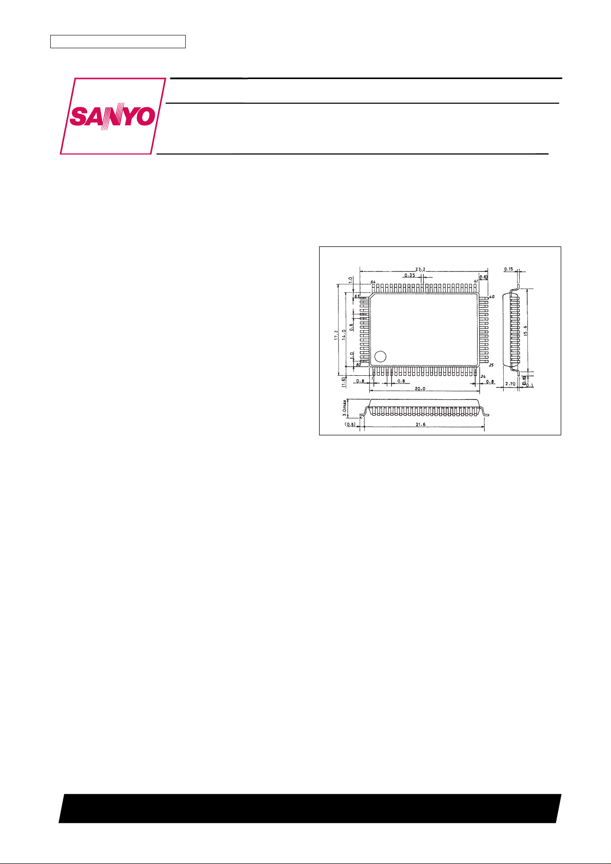
Package Dimensions
unit: mm
3174-QFP80E
Preliminary
SANYO: QFP80E
[LC78632RE]
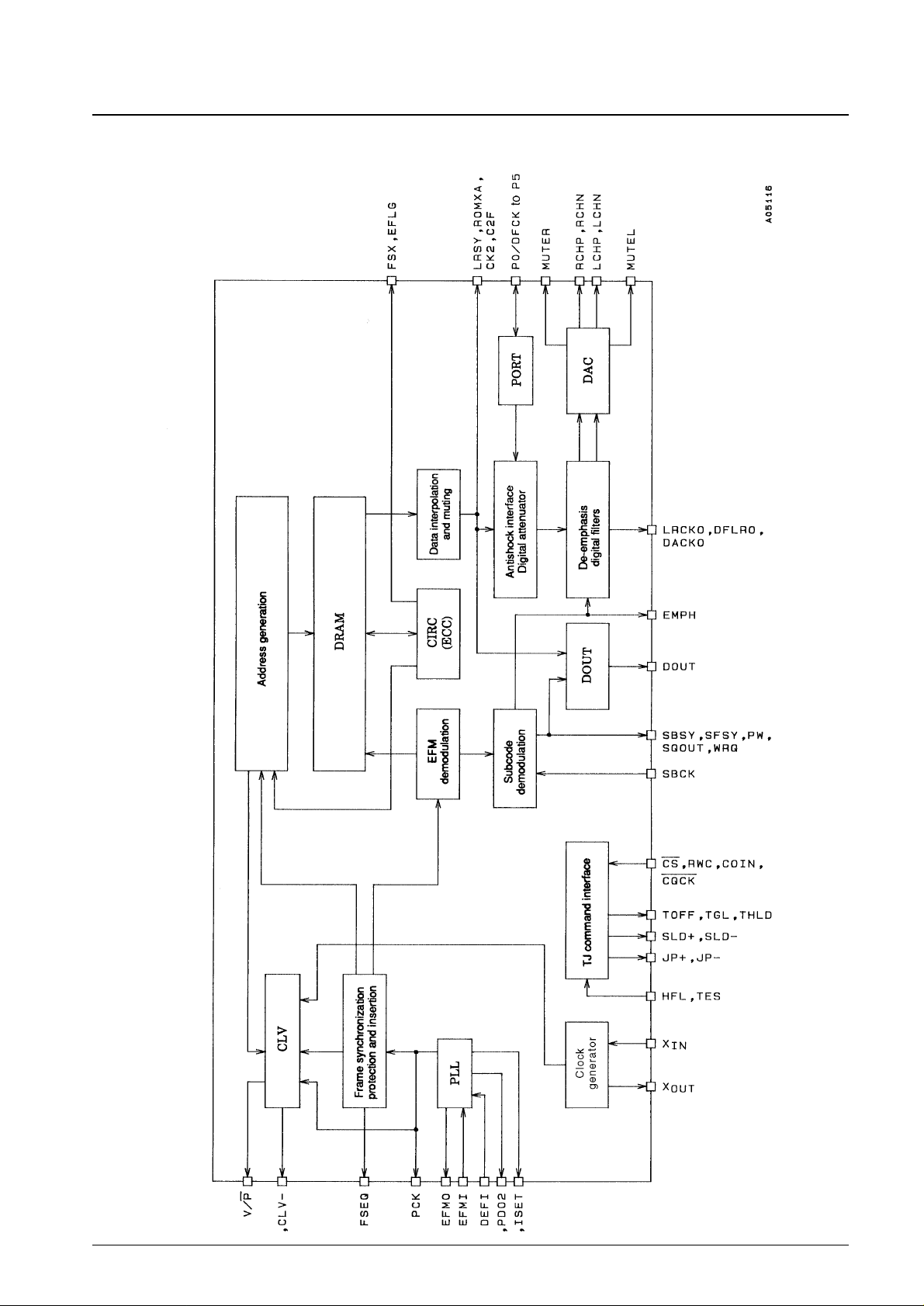
Equivalent Circuit Block Diagram
No. 5826-2/9
LC78632RE
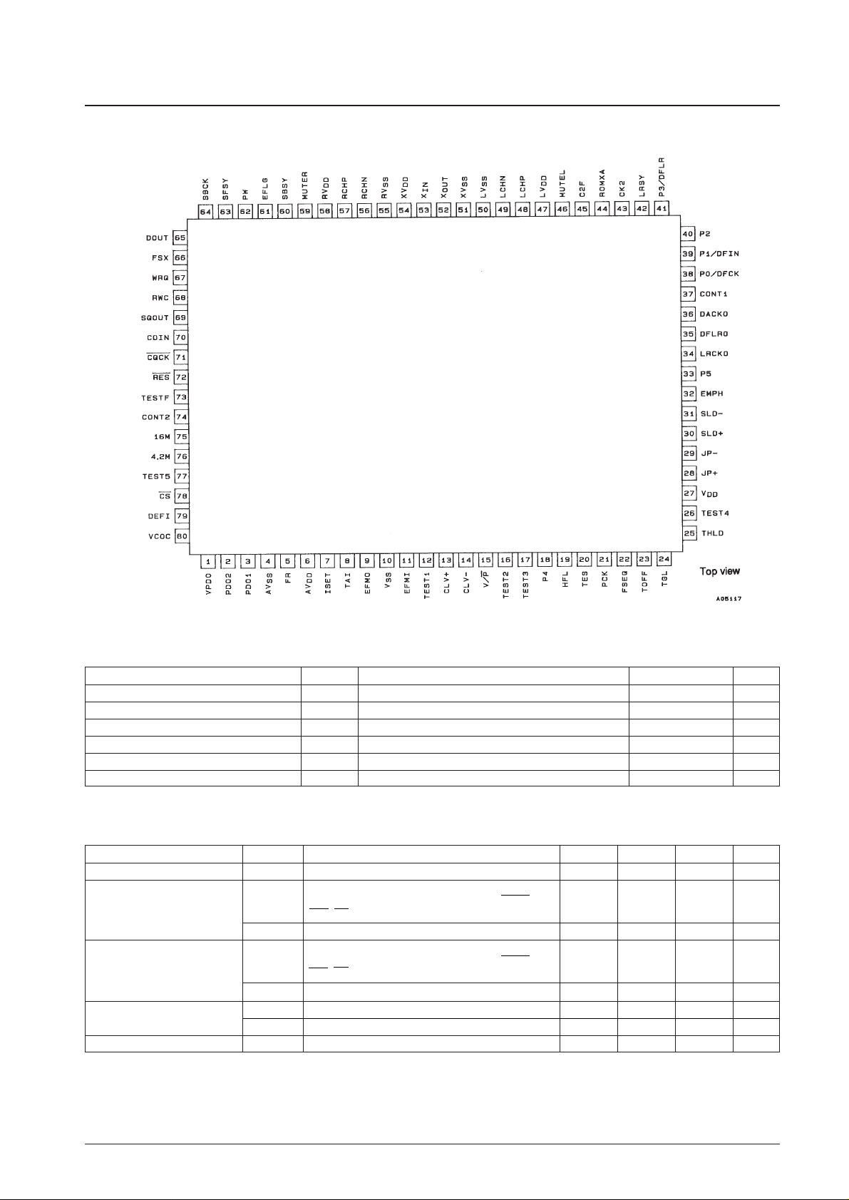
Pin Assignment
Absolute Maximum Ratings at Ta = 25°C, VSS= 0 V
Allowable Operating Ranges at Ta = 25°C, VSS= 0 V
No. 5826-3/9
LC78632RE
Parameter Symbol Conditions Ratings Unit
Maximum supply voltage V
DD
max –0.3 to +7.0 V
Input voltage V
IN
–0.3 to VDD+ 0.3 V
Output voltage V
OUT
–0.3 to VDD+ 0.3 V
Allowable power dissipation Pd max 470 mW
Operating temperature Topr –30 to +75 °C
Storage temperature Tstg –40 to +125 °C
Parameter Symbol Conditions min typ max Unit
Supply voltage V
DD
VDD, AVDD, XVDD, LVDD, RV
DD
4.5 5.0 5.5 V
TEST1 to TEST5, TAI, HFL, TES, P0/DFCK, P1/DFIN,
Input high-level voltage
VIH1 P2, P3/DFLR, P4, P5, SBCK, RWC, COIN, CQCK, 0.7 V
DD
V
DD
V
RES, CS, X
IN
, DEFI
V
IH
2 EFMI 0.6 V
DD
V
DD
V
TEST1 to TEST5, TAI, HFL, TES, P0/DFCK, P1/DFIN,
Input low-level voltage
VIL1 P2, P3/DFLR, P4, P5, SBCK, RWC, COIN, CQCK, 0 0.3 V
DD
V
RES, CS, X
IN
, DEFI
V
IL
2 EFMI 0 0.4 V
DD
V
Data setup time
t
SU
COIN, RWC: Figures 1 and 4 400 ns
t
PRS
RWC: Figure 4 100 ns
Data hold time t
HD
COIN, RWC: Figures 1 and 4 400 ns
Continued on next page.
LC78632RE
 Loading...