

SANYO LC78620E Datasheet

92895HA (OT) No. 5130-1/34
Overview
The LC78620E is a CMOS LSI that implements the signal
processing and servo control required by compact disk
players, laser disks, CD-V, CD-I and related products. The
LC78620E provides several types of signal processing,
including demodulation of the optical pickup EFM signal,
de-interleaving, error detection and correction, and digital
filters that can help reduce the cost of CD player units. It
also processes a rich set of servo system commands sent
from the control microprocessor. It also incorporates an
EFM-PLL circuit and a one-bit D/A converter.
Functions
• Input signal processing: The LC78620E takes an HF
signal as input, digitizes (slices) that signal at a precise
level, converts that signal to an EFM signal, and
generates a PLL clock with an average frequency of
4.3218 MHz by comparing the phases of that signal and
an internal VCO.
• Precise reference clock and necessary internal timing
generation using an external 16.9344 MHz crystal
oscillator
• Disk motor speed control using a frame phase difference
signal generated from the playback clock and the
reference clock
• Frame synchronization signal detection, protection and
interpolation to assure stable data readout
• EFM signal demodulation and conversion to 8-bit
symbol data
• Subcode data separation from the EFM demodulated
signal and output of that data to an external
microprocessor
• Subcode Q signal output to a microprocessor over the
serial I/O interface after performing a CRC error check
• Demodulated EFM signal buffering in internal RAM to
handle up to ±4 frames of disk rotational jitter
• Demodulated EFM signal reordering in the prescribed
order for data unscrambling and de-interleaving
• Error detection, correction, and flag processing (error
correction scheme: dual C1 plus dual C2 correction)
• The LC78620E sets the C2 flags based on the C1 flags
and a C2 check, and then performs signal interpolation
or muting depending on the C2 flags. The interpolation
circuit uses a quadruple interpolation scheme. The
output value converges to the muting level when four or
more consecutive C2 flags occur.
• Support for command input from a control
microprocessor: commands include track jump, focus
start, disk motor start/stop, muting on/off and track
count (8 bit serial input)
• Built-in digital output circuits.
• Arbitrary track counting to support high-speed data
access
• Zero cross muting
• D/A converter outputs with data continuity improved by
8× oversampling digital filters. (These filters function as
4× oversampling filters during double-speed playback.)
• Built-in third-order ∑∆ D/A converters (PWM output)
• Built-in digital attenuator (8 bits – alpha, 239 steps)
• Built-in digital de-emphasis
• Built-in digital level and peak meter functions
• Support for bilingual applications
Features
• 80-pin QIP (miniature, reduced space package)
• Silicon gate CMOS process (for low power)
• 5 V single-voltage power supply (for use in portable
products)
Package Dimensions
unit: mm
3174-QFP80E
Preliminary
SANYO: QIP80E
[LC78620E]
Ordering number : EN*5130
CMOS LSI
LC78620E
Compact Disc Player DSP
SANYO Electric Co.,Ltd. Semiconductor Bussiness Headquarters
TOKYO OFFICE Tokyo Bldg., 1-10, 1 Chome, Ueno, Taito-ku, TOKYO, 110-8534 JAPAN

Equivalent Circuit Block Diagram
Pin Assignment
No. 5130-2/34
LC78620E
Specifications
Absolute Maximum Ratings at Ta = 25°C, VSS= 0 V
Allowable Operating Ranges at Ta = 25°C, VSS= 0 V
Note: Due to the structure of this LSI, an identical voltage must be supplied to all the power supply pins.
Electrical Characteristics at Ta = 25°C, VDD= 5 V, VSS= 0 V
No. 5130-3/34
LC78620E
Parameter Symbol Conditions Ratings Unit
Maximum supply voltage V
DD
max VSS– 0.3 to VSS+ 7.0 V
Maximum input voltage V
IN
max VSS– 0.3 to VDD+ 0.3 V
Maximum output voltage V
OUT
max VSS– 0.3 to VDD+ 0.3 V
Allowable power dissipation Pd max 300 mW
Operating temperature Topr –20 to +75 °C
Storage temperature Tstg –40 to +125 °C
Parameter Symbol Conditions min typ max Unit
Supply voltage V
DD
VDD, XVDD, LVDD, RVDD, VV
DD
4.5 5.5 V
DEFI, FZD, ASDACK, ASDFIN, ASDFIR, ASLRCK,
Input high level voltage
VIH(1) COIN, RES, HFL, TES, SBCK, RWC, CQCK, TAI, 0.7 V
DD
V
DD
V
TEST1 to TEST5, DEMO, CS
VIH(2) EFMIN 0.6 V
DD
V
DD
V
DEFI, FZD, ASDACK, ASDFIN, ASDFIR, ASLRCK,
Input low level voltage
VIL(1) COIN, RES, HFL, TES, SBCK, RWC, CQCK, TAI, 0 0.3 V
DD
V
TEST1 to TEST5, DEMO, CS
VIL(2) EFMIN 0 0.4 V
DD
V
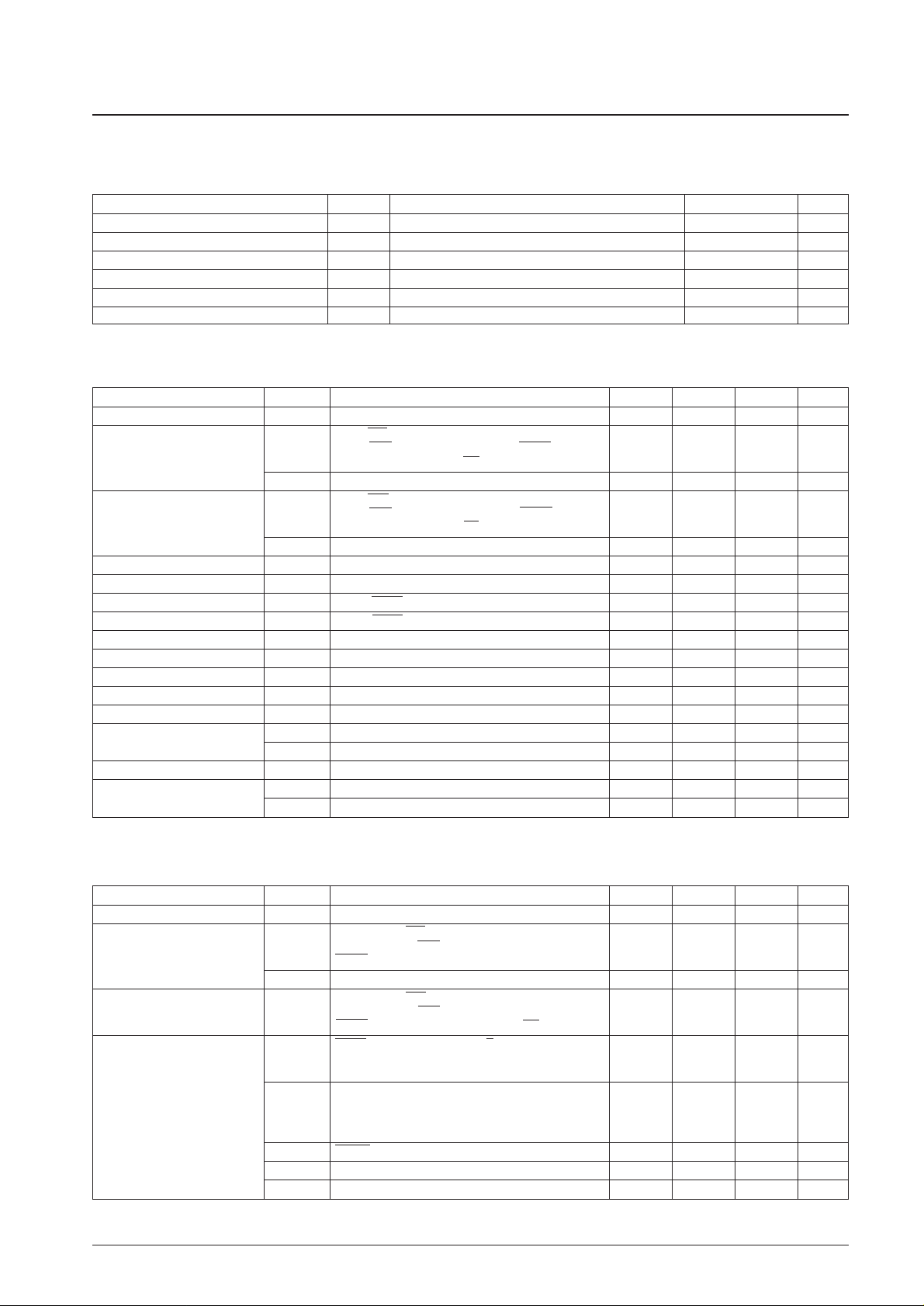
Data setup time t
set up
COIN, RWC: Figure 1 400 ns
Data hold time t
hold
COIN, RWC: Figure 1 400 ns
High level clock pulse width t
WøH
SBCK, CQCK: Figures 1, 2 and 3 400 ns
Low level clock pulse width t
WøL
SBCK, CQCK: Figures 1, 2 and 3 400 ns
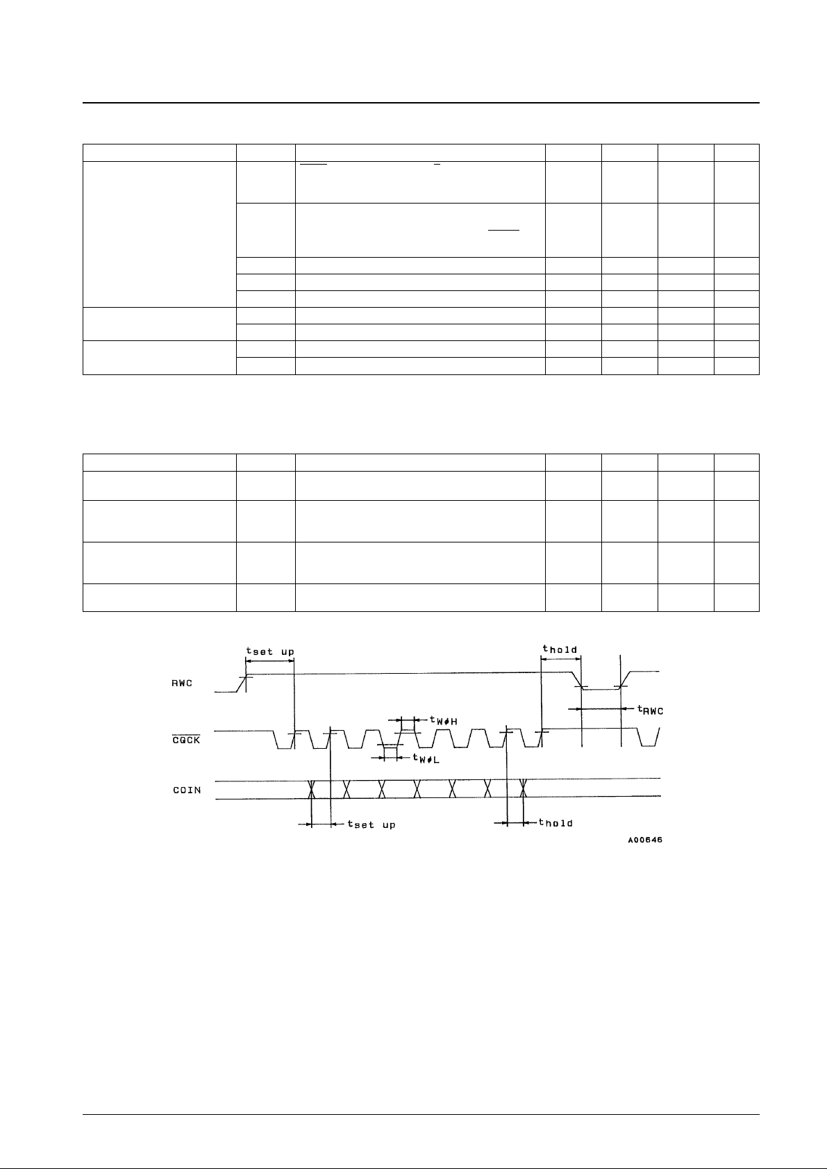
Data read access time t
RAC
SQOUT, PW: Figures 2 and 3 0 400 ns
Command transfer time t
RWC
RWC: Figure 1 1000 ns
Subcode Q read enable time t
SQE
WRQ: Figure 2, with no RWC signal 11.2 ms
Subcode read cycle time t
sc
SFSY: Figure 3 136 µs
Subcode read enable time t
se
SFSY: Figure 3 400 ns
Input level
V
IN
(1) EFMIN 1.0 Vp-p
V
IN
(2) XIN: Input capacitor coupled 1.0 Vp-p
Operating frequency range fop EFMIN 10 MHz
Crystal oscillator frequency
fX (1) X
IN
, X
OUT
: In 16M mode 16.9344 MHz
fX (2) X
IN
, X
OUT
: In 32M mode 33.8688 MHz
Parameter Symbol Conditions min typ max Unit
Current drain I
DD
30 45 mA
DEFI, EFMIN, FZD, ASDACK, ASDFIN, ASDFIR,
Input high level current
IIH(1) ASLRCK, COIN, RES, HFL, TES, SBCK, RWC, 5 µA
CQCK: V
IN
= 5 V
I
IH
(2) TAI, TEST1 to TEST5, DEMO, CS: VIN= VDD= 5.5 V 25 75 µA
DEFI, EFMIN, FZD, ASDACK, ASDFIN, ASDFIR,
Input low level current I
IL
ASLRCK, COIN, RES, HFL, TES, SBCK, RWC, –5 µA
CQCK, TAI, TEST1 to TEST5, DEMO, CS: V
IN
= 0 V
EFMO, EFMO, CLV
+
, CLV–, V/P, FOCS, PCK, FSEQ,
V
OH
(1) TOFF, TGL, THLD, JP+, JP–, EMPH, EFLG, FSX: 4 V
I
OH
= –1 mA
MUTEL, MUTER, LRCKO, DFORO, DFOLO, DACKO,
V
OH
(2)
TST10, LRSY, CK2, ROMXA, C2F, SBSY, PW, SFSY,
4 V
Output high level voltage
WRQ, SQOUT, TST11, 16M, 4.2M, CONT:
I
OH
= –0.5 mA
V
OH
(3) LASER: IOH= –1 mA 4.6 V
V
OH
(4) DOUT: IOH= –12 mA 4.5 V
V
OH
(5) LCHP, RCHP, LCHN, RCHN: IOH= –1mA 3.0 4.5 V
Continued on next page.
Continued from preceding page.
Note: For guaranteed operation, the VCO oscillator frequency range adjustment resistor FR must be a 5.10 kΩ±1.0% tolerance resistor.
One-Bit D/A Converter Analog Characteristics
at Ta = 25°C, VDD= LVDD= RVDD= 5 V, VSS= LVSS= RVSS= 0 V
Note: Measured with the normal-speed playback mode in the Sanyo one-bit D/A converter block reference digital attenuator circuit set to EE (hexadecimal).
Figure 1 Command Input
No. 5130-4/34
LC78620E
Parameter Symbol Conditions min typ max Unit
Total harmonic distortion THD + N
LCHP, RCHP, LCHN, RCHN; 1 kHz: 0 dB data input,
0.008 0.010 %
using the 20 kHz low-pass filter (AD725D built in)
LCHP, RCHP, LCHN, RCHN; 1 kHz: –60 dB data input,
Dynamic range DR using the 20 kHz low-pass filter and the A filter 84 88 dB
(AD725D built in)
LCHP, RCHP, LCHN, RCHN; 1 kHz: 0 dB data input,
Signal-to-noise ratio S/N using the 20 kHz low-pass filter and the A filter 98 100 dB
(AD725D built in)
Crosstalk CT
LCHP, RCHP, LCHN, RCHN; 1 kHz: 0 dB data input,
96 98 dB
using the 20 kHz low-pass filter (AD725D built in)
Parameter Symbol Conditions min typ max Unit
EFMO, EFMO, CLV
+
, CLV–, V/P, FOCS, PCK, FSEQ,
V
OL
(1) TOFF, TGL, THLD, JP+, JP–, EMPH, EFLG, FSX: 1 V
I
OL
= 1 mA
MUTEL, MUTER, LRCKO, DFORO, DFOLO, DACKO,
V
OL
(2)
TST10, LRSY, CK2, ROMXA, C2F, SBSY, PW, SFSY,
0.4 V
Output low level voltage
WRQ, SQOUT, TST11, 16M, 4.2M, CONT, LASER:
I
OL
= 2 mA
V
OL
(3) DOUT: IOL= 12 mA 0.5 V
V
OL
(4) FST: IOL= 5 mA 0.75 V
V
OL
(5) LCHP, RCHP, LCHN, RCHN: IOL= 1mA 0.5 2.0 V
Output off leakage current
I
OFF
(1) PDO, CLV+, CLV–, JP+, JP–, FST: V
OUT
= 5 V 5 µA
I
OFF
(2) PDO, CLV+, CLV–, JP+, JP–: V
OUT
= 0 V –5 µA
Charge pump output current
I
PDOH
PDO: R
ISET
= 68 kΩ 100 125 150 µA
I
PDOL
PDO: R
ISET
= 68 kΩ –150 –125 –100 µA
Figure 2 Subcode Q Output
Figure 3 Subcode Output
No. 5130-5/34
LC78620E
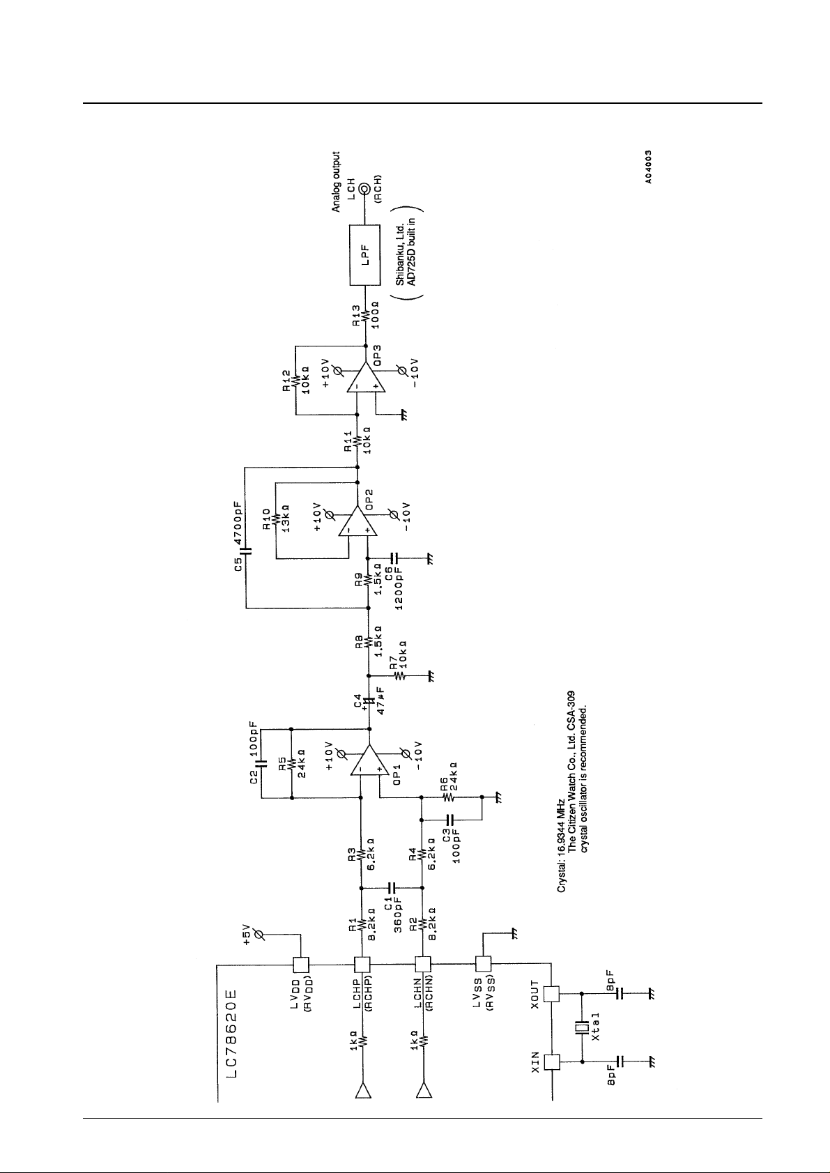
One-Bit D/A Converter Output Block Reference Circuit (normal speed playback)
No. 5130-6/34
LC78620E

Pin Functions
No. 5130-7/34
LC78620E
Pin No. Symbol I/O Function
1 DEFI I Defect detection signal (DEF) input (Must be tied low if unused.)
2 TAI I Test input. A pull-down resistor is built in.
3 PDO O External VCO control phase comparator output
4 VV
SS
PLL pins
Internal VCO ground. Normally 0 V.
5 ISET AI PDO output current adjustment resistor connection
6 VV
DD
Internal VCO power supply. Normally 5 V.
7 FR AI VCO frequency range adjustment
8 V
SS
Digital system ground. Normally 0 V.
9 EFMO O EFM signal inverted output
10 EFMO O Slice level control EFM signal output
11 EFMIN I EFM signal input
12 TEST2 I Test input. A pull-down resistor is built in.
13 CLV
+
O Spindle servo control output. Acceleration when CLV+is high, deceleration when CLV–is high
14 CLV
–
O Three-value output is also possible when specified by microprocessor command.
15 V/P O
Rough servo/phase control automatic switching monitor output. Outputs a high level during rough servo and a low level
during phase control.
16 FOCS O Focus servo on/off output. Focus servo is on when the output is low.
17 FST O Focus start pulse output. This is an open-drain output.
18 FZD I Focus error zero cross signal input. (Must be tied low if unused.)
19 HFL I Track detection signal input. This is a Schmitt input.
20 TES I Tracking error signal input. This is a Schmitt input.
21 PCK O EFM data playback clock monitor. Outputs 4.3218 MHz when the phase is locked.
22 FSEQ O
Synchronization signal detection output. Outputs a high level when the synchronization signal detected from the EFM
signal and the internally generated synchronization signal agree.
23 TOFF O Tracking off output
24 TGL O Tracking gain switching output. Increase the gain when low.
25 THLD O Tracking hold output
26 TEST3 I Test input. A pull-down resistor is built in.
27 V
DD
Digital system power supply. Normally 5 V.
28 JP
+
O
Track jump output. A high level output from JP+indicates acceleration during an outward jump or deceleration during an
inward jump.
29 JP
–
O
A high level output from JP
–
indicates acceleration during an inward jump or deceleration during an outward jump.
Three-value output is also possible when specified by microprocessor command.
30 DEMO I Sound output function input used for end product adjustment manufacturing steps. A pull-down resistor is built in.
31 TEST4 I Test input. A pull-down resistor is built in.
32 EMPH O De-emphasis monitor pin. A high level indicates playback of a de-emphasis disk.
33 LRCKO O Word clock output
34 DFORO O
Digital filter outputs
Right channel data output
35 DFOLO O Left channel data output
36 DACKO O Bit clock output
37 TST10 O Test output. Leave open. (Normally outputs a low level.)
38 ASDACK I Bit clock input
39 ASDFIN I
Antishock system inputs
Left/right channel data input
40 ASDFIR I
(Must be tied low if unused.)
Test input. (Should be tied low for normal operation.)
41 ASLRCK I Word clock input
Continued on next page.

Continued from preceding page.
No. 5130-8/34
LC78620E
Pin No. Symbol I/O Function
42 LRSY O Left/right clock output
43 CK2 O
Bit clock output Inverted polarity clock output
ROMXA application
(after reset) (during CK2CON mode)
44 ROMXA O
output signals
Interpolation data output ROM data output
(after reset) (During ROMXA mode)
45 C2F O C2 flag output
46 MUTEL O Left channel mute output
47 LV
DD
Left channel power supply. Normally 5 V.
48 LCHP O Left channel P output
49 LCHN O Left channel N output
50 LV
SS
One-bit D/A converter
Left channel ground. Normally 0 V.
51 RV
SS
Right channel ground. Normally 0 V.
52 RCHN O Right channel N output
53 RCHP O Right channel P output
54 RV
DD
Right channel power supply. Normally 5 V.
55 MUTER O Right channel mute output
56 DOUT O Digital output
57 SBSY O Subcode block synchronization signal
58 EFLG O C1, C2, single and double error correction monitor pin
59 PW O Subcode P, Q, R, S, T, U, V and W output
60 SFSY O Subcode frame synchronization signal output. This signal falls when the subcodes are in the standby state.
61 SBCK I Subcode readout clock input. This is a Schmitt input. (Must be tied low when unused.)
62 FSX O Output for the 7.35 kHz synchronization signal divided from the crystal oscillator
63 WRQ O Subcode Q output standby output
64 RWC I Read/write control input. This is a Schmitt input.
65 SQOUT O Subcode Q output
66 COIN I Command input from the control microprocessor
67 CQCK I Input for both the command input acquisition clock and the SQOUT pin subcode readout clock input. This is a Schmitt input.
68 RES I Chip reset input. This pin must be set low briefly after power is first applied.
69 TST11 O Test output. Leave open. (Normally outputs a low level.)
70 LASER O Laser on/off output. Controlled by serial data commands from the control microprocessor.
71 16M O 16.9344 MHz output. However, in 4× playback mode only, outputs 33.8688 MHz.
72 4.2M O 4.2336 MHz output
73 CONT O Supplementary control output. Controlled by serial data commands from the control microprocessor.
74 TEST5 I Test input. A pull-down resistor is built in.
75 CS I Chip select input. A pull-down resistor is built in.
76 XV
SS
Crystal oscillator ground. Normally 0 V.
77 X
IN
I
Connections for a 16.9344 MHz crystal oscillator. Use a 33.8688 MHz crystal oscillator in systems that support
78 X
OUT
O
quad-speed playback.
79 XV
DD
Crystal oscillator power supply. Normally 5 V.
80 TEST1 I Test input. A pull-down resistor is built in.
CD System Block Diagrams
Pin Applications
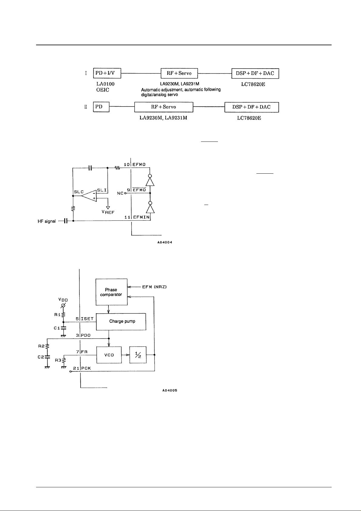
1. HF Signal Input Circuit; Pin 11: EFMIN, pin 10: EFMO, pin 9: EFMO, pin 1: DEFI, pin 13: CLV
+
An EFM signal (NRZ) sliced at an optimal level can be acquired
by inputting the HF signal to EFMIN.
The LC78620E handles defects as follows. When a high level is
input to the DEFI pin (pin 1), the EFMO (pin 9) and EFMO (pin
10) pins (the slice level control outputs) go to the highimpedance state, and the slice level is held. However, note that
this function is only valid in CLV phase control mode, that is,
when the V/P pin (pin 15) is low. This function can be used in
combination with the LA9230M and LA9231M DEF pins.
Note: If the EFMIN and CLV+signal lines are too close to each
other, unwanted radiation can result in error rate
degradation. We recommend laying a ground or V
DD
shield line between these two lines.
2. PLL Clock Generation Circuit; Pin 3: PDO, pin 5: ISET, pin 7: FR, pin 21: PCK
Since the LC78620E includes a VCO circuit, a PLL circuit can
be formed by connecting an external RC circuit. ISET is the
charge pump reference current, PDO is the VCO circuit loop
filter, and FR is a resistor that determines the VCO frequency
range.
(Reference values)
R1 = 68 kΩ, C1 = 0.1 µF
R2 = 680 kΩ, C2 = 0.1 µF
R3 = 5.1 kΩ
Note: We recommend using a ±1.0% tolerance (rank F) carbon
firm resistor for R3.
3. VCO Monitor; Pin 21: PCK
PCK is a monitor pin that outputs an average frequency of 4.3218 MHz, which is divided from the VCO frequency.
4. Synchronization Detection Monitor; Pin 22: FSEQ
Pin 22 goes high when the frame synchronization (a positive polarity synchronization signal) from the EFM signal
read in by PCK and the timing generated by the counter (the interpolation synchronization signal) agree. This pin is
thus a synchronization detection monitor. (It is held high for a single frame.)
No. 5130-9/34
LC78620E
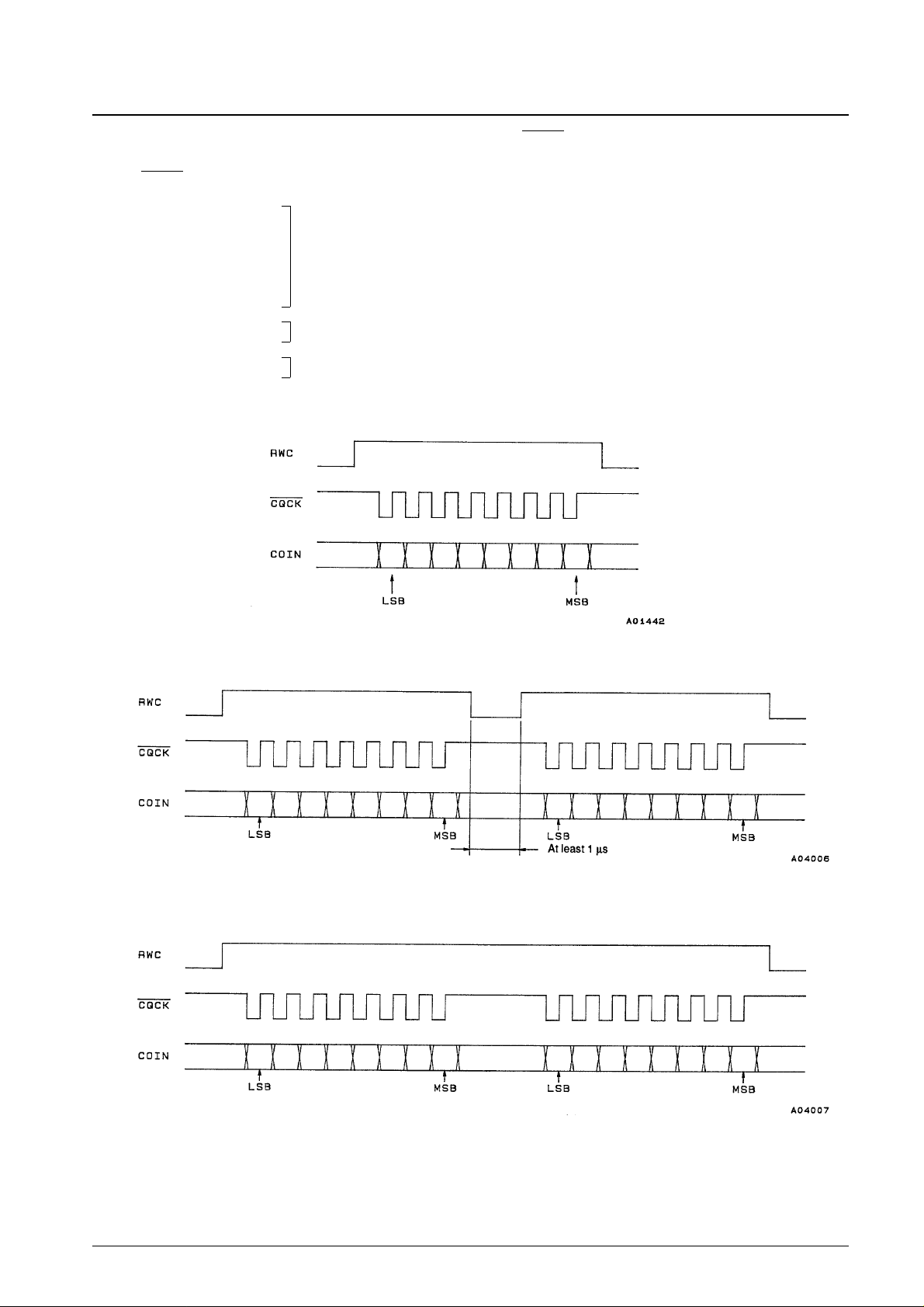
5. Servo Command Function; Pin 64: RWC, pin 66: COIN, pin 67: CQCK
Commands can be executed by setting RWC high and inputting commands to the COIN pin in synchronization with
the CQCK clock. Note that commands are executed on the falling edge of RWC.
Focus start
Track jump
Muting control One-byte commands
Disk motor control
Miscellaneous control
Track check Two-byte command (RWC set twice)
Digital attenuator Two-byte command (RWC set once)
• One-byte commands
• Two-byte commands (RWC set twice)
• Two-byte commands (RWC set once)
No. 5130-10/34
LC78620E
• Command noise rejection
This command reduces the noise on the CQCK clock signal. While this is effective for noise pulses shorter than
500 ns, the CQCK timings T
WøL
, T
WøH
, and t
setup
(see pages 4 and 5, figures 1 and 2), must be set for at least 1 µs.
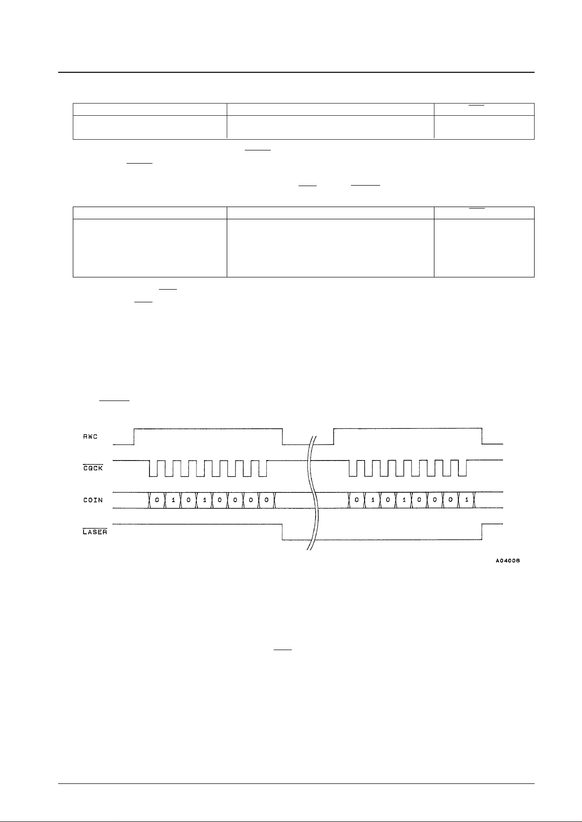
6. Focus Servo Circuit; Pin 16: FOCS, pin 17: FST, pin 18: FZD, pin 70: LASER
The FOCS, FST, and FZD pins are not required when the LC78620E is used in combination with the LA9230M or
the LA9231M. FZD should be tied low when these pins are not used. The LA9230M and LA9231M focus start
command is identical to the LC78620E FOCUS START #1 command.
• NOTHING
This command can be used to initialize the LC78620E by inputting FE (hexadecimal). Note that 00 (hexadecimal)
is the reset command for the LA9230M and the LA9231M, and should be used with care since it clears the result
of the automatic adjustment process and returns these chips to their initial states.
• Laser control
The LASER pin can be use as an extended output port.
• Focus start
When the LC78620E is used in combination with the LA9230M or the LA9231M, the focus start operation is
executed completely on the servo side by commands from the control microprocessor. The following section
describes this operation when the LC78620E is used in combination with the LA9230M or the LA9231M.
When a focus start instruction (either FOCUS START #1 or FOCUS START #2) is input as a servo command,
first the charge on capacitor C1 is discharged by FST and the objective lens is lowered. Next, the capacitor is
charged by FOCS, and the lens is slowly raised. FZD falls when the lens reaches the focus point. When this signal
is received, FOCS is reset and the focus servo turns on. After sending the command, the microprocessor should
check the in-focus detection signal (the LA9210 DRF signal) to confirm focus before proceeding to the next part of
the program. If focus is not achieved by the time C1 is fully charged, the microprocessor should issue another
focus command and iterate the focus servo operation.
No. 5130-11/34
LC78620E
MSB LSB Command RES = low
1 1 1 0 1 1 1 1 COMMAND INPUT NOISE REDUCTION MODE
1 1 1 0 1 1 1 0 RESET NOISE EXCLUSION MODE
●●
MSB LSB Command RES = low
0 0 0 0 1 0 0 0 FOCUS START #1
1 0 1 0 0 0 1 0 FOCUS START #2
0 0 0 0 1 0 1 0 LASER ON
1 0 0 0 1 0 1 0 LASER OFF
●●
1 1 1 1 1 1 1 0 NOTHING
 Loading...