

Page 1

Ordering number : EN6020
D1898RM (OT) No. 6020-1/11
Overview
The LC78601E CMOS IC implements compact disc
player signal processing, servo control, LCD display, key
input acquisition, and remote controller processing
without requiring control by a separate microcontroller.
The basic functions provided include demodulation of the
EFM signal from the optical pickup, deinterleaving, error
detection and correction, 8× oversampling digital filters,
D/A converter (with built-in analog low-pass filter), LCD
driver, remote controller processing, key acquisition, and
control processing. Thus this IC can provide excellent
cost/performance characteristics when implementing a
low-end CD player.
Functions
• Implements CD play/pause, disc stop, track selection,
fast forward, reverse, repeat mode playback of 1 track or
the whole disc, programmed play (setup, play, and clear)
of up to 16 tracks, and random repeat play under the
control of key input or remote controller input.
<Signal-Processing Block>
• Slices an input high-frequency signal at an accurate
level, converts the EFM signal, and generates a clock
with an average frequency of 4.3218 MHz using a PLL
circuit that performs a phase comparison with an
internal VCO.
• Accurately generates not only the reference clock but
also all necessary internal timings using an external
16.9344MHz crystal.
• Controls the disc motor speed using a frame difference
signal created based on the reproduced clock signal and
a reference clock.
• Performs detection, protection, and interpolation for the
frame synchronizing signal to assure stable data readout.
• Demodulates the EFM signal, converting it to 8-bit
symbol data.
• Separates the subcode data from the EFM signal and
outputs that data to the internal control processing block.
• After applying a CRC check to the subcode Q signal,
outputs that signal to the internal control processing
block.
• Buffers the demodulated EFM signal data in internal
RAM and compensates for ±4 frames of jitter due to
disc speed fluctuations.
• Performs unscrambling and deinterleaving by reordering
the demodulated EFM signal data to the stipulated order.
• Performs error detection and correction and flag
processing (C1: dual errors, C2: dual errors)
• The C2 flags are set based on the C1 flags and the result
of the C2 processing, and the signal is interpolated or
previous value hold is applied based on the C2 flags.
Dual interpolation is adopted in the interpolation circuit.
Previous value hold is applied if two or more
consecutive errors are indicated by the C2 flags.
• Performs track jump, focus start, disc motor start/stop,
muting on/off, track count, and other operations under
control of the internal control processing block.
• Provides digital outputs.
• Generates D/A converter input signals with continuity
improved by 8× oversampling digital filters.
• Includes on-chip third-order noise shaper delta-sigma
D/A converters with built-in analog low-pass filter.
• Digital deemphasis circuit
• Adopts zero-cross muting.
<Display Block>
• On-chip LCD drivers for 2-digit display plus play,
program, repeat, and random indicators
• On-chip bias voltage generator
<Control Processing Block>
• Key matrix circuit with 4 inputs and 2 outputs for an
8-key matrix
• Supports remote controller input.
LC78601E
SANYO Electric Co.,Ltd. Semiconductor Bussiness Headquarters
TOKYO OFFICE Tokyo Bldg., 1-10, 1 Chome, Ueno, Taito-ku, TOKYO, 110-8534 JAPAN
Compact Disc Player DSP with
Built-in Microcontroller
CMOS IC
Any and all SANYO products described or contained herein do not have specifications that can handle
applications that require extremely high levels of reliability, such as life-support systems, aircraft’s
control systems, or other applications whose failure can be reasonably expected to result in serious
physical and/or material damage. Consult with your SANYO representative nearest you before using
any SANYO products described or contained herein in such applications.
SANYO assumes no responsibility for equipment failures that result from using products at values that
exceed, even momentarily, rated values (such as maximum ratings, operating condition ranges, or other
parameters) listed in products specifications of any and all SANYO products described or contained
herein.
Page 2
Features
• Package: 64-pin QFP
• 5-V single-voltage power supply
No. 6020-2/11
LC78601E
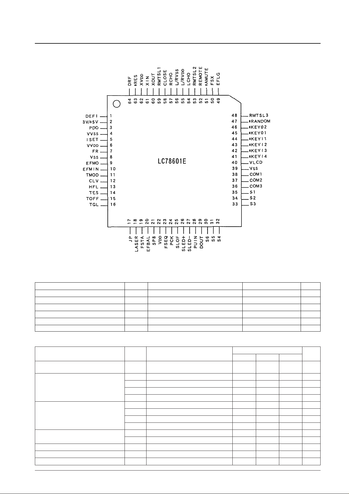
Equivalent Circuit Block Diagram
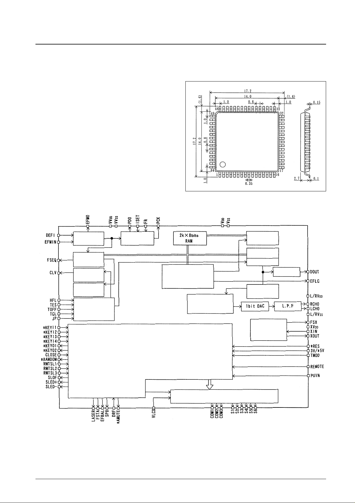
Package Dimensions
unit: mm
3159-QFP64E
SANYO: QFP64E(QIP64E)
[LC78601E]
Slice level
control
VCO clock
oscillator
Clock control
Synchronization
detection
EFM demodulation
CLV digital
servo
Subcode
separator QCRC
Servo commander
C1 and C2 error detection
and correction
Flag processing
RAM address
generator
Interpolation
and muting
Bilingual support circuit
8 × oversampling
digital filters
Digital output circuit
Digital
attenuator
Crystal oscillator
circuit
Timing generator
System control
LCD driver
Page 3
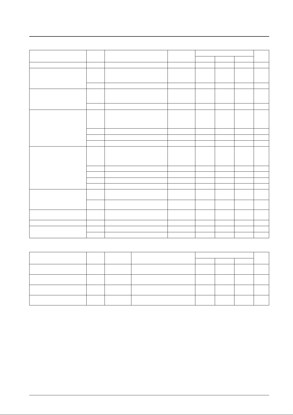
Pin Assignment
No. 6020-3/11
LC78601E
Parameter Symbol Conditions Ratings Unit
Maximum supply voltage V
DD
max VSS– 0.3 to VSS+ 7.0 V
Input voltage V
IN
VSS– 0.3 to VSS+ 0.3 V
Output voltage V
OUT
VSS– 0.3 to VSS+ 0.3 V
Allowable power dissipation Pd max 300 mW
Operating temperature Topr –20 to +75 °C
Storage temperature Tstg –40 to +125 °C
Specifications
Absolute Maximum Ratings at Ta = 25°C, VSS= 0 V
Parameter Symbol Conditions
Ratings
Unit
min typ max
Supply voltage V
DD
VDD, XVDD, L/RVDD, VV
DD
4.5 5.5 V
Normal speed playback
V
IH
1 DEFI, 3 V/*5 V, TMOD, *RES, HFL, TES 0.7 V
DD
V
DD
V
High-level input voltage
V
IH
2 *KEYI1 to 4 0.8 V
DD
V
DD
V
V
IH
3 EFMIN 0.6 V
DD
V
DD
V
V
IH
4 PUIN, RMTSL1 to 3, REMOTE, CLOSE, DRF 0.8 V
DD
V
DD
V
V
IL
1 DEFI, 3 V/*5 V, TMOD, *RES, HFL, TES 0 0.3 V
DD
V
Low-level input voltage
V
IL
2 *KEYI1 to 4 0 0.5 V
DD
V
V
IL
3 EFMIN 0 0.4 V
DD
V
V
IL
4 PUIN, RMTSL1 to 3, REMOTE, CLOSE, DRF 0 0.2 V
DD
V
Input level
V
IN
1 EFMIN: Slice level control 1.0 Vp-p
V
IN
2 XIN: Capacitor coupled input 1.0 Vp-p
Operating frequency range f
OP
EFMIN 10 MHz
Crystal oscillator frequency fX X
IN
, X
OUT
16.9344 MHz
Input voltage V
LCD1
0.5 V
DD
V
DD
V
Allowable Operating Ranges at Ta = –20 to +75°C, VDD= 4.5 to 5.5 V, VSS= 0 V
Top view
Page 4
No. 6020-4/11
LC78601E
Parameter Symbol Applicable pins Conditions
Ratings
Unit
min typ max
Current drain I
DD
VDD, XVDD, L/RVDD, VV
DD
35 55 mA
DEFI, 3 V/*5 V, EFMIN, TMOD, HFL,
High-level input current
IIH1 TES, PUIN, *KEYI1 to 4, RMTSL1 to 3, VIN= V
DD
5 µA
REMOTE, CLOSE, *RES, DRF
IIH2 LASER, FSTA, EFBAL, SP8 VIN= V
DD
250 500 1000 µA
DEFI, 3 V/*5 V, EFMIN, TMOD, HFL,
Low-level input current
IIL1 TES, RMTSL2 to 3, REMOTE, *RES, VIN= 0 V –5 µA
DRF
IIL2 PUIN, *KEYI1 to 4, RMTSL1, CLOSE VIN= 0 V –25 –50 –100 µA
EFMO, CLV, TOFF, TGL, JP, LASER,
V
OH
1
FSTA, EFBAL, SP8, FSEQ, PCK,
IOH= –1 mA 0.8 V
DD
V
SLOF, SLED+, SLED–, EFLG, FSX,
High-level output voltage
*AMUTE
V
OH
2 S1 to 6 IOH= –0.02 mA 0.8 V
DD
V
V
OH
3 COM1 to 3 IOH= – 0.1 mA 0.8 V
DD
V
V
OH
4 DOUT IOH= –12 mA 0.9 V
DD
V
EFMO, CLV, TOFF, TGL, JP, FSEQ,
V
OL
1
PCK, SLOF, SLED+, SLED–,
IOL= 1 mA 0.2 V
DD
V
*KEYO1 to 2, EFLG, FSX,
RMTSL2 to 3, *AMUTE
Low-level output voltage VOL2 *RANDOM IOL= 8 mA 0.2 V
DD
V
V
OL
3 S1 to 6 IOL= 0.02 mA 0.2 V
DD
V
V
OL
4 COM1 to 3 IOL= 0.1 mA 0.2 V
DD
V
V
OL
5 DOUT IOL= 12 mA 0.1 V
DD
V
I
OFFH
PDO, CLV, JP, *KEY01 to 2,
V
OUT
= V
DD
5 µA
Output off leakage current
*RANDOM
I
OFFL
PDO, CLV, JP, *KEY01 to 2,
V
OUT
= 0 V –5 µA
*RANDOM
Pull-up resistance R
PU
PUIN, *KEYI1 to 4, RMTSL1, CLOSE,
100 kΩ
*RES
Pull-down resistance R
PD
LASER, FSTA, EFBAL, SP8 10 kΩ
Charge pump output current
I
PDOH
PDO R
ISET
= 68 kΩ 64 80 96 µA
I
PDOL
PDO R
ISET
= 68 kΩ –96 –80 –64 µA
Electrical Characteristics at Ta = –20 to +75°C, VDD= 4.5 to 5.5 V, VSS= 0 V
Parameter Symbol Applicable pins Conditions
Ratings
Unit
min typ max
Total harmonic distortion THD+N LCHO, RCHO
1 kHz: 0dB data input
0.02 0.035 %
20kHz low-pass filter used (built-in AD725D)
Dynamic range DR LCHO, RCHO
1 kHz: –60dB data input
86 88 dB
20kHz low-pass filter and A filter used (built-in AD725D)
Signal-to-noise ratio S/N LCHO, RCHO
1 kHz: 0dB data input
96 98 dB
20kHz low-pass filter and A filter used (built-in AD725D)
Crosstalk CT LCHO, RCHO
1 kHz: 0dB data input
80 82 dB
20kHz low-pass filter used (built-in AD725D)
1-Bit D/A Converter Analog Characteristics at Ta = 25°C, VDD= L/RVDD= 5 V, VSS= L/RVSS= 0 V
Note: Measure in normal speed playback mode with the Sanyo 1-bit D/A converter block reference circuit.
Page 5

1-Bit D/A Converter Output Block Reference Circuit
No. 6020-5/11
LC78601E
Oscillator element: 16.9344 MHz
The following oscillator elements are recommended
CSA-309 <C = 8 pF> (Citizen Watch Co., Ltd.)
CSA16.93MXZ040 (C = 15 pF) (Murata Mfg. Co., Ltd.)
CSA16.93MXZ0C3 (built-in capacitor)
(Murata Mfg. Co., Ltd.)
Oscillator
element
AD725D
(Manufactured by
Shibasoku Ltd.)
Analog output
Left channel
(right channel)
Page 6

No. 6020-6/11
LC78601E
Pin Functions
Pin No. Pin I/O Function Pin state during reset
1 DEFI I Defect detection signal (DEF) input. (Must be connected to 0 V if unused.) —
2 3 V/*5 V I Supply voltage selection input. (High: 3V operation, low: 5V operation) —
3 PDO O Internal VCO control phase comparator output Undefined
4 VV
SS
— Internal VCO ground. This pin must be connected to 0 V. —
5 ISET AI PLL circuit pins PDO output current adjustment resistor connection —
6 VV
DD
— Internal VCO power supply —
7 FR AI VCO frequency range adjustment —
8 V
SS
— Digital system ground. This pin must be connected to 0 V. —
9 EFMO O
Slice level
EFM signal output Undefined
10 EFMIN I
control pins
EFM signal input —
11 TMOD I Test input. This pin must be connected to 0 V. —
12 CLV O Disc motor control output. This is a 3-value output. Hi-Z
13 HFL I Track detection signal input. This is a Schmitt input. —
14 TES I Tracking error signal input. This is a Schmitt input. —
15 TOFF O Tracking off output High output
16 TGL O Tracking gain switching output. A low level output raises the gain. Undefined
17 JP O Track jump control output. This is a 3-value output. Hi-Z
18 LASER O Laser control. A pull-down resistor is built in. Pulled down
19 FSTA O FSTA control. A pull-down resistor is built in. Pulled down
20 EFBAL O EFBAL control. A pull-down resistor is built in. Pulled down
21 SP8 O SP8 control. A pull-down resistor is built in. Pulled down
22 V
DD
— Digital system power supply —
23 FSEQ O
Synchronizing signal detection output. Outputs a high level if the synchronizing signal detected
Undefined
from the EFM signal and the internally generated synchronizing signal match.
EFM data playback clock monitor. 4.3218 MHz when the phase is locked.
24 PCK O (Note that this output is only provided in test mode. This pin outputs a low level during normal Low output
mode operation.)
25 SLOF O Sled off control output High output
26 SLED+ O
Sled feed output
Low output
27 SLED– O Low output
28 PUIN I Limit switch detection input —
29 DOUT O Digital output (EIAJ format) Undefined
30 S6 O Segment output (6) Low output
31 S5 O Segment output (5) Low output
32 S4 O Segment output (4) Low output
33 S3 O Segment output (3) Low output
34 S2 O Segment output (2) Low output
35 S1 O Segment output (1) Low output
36 COM3 O Common driver output (3) Low output
37 COM2 O Common driver output (2) Low output
38 COM1 O Common driver output (1) Low output
39 V
SS
— Digital system ground. This pin must be connected to 0 V. —
40 VLCD1 — LCD drive bias 1/2 V
DD
monitor —
41 *KEYI4 I Key matrix input (4). A pull-up resistor is built in. —
42 *KEYI3 I Key matrix input (3). A pull-up resistor is built in. —
43 *KEYI2 I Key matrix input (2). A pull-up resistor is built in. —
44 *KEYI1 I Key matrix input (1). A pull-up resistor is built in. —
45 *KEYO1 O Key matrix common output (1). This is an open-drain output. Hi-Z
46 *KEYO2 O Key matrix common output (2). This is an open-drain output. Hi-Z
47 *RANDOM O Random mode indicator output (Low: random mode, high: modes other than random mode.) Hi-Z
Remote controller identifier input (3). This pin functions as an output pin set to the low level
48 RMTSL3 I/O
during resets (when the *RES pin is low) and for a few milliseconds after the *RES pin
Low output
switches to the high level. Therefore, applications that will set this pin high must connect an
external pull-up resistor to this pin.
Continued on next page.
Page 7

No. 6020-7/11
LC78601E
Pin No. Pin I/O Function Pin state during reset
Monitor for C1, C2, single, and double error corrections.
49 EFLG O (Note that this output is only provided in test mode. This pin outputs a low level during normal Low output
mode operation.)
Outputs a 7.35 kHz synchronizing signal that is generated by dividing the crystal oscillator output.
50 FSX O (Note that this output is only provided in test mode. This pin outputs a low level during normal Low output
mode operation.)
51 *AMUTE O Audio mute output signal Low output
52 REMOTE I Remote controller signal input —
Remote controller identifier input (2). This pin functions as an output pin set to the low level
53 RMTSL2 I/O
during resets (when the *RES pin is low) and for a few milliseconds after the *RES pin
Low output
switches to the high level. Therefore, applications that will set this pin high must connect an
external pull-up resistor to this pin.
54 LCHO O Left channel D/A converter output Undefined
55 L/RV
DD
— D/A converter power supply —
56 L/RV
SS
— D/A converter ground. This pin must be connected to 0 V. —
57 RCHO O Right channel D/A converter output Undefined
58 CLOSE I Close switch detection input. A pull-up resistor is built in. —
59 RMTSL1 I Remote controller identifier input (1). A pull-up resistor is built in. —
60 X
OUT
O
Connections for a 16.9344 crystal element
Clock output
61 X
IN
I —
62 XV
DD
— Crystal oscillator circuit power supply —
63 *RES I IC reset input. Applications must set this pin low temporarily when power is first applied. —
64 DRF I DRF input. (Connected when an LA9250M is used.) —
Continued from preceding page.
Note: The same potential must be connected to all the power supply pins (VDD, VVDD, L/RVDD, and XVDD).
Page 8

Sample Application Circuit
Note: This circuit is an example of typical connections used with the LC78601E, but is not a complete circuit, i.e. certain peripheral components and circuits have been omitted.
Contact your Sanyo representative for detailed information on this circuit.
No. 6020-8/11
LC78601E
Page 9

Notes on Application Design
It goes without saying that applications must strictly observe the absolute maximum ratings and allowable operating
ranges (and recommended operating conditions) stipulated for this IC to achieve reliability as a system. However, we
also strongly recommend that designers carefully consider both the mounting conditions and the actual usage
environment, including ambient temperatures and static electricity, when designing applications.
This section provides additional notes concerning design, mounting, and certain other points that require care during
application design.
1. Handling of Unused Pins
If any unused pins on this IC are left in the open state, certain internal states may become undefined. Unused pins for
which the handling is specified in the documentation must be handled as specified. Also be sure that no output pins
contact any power supply or ground lines or any other output pin.
2. Latch-up Prevention
• Due to the internal structure of this IC, the same potential must be applied to all power supply pins.
— Also provide the same potential to the servo system ASP. Since the slice level control circuit is shared with this IC,
the same power supply potential must be applied. Also be sure to apply the same potential to all ASP power supply
pins.
— For products in which the power supply pins are completely isolated within the IC and special allowances apply, be
sure to follow the detailed instructions in the documentation.
• The IC may latch up if timing discrepancies appear between the rise times for different power supply pins. Design
applications so that no discrepancies appear.
• Do not raise the voltage of any input or output pin above the VDDlevel, and do not lower the voltage below VSS. This
point requires special care when power is first applied.
• Do not allow overvoltages or abnormal signal noise levels to be applied to this IC.
• In general, latch-up can be prevented by tying unused input pins to VDDor VSS. However, the directions for unused pin
handling in the documentation for this IC must be followed.
• Do not short the outputs.
3. Interface
When different devices are connected, incorrect operation may result if the input VILand VIHand the output VOLand
VOHlevels do not match. Insert level shifters so that the IC is not destroyed if it is connected to a device that uses a
different power-supply voltage, such as in a dual power supply system applications.
4. Load Capacitance and Output Current
• If a load with a large capacitance is connected, the wiring may fuse since such a load can result in the equivalent of an
output short for an extended period. Also, excessive charge and discharge currents can cause noise and degrade
application performance or lead to incorrect operation. Use loads of the recommended capacitance.
• Excessive output sink or source currents can lead to problems similar to those described above. Use this IC within the
recommended current levels while taking the maximum allowable power dissipation into consideration as well.
5. Notes on Power Application and Reset
• There are cases where care is required at power on, during a reset, and when the reset state is cleared. Refer to the
specifications sheet for the product and observe the notes concerning power on and IC reset.
• The pin output states, the pin I/O direction settings, and the contents of the registers are not guaranteed when power is
first applied in this IC. Items that are defined by the reset operation and when the mode is set are guaranteed after that
operation. Applications must first apply a reset to this IC after power is applied. Since pin states and register contents
that are not defined by the reset operation may change over time from the states in early versions due to long term
variations across lots, applications should not depend on these values.
No. 6020-9/11
LC78601E
Page 10

6. Notes on Thermal Design
The failure rate of semiconductor devices is accelerated by higher ambient temperatures and power dissipation levels.
We strongly recommend taking changes in ambient conditions into account and providing as large a margin as
possible in thermal design to assure high reliability.
7. Notes on Printed Circuit Board Pattern Design
• Ideally, the influence of shared impedances should be minimized by separating the VDDand ground lines for each
system.
• Design VDDand ground lines to be as short and as wide as possible, and to have the lowest high-frequency impedance
possible. Ideally, decoupling capacitors (0.01 to 1 µ F) should be inserted in each VDD/ground pair. These capacitor
should be placed as close to the corresponding VDDpin as possible. It is also appropriate to insert capacitors of about
100 to 220 µ F between each VDDand ground as low-frequency filters. However, be careful not to use values that are
too large for these capacitors, since that can result in latch-up.
— In the servo system, the reference voltage line (V
REF
) and the driver VCCand ground lines are handled in the same
way. The driver ground line should be made especially wide. If at all possible, use the recommended driver pattern,
which, being directly under the device, was also designed to provide a heat dissipation effect as well.
— If a current output pickup is used, locate the optical pickup element connector and the ASP RF input as close
together as possible. Even if a voltage output type pickup is used, the I/V conversion resistor located at the ASP
input should be located near the ASP RF input.
• The EFM signal line should be made as short as possible, and should either be located away from adjacent lines or
should be shielded from adjacent lines by VSSor VDDshield lines.
Since the slice level control output (EFMO) can easily disrupt the EFM signal line, the resistor connected to the output
pin should be located as close to the pin as possible. Note that reducing the value of this resistor increases the influence
of spurious radiation and cares must be taken for the output level when the value increases.
• Cover the area around the crystal with the ground pattern.
8. Other Notes
If you have any questions during the application design phase, do not hesitate to contact your Sanyo sales
representative or the nearest Sanyo semiconductor sales office.
This IC is specifically designed for use in CD players, and as such its specifications differ from those of generalpurpose product standard logic ICs. We recommend system debugging using the end product system itself and
adopting failsafe system design if required by the application.
No. 6020-10/11
LC78601E
Page 11

PS No. 6020-11/11
LC78601E
This catalog provides information as of December, 1998. Specifications and information herein are
subject to change without notice.
Specifications of any and all SANYO products described or contained herein stipulate the performance,
characteristics, and functions of the described products in the independent state, and are not guarantees
of the performance, characteristics, and functions of the described products as mounted in the customer’s
products or equipment. To verify symptoms and states that cannot be evaluated in an independent device,
the customer should always evaluate and test devices mounted in the customer’s products or equipment.
SANYO Electric Co., Ltd. strives to supply high-quality high-reliability products. However, any and all
semiconductor products fail with some probability. It is possible that these probabilistic failures could
give rise to accidents or events that could endanger human lives, that could give rise to smoke or fire,
or that could cause damage to other property. When designing equipment, adopt safety measures so
that these kinds of accidents or events cannot occur. Such measures include but are not limited to protective
circuits and error prevention circuits for safe design, redundant design, and structural design.
In the event that any or all SANYO products (including technical data, services) described or contained
herein are controlled under any of applicable local export control laws and regulations, such products must
not be exported without obtaining the export license from the authorities concerned in accordance with the
above law.
No part of this publication may be reproduced or transmitted in any form or by any means, electronic or
mechanical, including photocopying and recording, or any information storage or retrieval system,
or otherwise, without the prior written permission of SANYO Electric Co., Ltd.
Any and all information described or contained herein are subject to change without notice due to
product/technology improvement, etc. When designing equipment, refer to the “Delivery Specification”
for the SANYO product that you intend to use.
Information (including circuit diagrams and circuit parameters) herein is for example only; it is not
guaranteed for volume production. SANYO believes information herein is accurate and reliable, but
no guarantees are made or implied regarding its use or any infringements of intellectual property rights
or other rights of third parties.
 Loading...