

Page 1
Any and all SANYO products described or contained herein do not have specifications that can handle
applications that require extremely high levels of reliability, such as life-support systems, aircraft’s
control systems, or other applications whose failure can be reasonably expected to result in serious
physical and/or material damage. Consult with your SANYO representative nearest you before using
any SANYO products described or contained herein in such applications.
SANYO assumes no responsibility for equipment failures that result from using products at values that
exceed, even momentarily, rated values (such as maximum ratings, operating condition ranges,or other
parameters) listed in products specifications of any and all SANYO products described or contained
herein.
CMOS IC
Analog Function Switch
Ordering number:ENN3641
LC7824
SANYO Electric Co.,Ltd. Semiconductor Company
TOKYO OFFICE Tokyo Bldg., 1-10, 1 Chome, Ueno, Taito-ku, TOKYO, 110-8534 JAPAN
Overview
The LC7824 is an analog switch incorporating seven
switches into a single chip, making it ideal for audio and
video applications in amplifiers, receivers and television
equipment.
The LC7824 is controlled from a three-wire bus (C
lowing for an easy interface with a microcontroller. In addition, a device select pin allows two devices to be connected to the bus.
The LC7824 operates from a ±9V supply and is available
in 16-pin DIPs.
2
B), al-
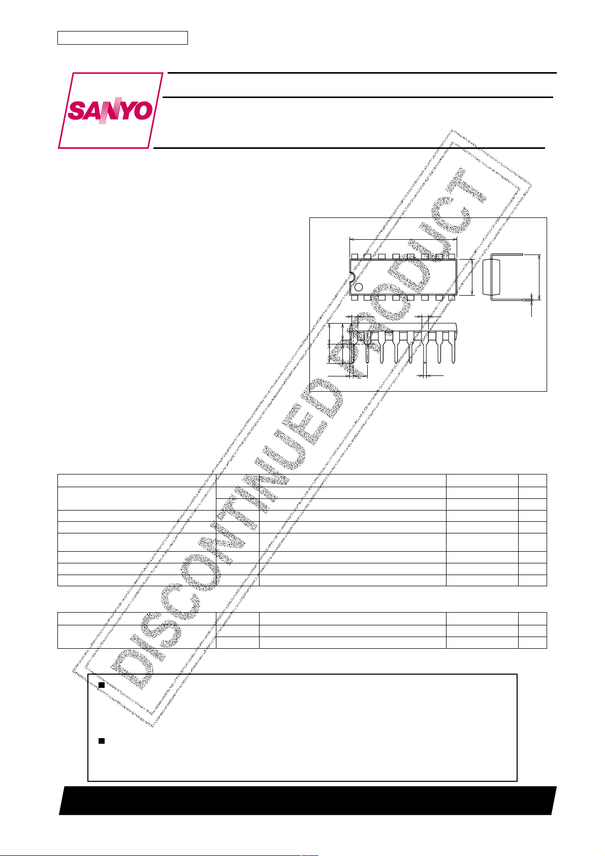
Package Dimensions
unit:mm
3006C-DIP16
[LC7824]
19.0
16
1
1.09
9
6.4
8
1.2
7.62
0.25
Features
• Audio and video bandwidth.
• Seven analog switches.
• Select pin allows two LC7824s to be connected to a common, serial data bus.
• Easy microcontroller interface.
• ±9V supply.
• 16-pin DIP.
Specifications
Absolute Maximum Ratings
retemaraPlobmySsnoitidnoCsgnitaRtinU
V
xam 01+ot3.0–V
egatlovylppusmumixaM
egnaregatlovtupnilevel-cigoLV
egnaregatlovtupnihctiwsgolanAV
desolc
noitapissidrewopelbawollAxamdP 001Wm
egnarerutarepmetgnitarepOrpoT 57+ot03–
egnarerutarepmetegarotSgtsT 521+ot04–
nehwsehctiwsssorcalaitnereffidegatloV
Recommended Operating Conditions at Ta = 25˚C
retemaraPlobmySsnoitidnoCsgnitaRtinU
egatlovylppuS
DD
V
xam 3.0+ot01–V
EE
1I
2I
∆V
NO
V
DD
V
EE
3.65max
3.4
(0.61)
(3.0)
0.51min
2.54
0.48
V
EE
SANYO : DIP16
01+ot3.0–V
Vot3.0–
3.0+
DD
5.0V
9ot5.4V
0ot9–V
V
˚C
˚C
51501TN (KT)/O050JN No.3641–1/4
Page 2
LC7824
Electrical Characteristics at Ta = –30 to +75˚C, VDD=4.5 to 9V
retemaraPlobmySsnoitidnoC
tnerrucylppuSI
2
C
2
C
dnabssaPf
hguorhtdeeFF
klatssorCC
2
C
egatlovlevel-woltupniBV
egatlovlevel-hgihtupniBV
egatlovlevel-woltupniniptceleSV
egatlovlevel-hgihtupniniptceleSV
ecnatsiserNOhctiwsgolanAR
noitrotsidcinomrahredrodrihtdnadnoceS3H,2HVNIzHM5=f,V1=06Bd
noitrotsidcinomrahlatoTDHT
tnerruclevel-woltupnII
tnerruclevel-hgihtupnII
tnerrucegakaelhctiwSI
egatlovtupnihctiwsgolanAV
htdiwsiseretsyhtupniBV
V
DD
1LI
1HI
2LI
2HI
V
NO
V
V
T
V
V
V
V
HT
V
T
V
LI
V
HI
V
FFO
NI
H
V,V9=
DD
DD
DD
NI
NI
NI
NI
NI
NI
DD
DD
DD
V9–=1Am
EE
V,V5=
V5–=051
EE
V,V9=
V9–=011
EE
nwodBd1–,V1=05zHM
nwodBd3–,V1=001zHM
zHk1=f,V1=10.0%
zHk1=f,V1.0=50.0%
zHM5=f,V1=05Bd
zHM5=f,V1=05Bd
V,V9=
V,V9=
V,V9=
V,V9–=
EE
I
V,V9–=
EE
I
V,V9–=
EE
I
sgnitaR
nimpytxam
V
SS
2.49V
V
SS
V7.0
DD
V0=01– Aµ
V9=01Aµ
V9+ot9–=01– 01+Aµ
V
EE
3.0V
1V
V3.0
DD
V
DD
V
DD
tinU
V
V
Ω
Ω
V
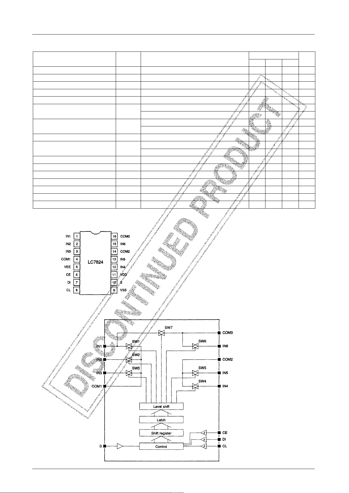
Pin Assignment
Block Diagram
Top view
No.3641–2/4
Page 3

Pin Description
rebmuNemaNnoitpircseD
51,31,21,3,2,16NIot1NIstuptuo/stupnihctiwsgolanA
61,41,43MOCot1MOCstuptuo/stupninommochctiwsgolanA
5V
6ECelbanepihc,reggirt-ttimhcS
7IDtupniatadlaires,reggirt-ttimhcS
8LCtupnikcolc,reggirt-ttimhcS
9VSSdnuorG
01S tupnitceleseciveD
11V
Timing Characteristics
LC7824
EE
DD
egatlovylppusV9–ot5.4–
egatlovylppusV9ot5.4
Ta = –30 to +75˚C, V
emitputeSt
=4.5 to 9V
DD
retemaraPlobmySsnoitidnoC
htdiweslupkcolclevel-WOLt
htdiweslupkcolclevel-HGIHt
gnimittupniatadlaireS
Lo
Ho
putes
t
1
t
2
t
3
sgnitaR
nimpytxam
5.0sµ
5.0sµ
5.0sµ
0sµ
5.0sµ
5.0sµ
Functional Description
The LC7824 analog switch is controlled from a three-wire bus, which comprises chip-enable, clock and serial data
inputs. The 16-bit serial input code comprises eight address bits and eight control bits as shown in figure 1.
Figure 1. Data input
The address data is latched on the rising edge of CE, and the input data, on the falling edge as shown in figure 2.
tinU
Figure 2. Input timing
When S (pin 10) is LOW, the device address is 01101110 (6EH), and when HIGH, 01101111 (6FH).
Each switch is turned ON if the corresponding control bit is 1, and OFF, if 0. The X bit is ignored.
No.3641–3/4
Page 4

T ypical Applications
LC7824
Figure 3. Video switching (1)
Figure 4. Video switching (2)
Specifications of any and all SANYO products described or contained herein stipulate the performance,
characteristics, and functions of the described products in the independent state, and are not guarantees
of the performance, characteristics, and functions of the described products as mounted in the customer's
products or equipment. To verify symptoms and states that cannot be evaluated in an independent device,
the customer should always evaluate and test devices mounted in the customer's products or equipment.
SANYO Electric Co., Ltd. strives to supply high-quality high-reliability products. However, any and all
semiconductor products fail with some probability. It is possible that these probabilistic failures could
give rise to accidents or events that could endanger human lives, that could give rise to smoke or fire,
or that could cause damage to other property. When designing equipment, adopt safety measures so
that these kinds of accidents or events cannot occur. Such measures include but are not limited to protective
circuits and error prevention circuits for safe design, redundant design, and structural design.
In the event that any or all SANYO products(including technical data,services) described or
contained herein are controlled under any of applicable local export control laws and regulations,
such products must not be exported without obtaining the export license from the authorities
concerned in accordance with the above law.
No part of this publication may be reproduced or transmitted in any form or by any means, electronic or
mechanical, including photocopying and recording, or any information storage or retrieval system,
or otherwise, without the prior written permission of SANYO Electric Co. , Ltd.
Any and all information described or contained herein are subject to change without notice due to
product/technology improvement, etc. When designing equipment, refer to the "Delivery Specification"
for the SANYO product that you intend to use.
Information (including circuit diagrams and circuit parameters) herein is for example only ; it is not
guaranteed for volume production. SANYO believes information herein is accurate and reliable, but
no guarantees are made or implied regarding its use or any infringements of intellectual property rights
or other rights of third parties.
This catalog provides information as of May, 2001. Specifications and information herein are subject to
change without notice.
PS No.3641–4/4
 Loading...