

Page 1
Any and all SANYO products described or contained herein do not have specifications that can handle
applications that require extremely high levels of reliability, such as life-support systems, aircraft’s
control systems, or other applications whose failure can be reasonably expected to result in serious
physical and/or material damage. Consult with your SANYO representative nearest you before using
any SANYO products described or contained herein in such applications.
SANYO assumes no responsibility for equipment failures that result from using products at values that
exceed, even momentarily, rated values (such as maximum ratings, operating condition ranges,or other
parameters) listed in products specifications of any and all SANYO products described or contained
herein.
CMOS IC
1/3 Duty General Purpose LCD Drivers
Ordering number:ENN4467
LC75850E, 75850W
SANYO Electric Co.,Ltd. Semiconductor Company
TOKYO OFFICE Tokyo Bldg., 1-10, 1 Chome, Ueno, Taito-ku, TOKYO, 110-8534 JAPAN
Overview
The LC75850E and LC75850W are general purpose LCD
drivers for use in microprocessor controlled applications
such as radio tuner frequency displays.
Functions
• Supports both 1/3 duty 1/2 bias and 1/3 duty 1/3 bias
LCD driver techniques for a maximum of 156 segments.
• Power saving mode allows the backup function to be
switched on or off and all segments to be turned off unconditionally.
• Can be controlled by three serial data lines (CE, CL, and
DI) from the microprocessor. (CCB handling)
• High generality, since se gment data can be displayed without going through a decoder.
• The INH pin unconditionally turns off display.
• The LCD drive bias voltage can be provided internally or
externally .
• Power supply voltage: 4.5 to 8V.
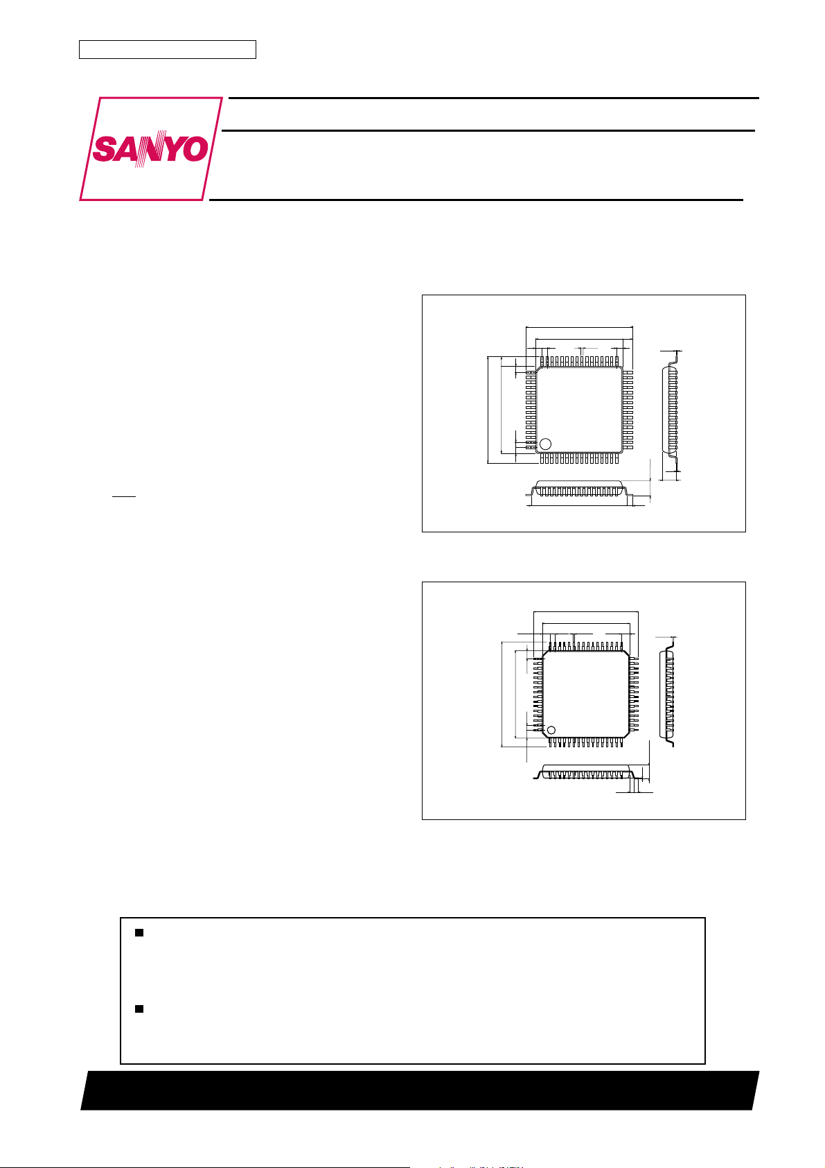
Package Dimensions
unit:mm
3159-QIP64E
[LC75850E]
17.2
14.0
0.8
0.35
15.6
[LC75850W]
12.0
10.0
1.6
17.2
unit:mm
3190-SQFP64
1.0
48
1.0
49
14.0
0.8
64
1.0
1
1.25 0.5 1.250.18
48
49
1.25
1.6
1.0
33
32
17
16
3.0max
0.8
SANYO : QIP64E
33
32
0.15
0.15
0.1
2.7
10.0
12.0
0.5
64
116
1.25
62501TN (KT)/D2493JN B8-0082, 0203 No.4467–1/11
17
1.7max
0.1
0.5
0.5
SANYO : SQFP64
Page 2
LC75850E, 75850W
Specifications
Absolute Maximum Ratings at Ta = 25˚C, VSS = 0V
retemaraPlobmySsnoitidnoCsgnitaRtinU
egatlovylppusmumixaMV
egatlovtupnI
egatlovtuptuOV
tnerructuptuO
noitapissidrewopelbawollAxamdPaT ≤ 58°C 002Wm
erutarepmetgnitarepOrpoT –58+ot04
erutarepmetegarotSgtsT –521+ot55
Allowable Operating Ranges at Ta = –40 to +85˚C, VSS = 0V
retemaraPlobmySsnoitidnoC
egatlovylppuSV
egatlovtupnI
egatlovlevelhgihtupnIV
egatlovlevelwoltupnIV
ecnatsiserlanretxedednemmoceRR
ecnaticapaclanretxedednemmoceRC
egnarrotallicsodeetnarauGf
emitputesataDt
emitdlohataDt
emittiawECt
emitputesECt
emitdlohECt
emitlevelhgihLCt
emitlevelwolLCt
emitesiRt
emitllaFt
emitgnihctiwsHNI2t3erugiF01sµ
xamV
DD
DD
VNI1HNI,ID,LC,EC–0.9+ot3.0V
VNI2CSO–ot3.0VDD3.0+V
CSO–ot3.0VDD3.0+V
TUO
I
125Sot1S 003Aµ
TUO
I
23MOCot1MOC 3Am
TUO
V
DD
DD
VDD1VDD13/2V
VDD2VDD23/1V
HNI,ID,LC,EC0.40.8V
HNI,ID,LC,EC07.0V
2erugiF:ID,LC001sn
2erugiF:ID,LC001sn
2erugiF:LC,EC001sn
2erugiF:LC,EC001sn
2erugiF:LC,EC001sn
2erugiF:LC001sn
2erugiF:LC001sn
2erugiF:ID,LC,EC001sn
2erugiF:ID,LC,EC001sn
øH
øL
HI
LI
CSO74kΩ
CSO
CSO0001Fp
CSO
CSO
CSO918367zHk
sd
hd
pc
sc
hc
r
f
–0.9+ot3.0V
˚C
˚C
sgnitaR
nimpytxam
5.40.8V
DD
DD
0.8V
0.8V
tinU
Electrical Characteristics at Ta = –40 to +85˚C, VSS = 0V
retemaraPlobmySsnoitidnoC
tnerruclevelhgihtupnII
tnerruclevelwoltupnII
ycneuqerfrotallicsOf
siseretsyHV
egatlovlevelhgihtuptuOV
egatlovlevelwoltuptuOV
egatlovlevelhgihtuptuOV
egatlovlevelwoltuptuOV
*egatlovleveletaidemretnI
V
V
V
V
V
1V;HNIID,LC,EC
HI
2V;HNIID,LC,EC
LI
CSO
H
1I;25Sot1S
HO
1I;25Sot1S
LO
2I;3MOCot1MOC
HO
2I;3MOCot1MOC
LO
1DIM
2DIM
3DIM
4DIM
5DIM
V8=5Aµ
HI
V0=5Aµ
R;CSO
LI
k74= Ω C,
CSO
V;HNIID,LC,EC
V5=3.0V
DD
Aµ02–=1V
TUO
Aµ02=10.1V
TUO
TUO
TUO
I;25Sot1S,saib3/1
I;25Sot1S,saib3/1
Fp0001=83zHk
CSO
Aµ001–=2V
Aµ001=20.1V
I;3MOCot1MOC,saib2/1
TUO
I;3MOCot1MOC,saib3/1
TUO
I;3MOCot1MOC,saib3/1
TUO
TUO
TUO
Aµ001±=2
Aµ001±=2
Aµ001±=2
Aµ02±=1
Aµ02±=1
IDD1edomgnivasrewoP 5Aµ
IDD2V,saib2/1,zHk83=f
tnerrucylppuS
IDD3V,saib3/1,zHk83=f
IDD4V,saib2/1,zHk83=f
IDD5V,saib3/1,zHk83=f
V5=004008Aµ
DD
V5=003006Aµ
DD
V8=0560031Aµ
DD
V8=0850021Aµ
DD
nimpytxam
0.1–V
DD
0.1–V
DD
V2/1
0.1±
DD
V3/2
0.1±
DD
V3/1
0.1±
DD
V3/2
0.1±
DD
V3/1
0.1±
DD
sgnitaR
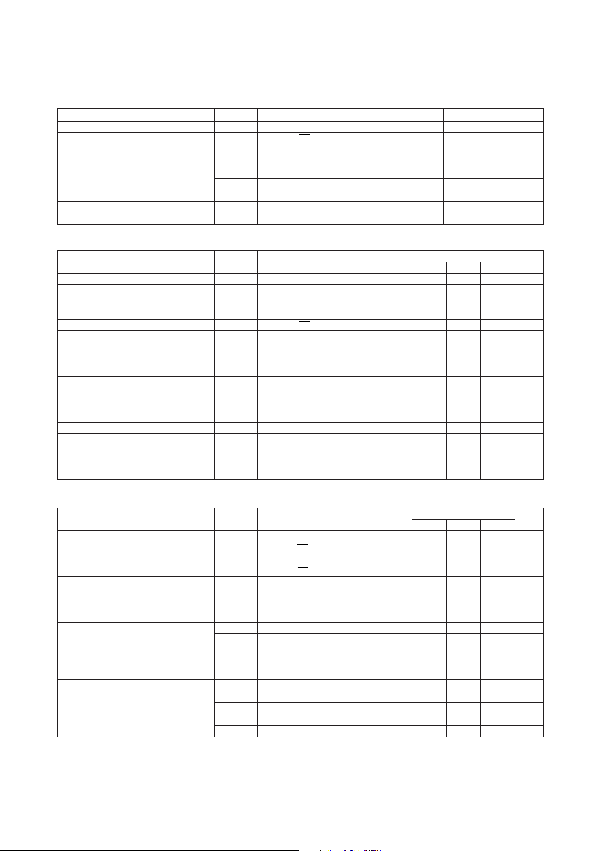
Note: *Except the bias voltage generation divider resistors that are built into VDD1 and VDD2. (See figure 1.)
tinU
V
V
V
V
V
No.4467–2/11
Page 3
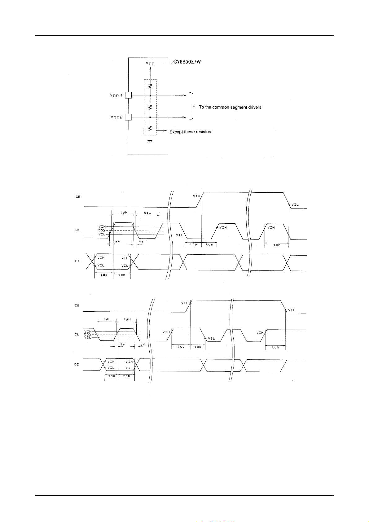
When CL is stopped at the low level
LC75850E, 75850W
Figure 1
When CL is stopped at the high level
Figure 2
No.4467–3/11
Page 4
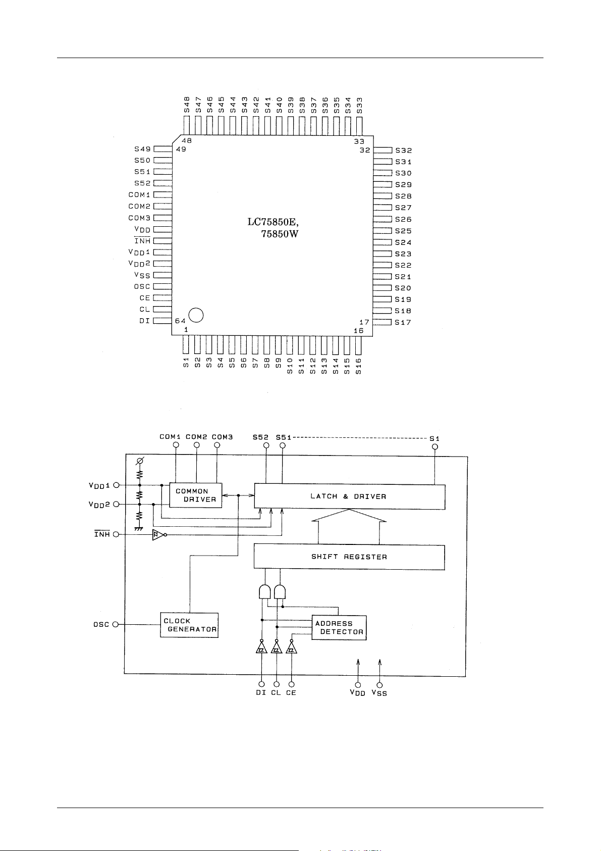
Pin Assignment
LC75850E, 75850W
Block Diagram
Top view
No.4467–4/11
Page 5

LC75850E, 75850W
Pin Functions
niP.oNniPnoitcnuFevitcAO/I
25Sot1S25ot1 atadlairessaderrefsnartatadehtyalpsidtahtstuptuotnemgeS –OnepO
1MOC
2MOC
3MOC
CSO16
EC
LC
ID
HNI75
VDD185
VDD295
Serial Data Transfer Format
1. Serial data
35
45
55
noitcennocrotallicsO
26
36
46
.rossecorporcim
VottcennoC
DD
VottcennoC
DD
fsiycneuqerfemarfehT.stuptuorevirdnommoC
f(=
O
ehtotdetcennoc:sniprefsnartatadlaireS
.desusisaib2/1nehw2
.desusisaib2/1nehw1
.zH)483/–OnepO
CSO
)mrofevawnoitanretlatnemgesnommocehtgnitarenegrof(
elbanepihc:ECH
atadrefsnart:ID–
.atadlanretniehtrofdragertuohtiwyalpsidehtffosnrutylbicroF
.nipsihtfoetatsehtrevetahw,tupniebsyawlanacatadlaireS
.yllanretxededivorperasegatlovsaibnehwegatlovsaib3/2ehtrofdesU
.yllanretxededivorperasegatlovsaibnehwegatlovsaib3/1ehtrofdesU
–IDNG
IDNGkcolcnoitazinorhcnys:LCL→ H
LIDNG
–InepO
–InepO
gnildnaH
desununehw
2. Data transfer format
3. When used with fewer than 156 segments
<Example> Using 63 segments
Segment allocation method……Sixty three segments are allocated starting at D156.
No.4467–5/11
Page 6

LC75850E, 75850W
• CCB address ..........41
• D1 to D156 ............Display data
• DR..........................Drive method selection bit
1 = 1/3 duty, 1/3 bias
0 = 1/3 duty, 1/2 bias
• SC .......................... Segment drive/clear control bit
1 = Clear (Display clearing waveforms are output from common and segment pins.)
0 = Drive (Normal drive)
• BU..........................Normal mode/power saving mode control bit
1 = Power saving mode (The oscillator is stopped and the common and segment pins go to
the ground level.)
0 = Normal mode
• * ............................. Dont’t care
Transferred Data/Output Pin Correspondence
3MOC2MOC1MOC
1S1D2D3D
2S4D5D6D
3S7D8D9D
4S01D11D21D
5S31D41D51D
6S61D71D81D
7S91D02D12D
8S22D32D42D
9S52D62D72D
01S82D92D03D
11S13D23D33D
21S43D53D63D
31S73D83D93D
41S04D14D24D
51S34D44D54D
61S64D74D84D
71S94D05D15D
81S25D35D45D
91S55D65D75D
02S85D95D06D
12S16D26D36D
22S46D56D66D
32S76D86D96D
42S07D17D27D
52S37D47D57D
62S67D77D87D
3MOC2MOC1MOC
72S97D08D18D
82S28D38D48D
92S58D68D78D
03S88D98D09D
13S19D29D39D
23S49D59D69D
33S79D89D99D
43S001D101D201D
53S301D401D501D
63S601D701D801D
73S901D011D111D
83S211D311D411D
93S511D611D711D
04S811D911D021D
14S121D221D321D
24S421D521D621D
34S721D821D921D
44S031D131D231D
54S331D431D531D
64S631D731D831D
74S931D041D141D
84S241D341D441D
94S541D641D741D
05S841D941D051D
15S151D251D351D
25S451D551D651D
No.4467–6/11
Page 7

1/2 Bias, 1/3 Duty Drive Technique
COM1
COM2
COM3
LCD driver output when all LCD
segments corresponding to COM1,
COM2, and COM3 are turned off.
LCD driver output when only LCD
segments corresponding to COM1
are on.
LCD driver output when only LCD
segments corresponding to COM2
are on.
LC75850E, 75850W
LCD driver output when LCD
segments corresponding to
COM1 and COM2 are on.
LCD driver output when only LCD
segments corresponding to COM3
are on.
LCD driver output when LCD
segments corresponding to
COM1 and COM3 are on.
LCD driver output when LCD
segments corresponding to
COM2 and COM3 are on.
LCD driver output when all LCD
segments corresponding to COM1,
COM2, and COM3 are on.
1/2 Bias, 1/3 Duty Waveforms
No.4467–7/11
Page 8

1/3 Bias, 1/3 Duty Drive Technique
COM1
COM2
COM3
LCD driver output when all LCD
segments corresponding to COM1,
COM2, and COM3 are turned off.
LCD driver output when only LCD
segments corresponding to COM1
are on.
LC75850E, 75850W
LCD driver output when only LCD
segments corresponding to COM2
are on.
LCD driver output when LCD
segments corresponding to
COM1 and COM2 are on.
LCD driver output when only LCD
segments corresponding to COM3
are on.
LCD driver output when LCD
segments corresponding to
COM1 and COM3 are on.
LCD driver output when LCD
segments corresponding to
COM2 and COM3 are on.
LCD driver output when all LCD
segments corresponding to COM1,
COM2, and COM3 are on.
1/3 Bias, 1/3 Duty Waveforms
No.4467–8/11
Page 9

LC75850E, 75850W
INH and Display Control
Since the IC internal data (D1 to D156, DR, SC, and BU) is undefined when power is first applied, INH should be set
low at the same time as power is applied, and data should be transferred from the microprocessor while INH is held
low. When the data transfer has completed, set INH high. This will prevent meaningless displays at power on.
Figure 3
No.4467–9/11
Page 10

Application Circuit Example 1
1/3 Bias (for use with small panels)
LC75850E, 75850W
Application Circuit Example 2
1/3 Bias (for use with normal size panels)
No.4467–10/11
Page 11

Application Circuit Example 3
1/3 Bias (for use with large panels)
LC75850E, 75850W
Specifications of any and all SANYO products described or contained herein stipulate the performance,
characteristics, and functions of the described products in the independent state, and are not guarantees
of the performance, characteristics, and functions of the described products as mounted in the customer's
products or equipment. To verify symptoms and states that cannot be evaluated in an independent device,
the customer should always evaluate and test devices mounted in the customer's products or equipment.
SANYO Electric Co., Ltd. strives to supply high-quality high-reliability products. However, any and all
semiconductor products fail with some probability. It is possible that these probabilistic failures could
give rise to accidents or events that could endanger human lives, that could give rise to smoke or fire,
or that could cause damage to other property. When designing equipment, adopt safety measures so
that these kinds of accidents or events cannot occur. Such measures include but are not limited to protective
circuits and error prevention circuits for safe design, redundant design, and structural design.
In the event that any or all SANYO products(including technical data,services) described or
contained herein are controlled under any of applicable local export control laws and regulations,
such products must not be exported without obtaining the export license from the authorities
concerned in accordance with the above law.
No part of this publication may be reproduced or transmitted in any form or by any means, electronic or
mechanical, including photocopying and recording, or any information storage or retrieval system,
or otherwise, without the prior written permission of SANYO Electric Co. , Ltd.
Any and all information described or contained herein are subject to change without notice due to
product/technology improvement, etc. When designing equipment, refer to the "Delivery Specification"
for the SANYO product that you intend to use.
Information (including circuit diagrams and circuit parameters) herein is for example only ; it is not
guaranteed for volume production. SANYO believes information herein is accurate and reliable, but
no guarantees are made or implied regarding its use or any infringements of intellectual property rights
or other rights of third parties.
This catalog provides information as of June, 2001. Specifications and information herein are subject to
change without notice.
PS No.4467–11/11
 Loading...