

Page 1

Any and all SANYO products described or contained herein do not have specifications that can handle
applications that require extremely high levels of reliability, such as life-support systems, aircraft’s
control systems, or other applications whose failure can be reasonably expected to result in serious
physical and/or material damage. Consult with your SANYO representative nearest you before using
any SANYO products described or contained herein in such applications.
SANYO assumes no responsibility for equipment failures that result from using products at values that
exceed, even momentarily, rated values (such as maximum ratings, operating condition ranges, or other
parameters) listed in products specifications of any and all SANYO products described or contained
herein.
Overview
The LC75842E and LC75842M are 1/2 duty generalpurpose LCD display drivers for applications such as
microprocessor-controlled electronic tuning. They can
drive up to 54 segments directly.
Features
• 1/2 duty, 1/2 bias drive of up to 54 segments
• Serial data input supports CCB* format communication
with the system controller.
• Backup function which is based on a power saving
mode and all segments off functions that are controlled
by serial data.
• High generality, since display data is displayed directly
without decoder intervention.
• The display can be forced to the off state with the INH
pin.
• RC oscillator circuit
*
Package Dimensions
unit: mm
3162C-QFP36
unit: mm
3204-MFP36S
0.1
1.7max
0.3
0.65
(0.9)
(1.5)
19
10
18
19
27
28
36
9.0
0.5
7.0
9.0
7.0
0.15
CMOS IC
92501TN (OT)/41096HA (OT)/61595HA (OT) No. 4966-1/10
SANYO: QFP36
[LC75842E]
SANYO Electric Co.,Ltd. Semiconductor Company
TOKYO OFFICE Tokyo Bldg., 1-10, 1 Chome, Ueno, Taito-ku, TOKYO, 110-8534 JAPAN
General-Purpose 1/2 Duty LCD Display Driver
LC75842E, LC75842M
Ordering number : ENN4966C
• CCB is a trademark of SANYO ELECTRIC CO., LTD.
• CCB is SANYO’s original bus format and all the bus
addresses are controlled by SANYO.
SANYO: MFP36S
[LC75842M]
Page 2
No. 4966-2/10
LC75842E, LC75842M
Specifications
Absolute Maximum Ratings at Ta = 25°C, VSS= 0 V
Parameter Symbol Conditions Ratings Unit
Maximum supply voltage V
DD
max V
DD
–0.3 to +6.5 V
Input voltage
V
IN
1 CE, CL, DI, INH –0.3 to +6.5 V
V
IN
2 OSC –0.3 to VDD+ 0.3 V
Output voltage V
OUT
OSC, S1 to S27, COM1, COM2 –0.3 to VDD+ 0.3 V
Output current
I
OUT
1 S1 to S27 100 µA
I
OUT
2 COM1, COM2 1 mA
Allowable power dissipation Pd max Ta = 85°C 100 mW
Operating temperature Topr –40 to +85 °C
Storage temperature Tstg –55 to +125 °C
Parameter Symbol Conditions
Ratings
Unit
min typ max
Supply voltage V
DDVDD
4.0 5.0 6.0 V
Input high level voltage V
IH
CE, CL, DI, INH 0.8 V
DD
6.0 V
Input low level voltage V
IL
CE, CL, DI, INH 0 0.2 V
DD
V
Recommended external resistance R
OSC
OSC 68 kΩ
Recommended external capacitance C
OSC
OSC 680 pF
Guaranteed oscillator range f
OSC
OSC 25 50 100 kHz
Low level clock pulse width t
øL
CL: Figure 1 160 ns
High level clock pulse width t
øH
CL: Figure 1 160 ns
Data setup time t
ds
CL, DI: Figure 1 160 ns
Data hold time t
dh
CL, DI: Figure 1 160 ns
CE wait time t
cp
CE, CL: Figure 1 160 ns
CE setup time t
cs
CE, CL: Figure 1 160 ns
CE hold time t
ch
CE, CL: Figure 1 160 ns
INH switching time t
c
INH, CE: Figure 3 10 µs
Allowable Operating Ranges at Ta = –40 to +85°C, VSS= 0 V
Parameter Symbol Conditions
Ratings
Unit
min typ max
Hysteresis voltage V
H
CE, CL, DI, INH: VDD= 5.0 V 0.4 V
Input high level current I
IH
CE, CL, DI, INH: VI= 6.0 V 5.0 µA
Input low level current I
IL
CE, CL, DI, INH: VI= 0 V –5.0 µA
Output high level voltage
V
OH
1 S1 to S27: IO= –10 µA VDD– 1.0 V
V
OH
2 COM1, COM2: IO= –100 µA VDD– 0.6 V
Output low level voltage
V
OL
1 S1 to S27: IO= 10 µA 1.0 V
V
OL
2 COM1, COM2: IO= 100 µA 0.6 V
Output middle level voltage
V
MID
1 COM1, COM2: VDD= 6.0 V, IO= ±100 µA 2.4 3.0 3.6 V
V
MID
2 COM1, COM2: VDD= 4.0 V, IO= ±100 µA 1.4 2.0 2.6 V
Oscillator frequency f
OSC
OSC: R
OSC
= 68 kΩ, C
OSC
= 680 pF 40 50 60 kHz
Current drain
I
DD
1 Power saving mode 5 µA
I
DD
2 VDD= 6.0 V, output open, f
OSC
= 50 kHz 1.2 2.0 mA
Electrical Characteristics in the Allowable Operating Ranges
Page 3
No. 4966-3/10
LC75842E, LC75842M
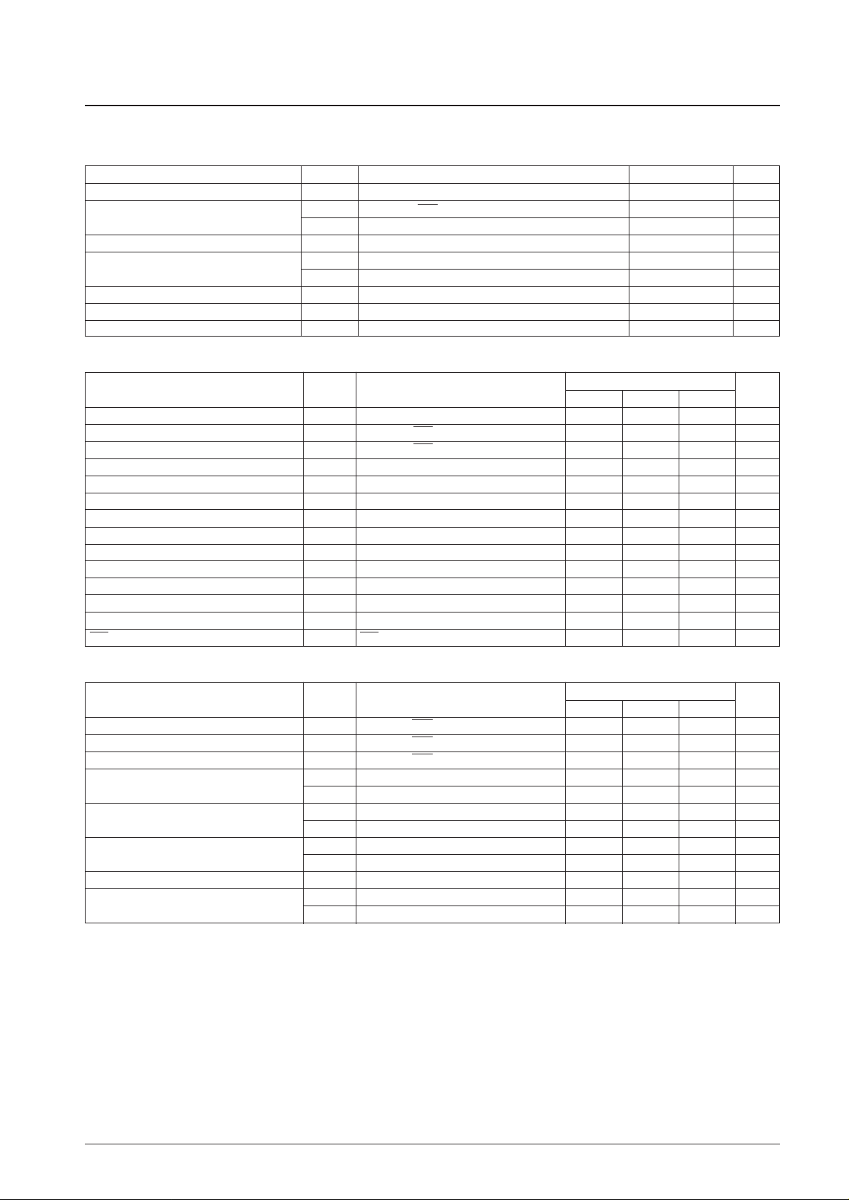
1. When CL is stopped at the low level
tds
DI
CL
CE
V
IH
50%
V
IL
V
IH
V
IL
tdh
tcp tcs tch
tøH tøL
V
IH
V
IL
2. When CL is stopped at the high level
Figure 1
tds tdh
DI
CL
CE
V
IH
50%
V
IL
V
IH
V
IL
tcp tcs tch
tøL tøH
V
IH
V
IL
Pin Assignments
LC75842E
S18
S17
S16
S15
S14
S13
S12
S11
S10
S27
S26
S25
S24
S23
S22
S21
S20
S19
S1S2S3S4S5S6S7S8S9
27 19
28 18
36 10
91
OSC
V
DD
INH
V
SS
CE
CL
DI
COM2
COM1
CE
VSSINH
VDDOSC
S27
S26
S25
S24
S23
S22
S21
S20
S19
S18
S17
S16
S15
CL
DI
COM2
COM1
S1S2S3S4S5S6S7S8S9
S10
S11
S12
S13
S14
36 19
18
1
LC75842M
A03902
A03195
Top view
Top view
Page 4

No. 4966-4/10
LC75842E, LC75842M
Block Diagram
OSC
INH
V
DD
V
SS
COM1
COM2
CE
CL
DI
S 1
S25
S26
S27
COMMON
DRIVER
CLOCK
GENERATOR
CCB INTERFACE
SEGMENT DRIVER & LATCH
SHIFT REGISTER
Pin
Pin No.
Function Active I/O
Handling when
LC75842E LC75842M
unused
S1 to S27
COM1
COM2
OSC
CE
CL
DI
INH
V
DD
V
SS
5 to 31
4
3
32
36
1
2
34
33
35
Segment outputs for displaying the display data transferred by serial data input.
Common driver outputs. The frame frequency f
O
is f
OSC
/512 Hz.
Oscillator connection. An oscillator circuit is formed by connecting an external
resistor and capacitor at this pin.
Serial data transfer inputs. Must be connected to the control microprocessor.
CE: Chip enable
CL: Synchronization clock
DI: Transfer data
Display off control input
INH = low (V
SS
).....Display off (S1 to S27, COM1 and COM2 = low)
INH = high (V
DD
)....Display on
However, serial data transfer is possible when the display is forced off by this
pin.
Power supply. Provide a power supply voltage of between 4.0 and 6.0 V.
Power supply. Connect this pin to ground.
—
—
—
L
—
—
H
—
O
O
I/O
I
I
—
—
Open
Open
V
DD
GND
GND
—
—
Pin Functions
1 to 27
36
35
28
32
33
34
30
29
31
A03196
Page 5
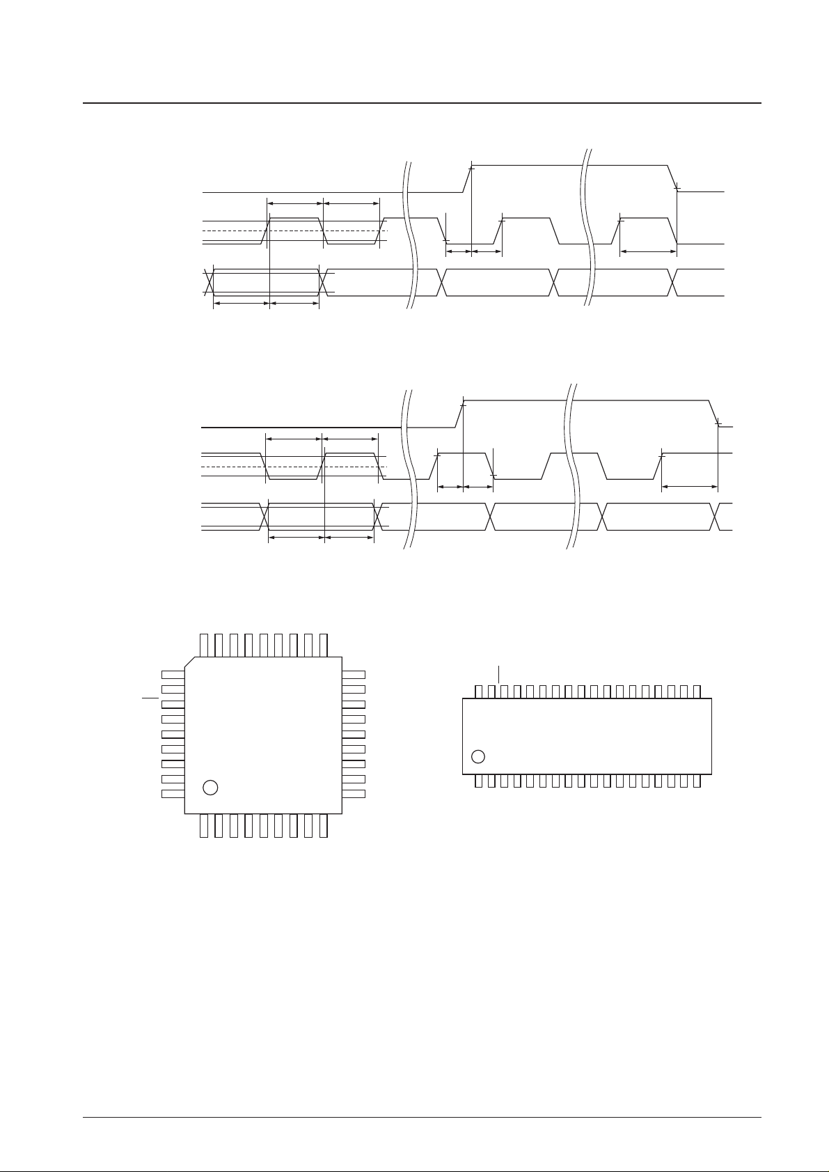
Serial Data Transfer Format
1. When CL is stopped at the low level
No. 4966-5/10
LC75842E, LC75842M
CE
CL
DI
CE
CL
DI
0
B0 B1 B2 B3 A0 A1 A2 A3
B0 B1 B2 B3 A0 A1 A2 A3
0 1 0 0 0 0 D1 D2 D3 D25
D29 D30 D31 D53 D54
D26 D27 D28 BU SC 0 01
0 0 1 0 0 0 0 0 0 0 0 0 11
Control data
4 bits
Display data
28 bits
CCB address
8 bits
CCB address
8 bits
Display data
26 bits
Fixed data
6 bits
A03197
Page 6

2. When CL is stopped at the high level
Figure 2
• CCB address......44
H
• D1 to D54..........Display data
Dn (n = 1 to 54) = 1: Segment on
Dn (n = 1 to 54) = 0: Segment off
• BU.....................Control data for specifying normal mode or power saving mode
• SC......................Control data for specifying all segments on or off
Serial Data Transfer Example
When 29 or more segments are used all 80 bits of the serial data must be sent.
When fewer than 29 segments are used only the first 40 bits of the serial data can be sent. However, all 80 bits must be
sent after power is first applied.
Note: The following type of transfer cannot be used when fewer than 29 segments are used.
No. 4966-6/10
LC75842E, LC75842M
CE
CL
DI
CE
CL
DI
0
B0 B1 B2 B3 A0 A1 A2 A3
B0 B1 B2 B3 A0 A1 A2 A3
0 1 0 0 0 0 D1 D2 D3 D25
D29 D30 D31 D53 D54
D26 D27 D28 BU SC 0 01
0 0 1 0 0 0 0 0 0 0 0 0 11
Control data
4 bits
Display data
28 bits
CCB address
8 bits
CCB address
8 bits
Display data
26 bits
Fixed data
6 bits
B0
0 0 1 00 0 01
B1 B2 B3 A0 A1 A2 A3
D25 D26 D27 BUD28 SC 00D1 D2 D3
B0
0 0 1 00 0 01
B1 B2 B3 A0 A1 A2 A3
D53 D54 0 00 0 10D29 D30 D31
B0
0 0 1 00 0 01
B1 B2 B3 A0 A1 A2 A3
D25 D26 D27 BUD28 SC 00D1 D2 D3
B0
0 0 1 00 0 01
B1 B2 B3 A0 A1 A2 A3
D53 D54 0 00 0 10D29 D30 D31
Page 7

Control Data Functions
1. BU: Control data for specifying normal mode or power saving mode
This control data bit is used to control the normal mode/power saving mode state of the LC75842E and LC75842M.
2. SC: Control data for specifying all segments on or off
This control data bit is used to turn all segments on or off.
Note that when SC is 1 the display is turned off by outputting the segment off waveforms from the segment pins.
Correspondence between Display Data and Segment Output Pins
For example, the table below lists the output states for the S11 segment output pin.
No. 4966-7/10
LC75842E, LC75842M
SC Display state
0 On
1 Off
BU Mode
0 Normal mode
1 Power saving mode (The OSC pin oscillator is stopped and the common and segment output pins go to the V
SS
level.)
Display data
Segment output pin (S11) state
D21 D22
0 0 Both segments for COM1 and COM2 are off.
0 1 Segment for COM2 is on.
1 0 Segment for COM1 is on.
1 1 Both segments for COM1 and COM2 are on.
Segment
COM1 COM2
output pin
S1 D1 D2
S2 D3 D4
S3 D5 D6
S4 D7 D8
S5 D9 D10
S6 D11 D12
S7 D13 D14
S8 D15 D16
S9 D17 D18
S10 D19 D20
S11 D21 D22
S12 D23 D24
S13 D25 D26
S14 D27 D28
Segment
COM1 COM2
output pin
S15 D29 D30
S16 D31 D32
S17 D33 D34
S18 D35 D36
S19 D37 D38
S20 D39 D40
S21 D41 D42
S22 D43 D44
S23 D45 D46
S24 D47 D48
S25 D49 D50
S26 D51 D52
S27 D53 D54
Page 8
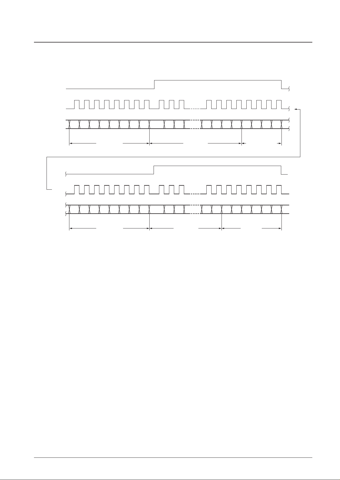
Output Waveforms (1/2 duty, 1/2 bias drive)
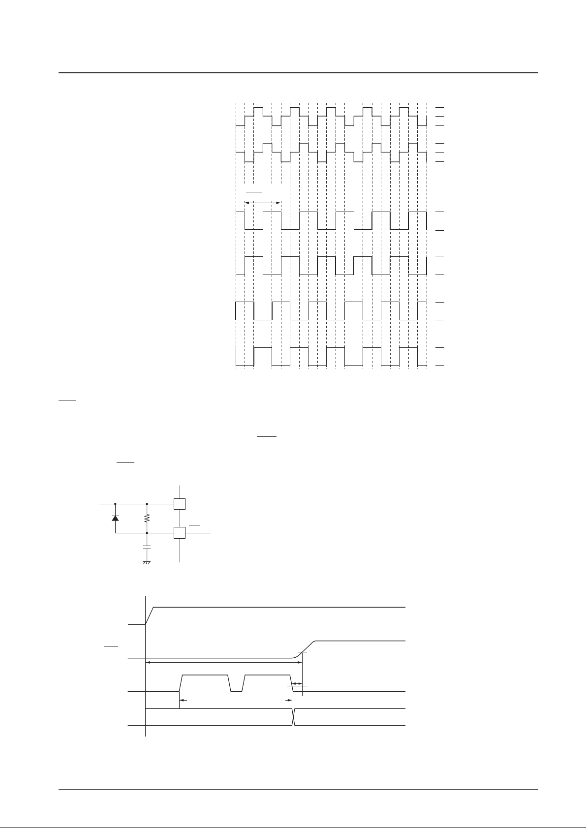
INH and Display Control
Since the IC internal data (D1 to D54 and control data) is undefined when power is first applied, the display is turned off
(S1 to S27, COM1 and COM2 = low) by setting INH pin low at the same time as power is applied. Then, meaningless
display at the power on can be prevented by transferring all 80 bits of serial data from the controller while the display is
turned off and INH pin high after the transfer completes. (See Figure 3.)
Figure 3
No. 4966-8/10
LC75842E, LC75842M
COM1
COM2
V
DD
1/2V
DD
V
SS
f
OSC
512
[Hz]
S1 to S27 output when LCD
segments corresponding to
COM1 are on
S1 to S27 output when LCD
segments corresponding to
both COM1 and COM2 are on
S1 to S27 output when LCD
segments corresponding to
both COM1 and COM2 are
turned off
S1 to S27 output when LCD
segments corresponding to
COM2 are on
V
DD
1/2V
DD
V
SS
V
DD
V
SS
V
DD
V
SS
V
DD
V
SS
V
DD
V
SS
INH
V
DD
R
C
Internal data
CE
INH
V
DD
Defined
t1tc: Determined by the RC circuit
: 10 µs min.
Undefined
t1
tc
VIL
VIL
Display data and control data
transfer
A03198
A03199
A03200
Page 9

Notes on Transferring Display Data from the Controller
Since the LC75842E and LC75842M take the display data (D1 to D54) in two separate transfer operations as shown in
Figure 2, we recommend that all the display data be transferred within 30 [ms] to maintain the quality of the displayed
image.
Sample Display
Sample Application Circuit 1
Sample Application Circuit 2
No. 4966-9/10
LC75842E, LC75842M
Example in which 40 segments are used (up to 54 segments can be used)
③ ① ⑦ ⑦ ⑦ ③ ①
MHz
kHz
FM
MW
LW
STEREO①MONO①AUTO TUNE
①
CH
⑧
Note: The numbers in circles indicate the number of segments.
680 pF
OSC
INH
CE
CL
DI
V
DD
V
SS
COM1
S1
S26
S27
COM2
S2
68 kΩ
From the controller
+5V
+
LCD panel (up to 54 segments)
680 pF
OSC
INH
CE
CL
DI
V
DD
V
SS
COM1
S1
S26
S27
COM2
S2
68 kΩ
+5V
+
From the controller
LCD panel (up to 54 segments)
A03201
A03202
Page 10
PS No. 4966-10/10
LC75842E, LC75842M
This catalog provides information as of September, 2001. Specifications and information herein are
subject to change without notice.
Specifications of any and all SANYO products described or contained herein stipulate the performance,
characteristics, and functions of the described products in the independent state, and are not guarantees
of the performance, characteristics, and functions of the described products as mounted in the customer’s
products or equipment. To verify symptoms and states that cannot be evaluated in an independent device,
the customer should always evaluate and test devices mounted in the customer’s products or equipment.
SANYO Electric Co., Ltd. strives to supply high-quality high-reliability products. However, any and all
semiconductor products fail with some probability. It is possible that these probabilistic failures could
give rise to accidents or events that could endanger human lives, that could give rise to smoke or fire,
or that could cause damage to other property. When designing equipment, adopt safety measures so
that these kinds of accidents or events cannot occur. Such measures include but are not limited to protective
circuits and error prevention circuits for safe design, redundant design, and structural design.
In the event that any or all SANYO products (including technical data, services) described or contained
herein are controlled under any of applicable local export control laws and regulations, such products must
not be exported without obtaining the export license from the authorities concerned in accordance with the
above law.
No part of this publication may be reproduced or transmitted in any form or by any means, electronic or
mechanical, including photocopying and recording, or any information storage or retrieval system,
or otherwise, without the prior written permission of SANYO Electric Co., Ltd.
Any and all information described or contained herein are subject to change without notice due to
product/technology improvement, etc. When designing equipment, refer to the “Delivery Specification”
for the SANYO product that you intend to use.
Information (including circuit diagrams and circuit parameters) herein is for example only; it is not
guaranteed for volume production. SANYO believes information herein is accurate and reliable, but
no guarantees are made or implied regarding its use or any infringements of intellectual property rights
or other rights of third parties.
 Loading...