

Page 1
Any and all SANYO products described or contained herein do not have specifications that can handle
applications that require extremely high levels of reliability, such as life-support systems, aircraft’s
control systems, or other applications whose failure can be reasonably expected to result in serious
physical and/or material damage. Consult with your SANYO representative nearest you before using
any SANYO products described or contained herein in such applications.
SANYO assumes no responsibility for equipment failures that result from using products at values that
exceed, even momentarily, rated values (such as maximum ratings, operating condition ranges,or other
parameters) listed in products specifications of any and all SANYO products described or contained
herein.
CMOS IC
LCD Driver with Level Meter
Ordering number:ENN2292B
LC7583N
SANYO Electric Co.,Ltd. Semiconductor Company
TOKYO OFFICE Tokyo Bldg., 1-10, 1 Chome, Ueno, Taito-ku, TOKYO, 110-8534 JAPAN
Overview
The LC7583N is an LCD driver that can be microcomputercontrolled to provide segment display and level meter dis-
play.
Features
• The serial data address is “5”.
• 1/2duty, 1/2bias, 66 segments (max) (Except ADC output, DSP input display).
• 5-bit AD converter and three selections of level output
shown below.
(1) 13 dots x 2ch Log scale
(2) 13 dots x 2ch Linear scale
(3) 26 dots x 1ch Linear scale
• 2 display (DSP) pins for direct display.
• Microcomputer-controlled data input using 3 pins for serial data input and control.
• The full scale of the AD converter is 31/48Vref. The Vref
is variable (with Vref pin).
• Available for increased use in general-purpose applications because no decoder is required to display the segment data.
• Control bits used to cause the segment output and AD
output to be lighted/unlighted.
• RES pin used to cause the initial mode to be entered.
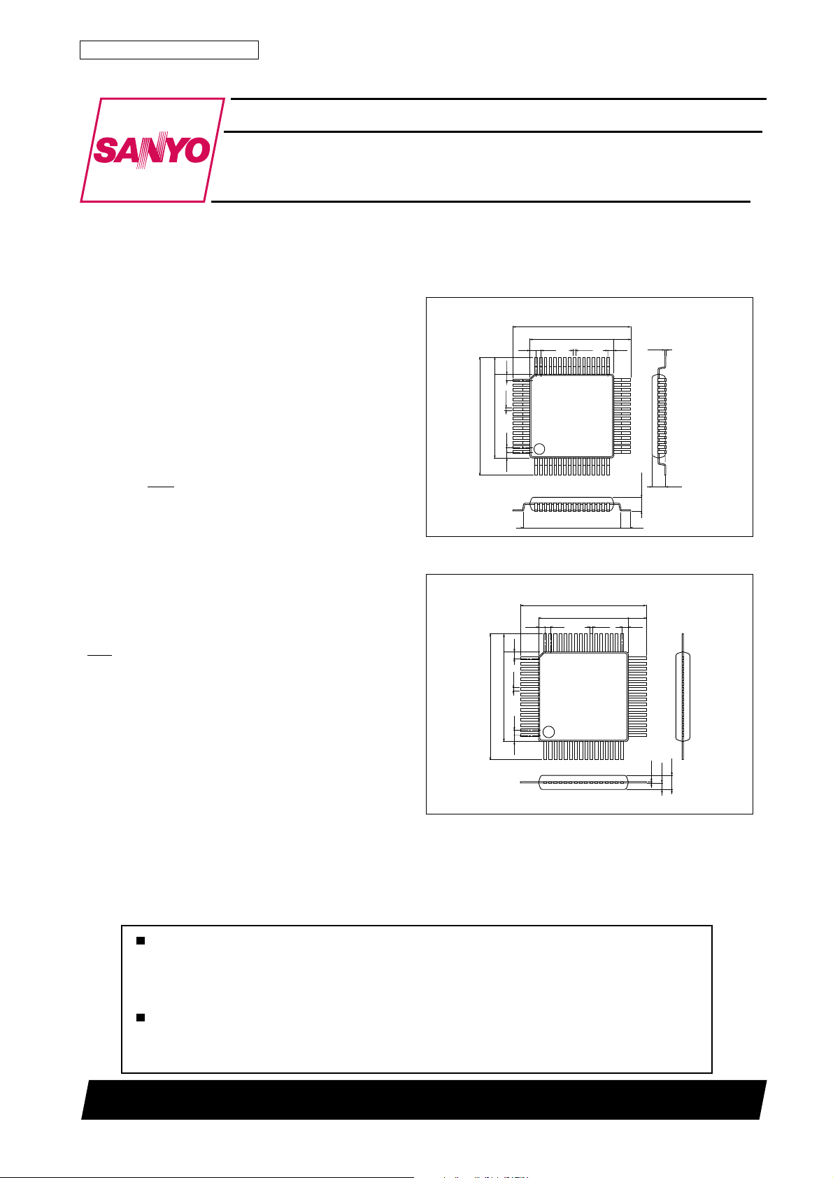
Package Dimensions
unit:mm
3057-QIP64A
[LC7583N]
20.0
14.0
0.8
0.8
1
0.35
16.6
[LC7583N]
19.6
14.0
3.0
1.0
0.35
20.0
14.0
0.8
1.0
unit:mm
3026B-QIP64B
2.8
19.6
14.0
1.0
48
49
64
116
1.0
48
1.0
49
0.35
0.8
64
1.0
0.35
3.0
0.15
1.0
33
32
17
2.45max
1.7
2.8
1.0
33
32
17
16
0.15
2.15
SANYO : QIP64A
2.15
1.0
62001TN (KT)/N111JN/3168KI/N266AT, TS No.2292–1/9
SANYO : QIP64B
Page 2
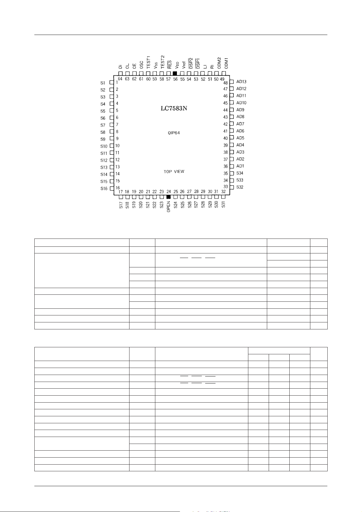
Pin Assignment
LC7583N
Specifications
Absolute Maximum Ratings at Ta = 25˚C, VSS=0V
retemaraPlobmySsnoitidnoCsgnitaRtinU
egatlovylppusmumixaMV
egatlovtupnI
egatlovtuptuOV
tnerructuptuO
noitapissidrewopelbawollAxamdP 001Wm
erutarepmetgnitarepOrpoT 58+ot04–
erutarepmetegarotSgtsT 521+ot54–
Allowable Operating Conditions at Ta = –40 to +85˚C, VSS=0V
retemaraPlobmySsnoitidnoC
egatlovylppuSV
egatlovecnerefeRferVferV ≤V
egatlovlevel-hgihtupnIV
egatlovlevel-woltupnIV
htdiwsiseretsyhtupnIV
ecnatsiserlanretxedednemmoceRRCSO74kΩ
ecnaticapaclanretxedednemmoceRCCSO0001Fp
egnardeetnaraugCSOf
htdiweslupkcolclevel-woLt
htdiweslupkcolclevel-hgiHt
emitputeSt
htdiweslupatadlaireS
emitdlohataDt
emitnoisrevnocDAt
egatlovtupnIV
xamV
DD
VNI12PSD,1PSD,SER.ID,LC,EC
VNI2IL,IRVot3.0–
VNI3ferVVot3.0–
VNI4FFOtuptuoCSOVot3.0–
I
TUO
I
TUO
DD
H
φL
φH
pus
t
1
t
2
hd
NI
DD
TUO
131DAot1DA,43Sot1S 005Aµ
22,1MOC 1Am
Ta≤85°C
1HI
1LI
CSO012305zHk
CSO
VNOC
ID,LC5.0sµ
ID,LC5.0sµ
ID,LC5.0sµ
ID,LC5.0sµ
FFOtuptuoCSOVot3.0–
DD
ID,LC,EC
.A.gifeesEC,LC2sµ
.A.gifeeS 3sµ
lennahcrep,IL,IR002sµ
V/IL,IR
≤ ferV0V
NI
sgnitaR
nimpytxam
5.45.6V
5.4V
2PSD,1PSD,SER,ID,LC,ECV7.0
2PSD,1PSD,SER,ID,LC,EC0V3.0
DD
V50.0
D
V01.0
D
DD
0.7+ot3.0–V
0.7+ot3.0–V
VDD3.0+V
3.0+V
DD
3.0+V
DD
3.0+V
DD
3.0+V
DD
˚C
˚C
tinU
V
DD
5.6V
V
DD
V
V
DD
No.2292–2/9
Page 3
LC7583N
Electrical Characteristics at Ta = 25˚C, under Allowable Operating Conditions
retemaraPlobmySsnoitidnoC
tnerruclevel-hgihtupnII
tnerruclevel-woltupnII
egatlovlevel-hgihtuptuOV
egatlovlevel-woltuptuOV
egatlovlevel-hgihtuptuOV
egatlovlevel-woltuptuOV
egatlovlevel-MV
egatlovlevel-MV
ycneuqerfCSOf
rorreytiraenilnoisrevnocDArrEV5.6ot5.4=ferV ≤V
tnerrucylppuSI
tnerrucylppusecnerefeRferIferV3.01Am
Block Diagram
1HI
1LI
1HO
1LO
2HO
2LO
DIM
DIM
CSO
f
DD
I,43Sot1S
Aµ01–=V
O
I,31DAot1DA
Aµ01=0.1V
O
I,2MOC,1MOC
I,2MOC,1MOC
V,2MOC,1MOC
V,2MOC,1MOC
k74=R,CSO Ω Fp0001=C,23zHk
CSO
Aµ001–=V
O
Aµ001=6.0V
O
I,V5.6=
DD
I,V0.3=
DD
DD
V=tupni,zHk23=
DO
Aµ001±=56.252.358.3V
O
Aµ001±=9.05.11.2V
O
nepo=tuptuo,24Am
sgnitaR
nimpytxam
V5.6=IV,2PSD,1PSD,SER,IL,IR,ID,LC,EC 5Aµ
V0=IV,2PSD,1PSD,SER,IL,IR,ID,LC,EC 5Aµ
0.1–V
DD
6.0–V
DD
2/1–2/1+BSL
tinU
No.2292–3/9
Page 4

LC7583N
Pin Function
emaNniP.oNniPnoitpircseDevitcAO/InoitarugifnoCO/I
33Sot1S43ot1atadehtyalpsidotdesusniptuptuotnemgeS
43S53lanretxeehtyalpsidotdesuniptuptuotnemgeS
31DAot1DA84ot63tupniCDAehtyalpsidotdesusniptuptuotnemgeS
1MOC
2MOC
IR
IL
1PSD
2PSD
ferV55ecnereferretrevnocDAehtylppusotdesuniP
V
DD
V
SS
SER75ehttadethgilnuebotyalpsidehtecrofotdesuniP
2TSET85nepO–O–
1TSET06VotdetcennocronepO
EC26
LC36
ID46
NEPO42.noitcennocoN–––
94
05
15
25
35
45
65
95
.atad)1L,1R(
.nrettap
.egatlov
.edomlaitini
atad)2PSD,1PSD(tupni
,levelgnithgiltsewoL:1DA
levelgnithgiltsehgiH:31DA
.sniptuptuorevirdnommoC
f:ycneuqerfemarF
.nipylppusrewoP
elbanepihC:EC
kcolccnyS:LC
atadrefsnarT:ID
zH215/
CSO
.sniptupniretrevnocDA
.43Stadereviledsituptuo
.–IA
SS
.niprefsnartatadlaireS
.niptupniatadlairesehtmorfderrefsnart
tnemgesesohwsnipyalpsid)tupnilanretxe(tceriD
.)retupmocorcim(rellortnocaotdetcennoC
–O
–O
fosepyt3edivorpotdesuera"2A","1A"stiblortnoC
–O
–O C
golanAI E
LI A
–– –
–– –
LI A
H
ID
–
B
Equivalent Input/Output Configuration
No.2292–4/9
Page 5

ADC Display Mode
2ch (stereo) Display (shown for one channel only)
LC7583N
Lighting Level for Log Display
yalpsiD
tuptuO
1DA0.02–8DA0.0
2DA0.41–9DA0.1
3DA5.01–01DA0.3
4DA0.8–11DA0.5
5DA5.4–21DA0.8
6DA0.3–31DA0.01
7DA0.1–
Note) The conversion error of the AD converter is ±1/2LSB.
When 0dB is taken as 1V (at Vref=4.95V), a conversion error of
approximately ±3.5dB occurs at –20dB.
COMMON Connection
yalpsiDBd
)Bd(
yalpsiD
tuptuO
yalpsiDBd
)Bd(
No.2292–5/9
Page 6

1ch (monaural) Display
LC7583N
Connect the RI pin and LI pin at the monaural mode.
ADC Conversion Time
When the oscillation frequency is 32kHz, individual input signals at the RI pin, LI pin are sampling-processed alternately once every 1ms.
No.2292–6/9
Page 7

Connection of Serial Data, DSP Input Data
RES Pin and Display Control
The internal circuit of the RES pin is shown below.
LC7583N
No.2292–7/9
Page 8

Output Waveforms (S1 to S34, AD1 to AD13)
LC7583N
Sample Application Circuit
[Fig. A] : Data Transfer Mode (Transferred from a controller as shown below)
No.2292–8/9
Page 9

LC7583N
Serial Data
· Address of LC7583 : “1010” is transferred as shown above.
· D1 to D66 : Display data Lighted at “1”
Unlighted at “0”
· X : don’t care
· SC : Control bit used to cause S1 to S34 to be lighted/unlighted.
Unlighted at “1”
Lighted at “0”
· MC : Control bit used to cause AD1 to AD13 to be lighted/unlighted.
Unlighted at “1”
Lighted at “0”
· A1, A2 : Bits used to select the AD converter display mode.
2A1AedoMyalpsiD
00 hc2xstod31elacsgoL
01 hc2xstod31elacsraeniL
10
11
hc1xstod62elacsraeniL
· Sample transfer
· Using ADC only
· Using ADC and segment 10 bits (The segment outputs are delivered at S29 to S33.)
Specifications of any and all SANYO products described or contained herein stipulate the performance,
characteristics, and functions of the described products in the independent state, and are not guarantees
of the performance, characteristics, and functions of the described products as mounted in the customer's
products or equipment. To verify symptoms and states that cannot be evaluated in an independent device,
the customer should always evaluate and test devices mounted in the customer's products or equipment.
SANYO Electric Co., Ltd. strives to supply high-quality high-reliability products. However, any and all
semiconductor products fail with some probability. It is possible that these probabilistic failures could
give rise to accidents or events that could endanger human lives, that could give rise to smoke or fire,
or that could cause damage to other property. When designing equipment, adopt safety measures so
that these kinds of accidents or events cannot occur. Such measures include but are not limited to protective
circuits and error prevention circuits for safe design, redundant design, and structural design.
In the event that any or all SANYO products(including technical data,services) described or
contained herein are controlled under any of applicable local export control laws and regulations,
such products must not be exported without obtaining the export license from the authorities
concerned in accordance with the above law.
No part of this publication may be reproduced or transmitted in any form or by any means, electronic or
mechanical, including photocopying and recording, or any information storage or retrieval system,
or otherwise, without the prior written permission of SANYO Electric Co. , Ltd.
Any and all information described or contained herein are subject to change without notice due to
product/technology improvement, etc. When designing equipment, refer to the "Delivery Specification"
for the SANYO product that you intend to use.
Information (including circuit diagrams and circuit parameters) herein is for example only ; it is not
guaranteed for volume production. SANYO believes information herein is accurate and reliable, but
no guarantees are made or implied regarding its use or any infringements of intellectual property rights
or other rights of third parties.
This catalog provides information as of June, 2001. Specifications and information herein are subject to
change without notice.
PS No.2292–9/9
 Loading...