

Page 1

93098HA (OT)/N3095HA (OT) No.5252-1/17
Overview
The LC75824E and LC75824W are 1/4 duty generalpurpose LCD display drivers that can be used for
frequency display in electronic tuners under the control of
a microcontroller. In addition to being able to directly
drive up to 204 LCD segments, the LC75824E and
LC75824W can also control up to 12 general-purpose
output ports.
Features
• Support for 1/4 duty 1/2 bias or 1/4 duty 1/3 bias drive
of up to 204 segments under serial data control
• Serial data input supports CCB* format communication
with the system controller.
• Serial data control of the power-saving mode based
backup function and all the segments forced off function
• Serial data control of switching between the segment
output port and general-purpose output port functions
• Serial data control of the normal mode current drain
• High generality since display data is displayed directly
without decoder intervention.
• The INH pin can force the display to the off state.
• RC oscillator circuit
Package Dimensions
unit: mm
3159-QFP64E
SANYO: QFP64E
[LC75824E]
unit: mm
3190-SQFP64
SANYO: SQFP64
[LC75824W]
• CCB is a trademark of SANYO ELECTRIC CO., LTD.
• CCB is SANYO’s original bus format and all the bus
addresses are controlled by SANYO.
CMOS LSI
Ordering number : EN5252A
1/4 Duty General-Purpose LCD Display Driver
LC75824E, 75824W
SANYO Electric Co.,Ltd. Semiconductor Bussiness Headquarters
TOKYO OFFICE Tokyo Bldg., 1-10, 1 Chome, Ueno, Taito-ku, TOKYO, 110-8534 JAPAN
Any and all SANYO products described or contained herein do not have specifications that can handle
applications that require extremely high levels of reliability, such as life-support systems, aircraft’s
control systems, or other applications whose failure can be reasonably expected to result in serious
physical and/or material damage. Consult with your SANYO representative nearest you before using
any SANYO products described or contained herein in such applications.
SANYO assumes no responsibility for equipment failures that result from using products at values that
exceed, even momentarily, rated values (such as maximum ratings, operating condition ranges, or other
parameters) listed in products specifications of any and all SANYO products described or contained
herein.
Page 2

Pin Assignment
Specifications
Absolute Maximum Ratings at Ta = 25°C, VSS= 0 V
No.5252-2/17
LC75824E, 75824W
Parameter Symbol Conditions Ratings Unit
Maximum supply voltage V
DD
max V
DD
–0.3 to +7.0 V
Input voltage
V
IN
1 CE, CL, DI, INH –0.3 to +7.0
V
V
IN
2 OSC, VDD1, VDD2 –0.3 to VDD+ 0.3
Output voltage V
OUT
OSC, S1 to S51, COM1 to COM4, P1 to P12 –0.3 to VDD+ 0.3 V
I
OUT
1 S1 to S51 300 µA
Output current I
OUT
2 COM1 to COM4 3
mA
I
OUT
3 P1 to P12 5
Allowable power dissipation Pd max Ta = 85°C 200 mW
Operating temperature Topr –40 to +85 °C
Storage temperature Tstg –55 to +125 °C
Top view
Page 3

Allowable Operating Ranges at Ta = –40 to 85°C, VSS= 0 V
Electrical Characteristics for the Allowable Operating Ranges
Note: * Excluding the bias voltage generation divider resistors built into the VDD1 and VDD2. (See Figure 1)
No.5252-3/17
LC75824E, 75824W
Parameter Symbol Conditions min typ max Unit
Supply voltage V
DD
V
DD
3.0 6.0 V
Input voltage
V
DD
1 VDD1 2/3 V
DD
V
DD
V
V
DD
2 VDD2 1/3 V
DD
V
DD
Input high-level voltage V
IH
CE, CL, DI, INH 0.8 V
DD
6.0 V
Input low-level voltage V
IL
CE, CL, DI, INH 0 0.2 V
DD
V
Recommended external
R
OSC
OSC 270 kΩ
resistance
Recommended external
C
OSC
OSC 100 pF
capacitance
Guaranteed oscillation range f
OSC
OSC 25 50 100 kHz
Data setup time t
ds
CL, DI: Figure 2 160 ns
Data hold time t
dh
CL, DI: Figure 2 160 ns
CE wait time t
cp
CE, CL: Figure 2 160 ns
CE setup time t
cs
CE, CL: Figure 2 160 ns
CE hold time t
ch
CE, CL: Figure 2 160 ns
High-level clock pulse width t
øH
CL: Figure 2 160 ns
Low-level clock pulse width t
øL
CL: Figure 2 160 ns
Rise time t
r
CE, CL, DI: Figure 2 160 ns
Fall time t
f
CE, CL, DI: Figure 2 160 ns
INH switching time t
c
INH, CE: Figure 3 10 µs
Parameter Symbol Conditions min typ max Unit
Hysteresis V
H
CE, CL, DI, INH 0.1 V
DD
V
Input high-level current I
IH
CE, CL, DI, INH: VI= 6.0 V 5.0 µA
Input low-level current I
IL
CE, CL, DI, INH: VI= 0 V –5.0 µA
V
OH
1 S1 to S51: IO= –20 µA VDD– 1.0
Output high-level voltage V
OH
2 COM1 to COM4: IO= –100 µA VDD– 1.0 V
V
OH
3 P1 to P12: IO= –1 mA VDD– 1.0
V
OL
1 S1 to S51: IO= 20 µA 1.0
Output low-level voltage V
OL
2 COM1 to COM4: IO= 100 µA 1.0 V
V
OL
3 P1 to P12: IO= 1 mA 1.0
V
MID
1 COM1 to COM4: 1/2 bias, IO= ±100 µA
1/2 VDD– 1.0 1/2 VDD+ 1.0
V
MID
2 S1 to S51: 1/3 bias, IO= ±20 µA
2/3 VDD– 1.0 2/3 VDD+ 1.0
Output middle-level voltage* V
MID
3 S1 to S51: 1/3 bias, IO= ±20 µA
1/3 VDD– 1.0 1/3 VDD+ 1.0
V
V
MID
4 COM1 to COM4: 1/3 bias, IO= ±100 µA
2/3 VDD– 1.0 2/3 VDD+ 1.0
V
MID
5 COM1 to COM4: 1/3 bias, IO= ±100 µA
1/3 VDD– 1.0 1/3 VDD+ 1.0
Oscillator frequency f
OSC
OSC: R
OSC
= 270 kΩ, C
OSC
= 100 pF 40 50 60 kHz
I
DD
1 Power-saving mode 5
I
DD
2
V
DD
= 3.0 V, outputs open, 1/2 bias, f
OSC
= 50 kHz,
70 140
control data CU = 0
I
DD
3
V
DD
= 6.0 V, outputs open, 1/2 bias, f
OSC
= 50 kHz,
200 400
control data CU = 0
I
DD
4
V
DD
= 3.0 V, outputs open, 1/3 bias, f
OSC
= 50 kHz,
80 160
control data CU = 0
I
DD
5
V
DD
= 6.0 V, outputs open, 1/3 bias, f
OSC
= 50 kHz,
250 500
Current drain
control data CU = 0
µA
I
DD
6
V
DD
= 3.0 V, outputs open, 1/2 bias, f
OSC
= 50 kHz,
30 60
control data CU = 1
I
DD
7
V
DD
= 6.0 V, outputs open, 1/2 bias, f
OSC
= 50 kHz,
130 260
control data CU = 1
I
DD
8
V
DD
= 3.0 V, outputs open, 1/3 bias, f
OSC
= 50 kHz,
40 80
control data CU = 1
I
DD
9
V
DD
= 6.0 V, outputs open, 1/3 bias, f
OSC
= 50 kHz,
150 300
control data CU = 1
Page 4
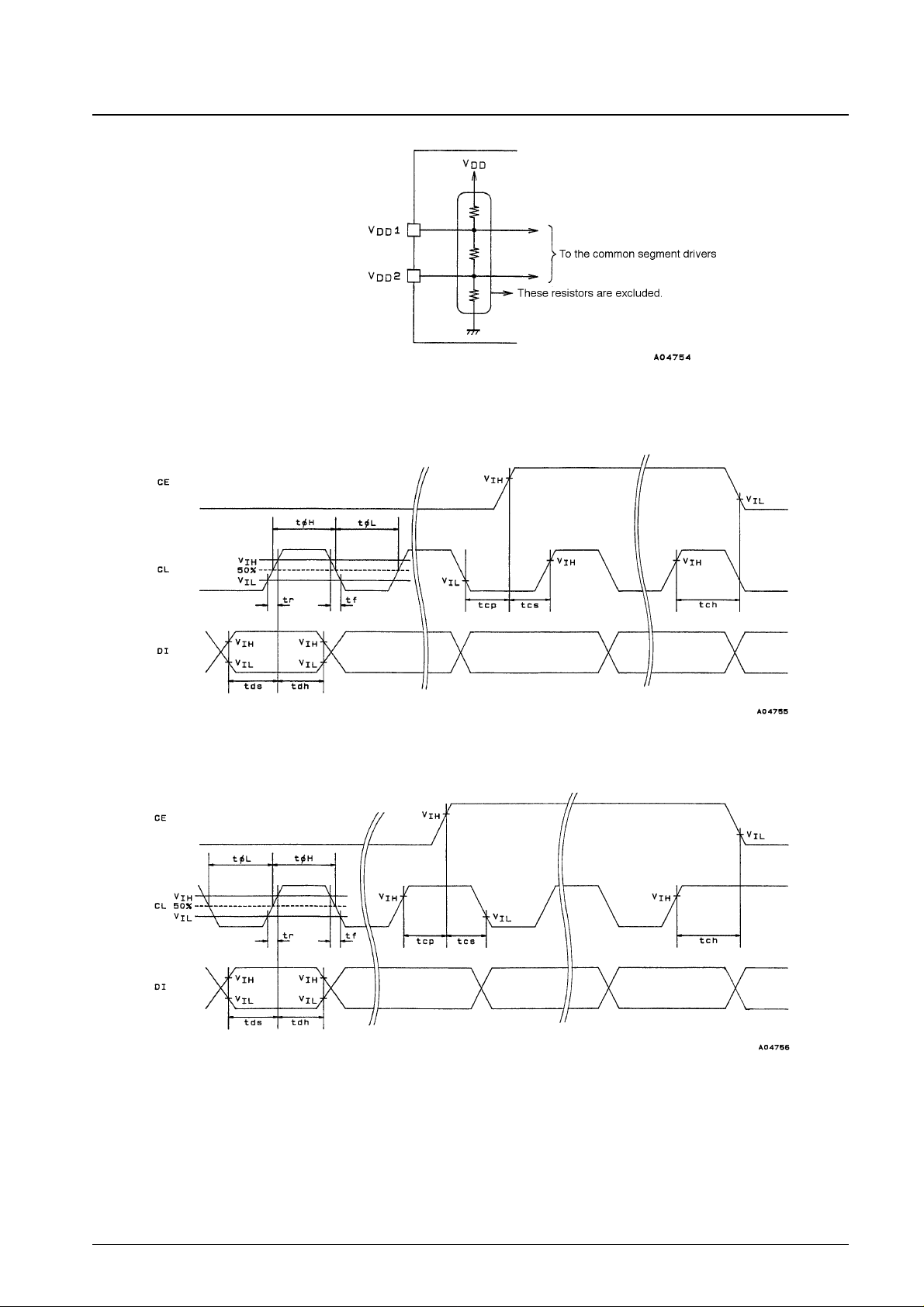
Figure 1
1. When CL is stopped at the low level
2. When CL is stopped at the high level
Figure 2
No.5252-4/17
LC75824E, 75824W
Page 5

Block Diagram
Pin Functions
No.5252-5/17
LC75824E, 75824W
Pin Pin No. Function Active I/O
Handling when
unused
S1/P1 to S12/P12,
S13 to S51
COM1 to COM4
OSC
CE
CL
DI
INH
V
DD
1
V
DD
2
V
DD
V
SS
1 to 12,
13 to 51
52 to 55
60
62
63
64
61
57
58
56
59
Segment outputs for displaying the display data transferred by serial data
input. Pins S1/P1 to S12/P12 can be used as general-purpose output ports
when so specified by the control data.
Common driver outputs.
The frame frequency f
O
is given by: fO = (f
OSC
/512) Hz.
Oscillator connection. An oscillator circuit is formed by connecting an external
resistor and capacitor to this pin.
CE: Chip enable
CL: Synchronization clock
DI: Transfer data
Serial data transfer inputs.
These pins are connected to the
microcontroller.
Display off control input
• INH = low (V
SS
) .......Display forced off
Pins S1/P1 to S12/P12 = low (These pins are forced to
the segment output port
function and held low.)
S13 to S51 = low
COM1 to COM4 = low
• INH = high (V
DD
)......Display on
Note that serial data transfers can be performed when the display is forced off.
Used to apply the LCD drive 2/3 bias voltage. Short this pin to V
DD
2 if a
1/2-bias drive scheme is used.
Used to apply the LCD drive 1/3 bias voltage. Short this pin to V
DD
1 if a
1/2-bias drive scheme is used.
Power supply. Provide a voltage of between 3.0 and 6.0 V.
Ground. Connect this pin to the system ground.
—
—
—
H
—
L
—
—
—
—
O
O
I/O
I
I
I
I
I
I
—
—
Open
Open
GND
GND
GND
Open
Open
—
—
Page 6

Serial Data Input
1. When CL is stopped at the low level
Note: DD is the direction data.
No.5252-6/17
LC75824E, 75824W
CCB address
8 bits
Display data
52 bits
Control data
10 bits
DD
CCB address
8 bits
Display data
52 bits
Fixed data
10 bits
DD
CCB address
8 bits
Display data
52 bits
Fixed data
10 bits
DD
CCB address
8 bits
Display data
48 bits
Fixed data
14 bits
DD
Page 7

2. When CL is stopped at the high level
Note: DD is the direction data.
• CCB address...............41H
• D1 to D204.................Display data
• CU..............................Normal mode current drain control data
• P0 to P3......................Segment output port/general-purpose output port switching control data
• DR..............................1/2-bias drive or 1/3-bias drive switching control data
• SC...............................Segments on/off control data
• BU..............................Normal mode/power-saving mode control data
No.5252-7/17
LC75824E, 75824W
CCB address
8 bits
Display data
52 bits
Control data
10 bits
DD
CCB address
8 bits
Display data
52 bits
Fixed data
10 bits
DD
CCB address
8 bits
Display data
52 bits
Fixed data
10 bits
DD
CCB address
8 bits
Display data
48 bits
Fixed data
14 bits
DD
Page 8

Serial Data Transfer Examples
1. When 157 or more segments are used
All 256 bits of the serial data must be sent.
2. When fewer than 157 segments are used
Either 64 bits, 128 bits, or 192 bits of serial data must be sent, depending on the number of segments actually used.
However, the serial data shown in the figure below (the display data D1 to D52 and the control data) must always be
sent.
No.5252-8/17
LC75824E, 75824W
Page 9

Control Data Functions
1. CU: Normal mode current drain control data
This control data bit controls the current drain in normal mode.
However, note that the common and segment output waveforms are easily caused distortion when the low current
drain mode is selected by setting CU to 1, because in this mode the capacity to supply current to the LCD panel from
the common and segment pins is mode less than that in the normal current drain mode (CU = 0).
2. P0 to P3: Segment output port/general-purpose output port switching control data
These control data bits switch the segment output port/general-purpose output port functions of the S1/P1 to S12/P12
output pins.
Note: Sn (n = 1 to 12): Segment output port function
Pn (n = 1 to 12): General-purpose output port function
When the general-purpose output port function is selected the output pins and the display data have the
correspondence listed in the tables below.
For example, when the general-purpose output port function is selected for the S4/P4 output pin, that output pin will
output a high level when display data D13 is 1, and will output a low level when D13 is 0.
No.5252-9/17
LC75824E, 75824W
CU Current drain mode in normal mode
0 Normal current drain mode (I
DD
2, IDD3, IDD4, and IDD5)
1 Low current drain mode (I
DD
6, IDD7, IDD8, and IDD9)
Output pin Corresponding display data
S1/P1 D1
S2/P2 D5
S3/P3 D9
S4/P4 D13
S5/P5 D17
S6/P6 D21
Output pin Corresponding display data
S7/P7 D25
S8/P8 D29
S9/P9 D33
S10/P10 D37
S11/P11 D41
S12/P12 D45
Control data Output pin states
P0 P1 P2 P3 S1/P1 S2/P2 S3/P3 S4/P4 S5/P5 S6/P6 S7/P7 S8/P8 S9/P9 S10/P10 S11/P11 S12/P12
0 0 0 0 S1 S2 S3 S4 S5 S6 S7 S8 S9 S10 S11 S12
0 0 0 1 P1 S2 S3 S4 S5 S6 S7 S8 S9 S10 S11 S12
0 0 1 0 P1 P2 S3 S4 S5 S6 S7 S8 S9 S10 S11 S12
0 0 1 1 P1 P2 P3 S4 S5 S6 S7 S8 S9 S10 S11 S12
0 1 0 0 P1 P2 P3 P4 S5 S6 S7 S8 S9 S10 S11 S12
0 1 0 1 P1 P2 P3 P4 P5 S6 S7 S8 S9 S10 S11 S12
0 1 1 0 P1 P2 P3 P4 P5 P6 S7 S8 S9 S10 S11 S12
0 1 1 1 P1 P2 P3 P4 P5 P6 P7 S8 S9 S10 S11 S12
1 0 0 0 P1 P2 P3 P4 P5 P6 P7 P8 S9 S10 S11 S12
1 0 0 1 P1 P2 P3 P4 P5 P6 P7 P8 P9 S10 S11 S12
1 0 1 0 P1 P2 P3 P4 P5 P6 P7 P8 P9 P10 S11 S12
1 0 1 1 P1 P2 P3 P4 P5 P6 P7 P8 P9 P10 P11 S12
1 1 0 0 P1 P2 P3 P4 P5 P6 P7 P8 P9 P10 P11 P12
Page 10

3. DR: 1/2 bias drive or 1/3 bias drive switching control data
This control data bit selects either 1/2 bias drive or 1/3 bias drive.
4. SC: Segments on/off control data
This control data bit controls the on/off state of the segments.
However, note that when the segments are turned off by setting SC to 1, the segments are turned off by outputting
segment off waveforms from the segment output pins.
5. BU: Normal mode/power-saving mode control data
This control data bit selects either normal mode or power-saving mode.
No.5252-10/17
LC75824E, 75824W
DR Drive type
0 1/3 bias drive
1 1/2 bias drive
SC Display state
0 On
1 Off
BU Mode
0 Normal mode
1
Power-saving mode. In this mode the OSC pin oscillator is stopped and the common and segment pins output low levels. However,
the S1/P1 to S12/P12 output pins can still be used as general-purpose output ports under the control of the control data bits P0 to P3.
Page 11

Display Data to Output Pin Correspondence
Note: These tables assume that the segment output port function is selected for the S1/P1 to S12/P12 output pins.
The table presents the states of the S21 output pin as an example.
No.5252-11/17
LC75824E, 75824W
Output pin COM1 COM2 COM3 COM4
S1/P1 D1 D2 D3 D4
S2/P2 D5 D6 D7 D8
S3/P3 D9 D10 D11 D12
S4/P4 D13 D14 D15 D16
S5/P5 D17 D18 D19 D20
S6/P6 D21 D22 D23 D24
S7/P7 D25 D26 D27 D28
S8/P8 D29 D30 D31 D32
S9/P9 D33 D34 D35 D36
S10/P10 D37 D38 D39 D40
S11/P11 D41 D42 D43 D44
S12/P12 D45 D46 D47 D48
S13 D49 D50 D51 D52
S14 D53 D54 D55 D56
S15 D57 D58 D59 D60
S16 D61 D62 D63 D64
S17 D65 D66 D67 D68
S18 D69 D70 D71 D72
S19 D73 D74 D75 D76
S20 D77 D78 D79 D80
S21 D81 D82 D83 D84
S22 D85 D86 D87 D88
S23 D89 D90 D91 D92
S24 D93 D94 D95 D96
S25 D97 D98 D99 D100
Output pin COM1 COM2 COM3 COM4
S26 D101 D102 D103 D104
S27 D105 D106 D107 D108
S28 D109 D110 D111 D112
S29 D113 D114 D115 D116
S30 D117 D118 D119 D120
S31 D121 D122 D123 D124
S32 D125 D126 D127 D128
S33 D129 D130 D131 D132
S34 D133 D134 D135 D136
S35 D137 D138 D139 D140
S36 D141 D142 D143 D144
S37 D145 D146 D147 D148
S38 D149 D150 D151 D152
S39 D153 D154 D155 D156
S40 D157 D158 D159 D160
S41 D161 D162 D163 D164
S42 D165 D166 D167 D168
S43 D169 D170 D171 D172
S44 D173 D174 D175 D176
S45 D177 D178 D179 D180
S46 D181 D182 D183 D184
S47 D185 D186 D187 D188
S48 D189 D190 D191 D192
S49 D193 D194 D195 D196
S50 D197 D198 D199 D200
S51 D201 D202 D203 D204
Display data
Output pin (S21) state
D81 D82 D83 D84
0 0 0 0 The LCD segments corresponding to COM1 to COM4 are off.
0 0 0 1 The LCD segment corresponding to COM4 is on (lit).
0 0 1 0 The LCD segment corresponding to COM3 is on.
0 0 1 1 The LCD segments corresponding to COM3 and COM4 are on.
0 1 0 0 The LCD segment corresponding to COM2 is on.
0 1 0 1 The LCD segments corresponding to COM2 and COM4 are on.
0 1 1 0 The LCD segments corresponding to COM2 and COM3 are on.
0 1 1 1 The LCD segments corresponding to COM2, COM3, and COM4 are on.
1 0 0 0 The LCD segment corresponding to COM1 is on.
1 0 0 1 The LCD segments corresponding to COM1 and COM4 are on.
1 0 1 0 The LCD segments corresponding to COM1 and COM3 are on.
1 0 1 1 The LCD segments corresponding to COM1, COM3, and COM4 are on.
1 1 0 0 The LCD segments corresponding to COM1 and COM2 are on.
1 1 0 1 The LCD segments corresponding to COM1, COM2, and COM4 are on.
1 1 1 0 The LCD segments corresponding to COM1, COM2, and COM3 are on.
1 1 1 1 The LCD segments corresponding to COM1 to COM4 are on.
Page 12

1/4 Duty, 1/2 Bias Drive Scheme
1/4 Duty, 1/2 Bias Waveforms
No.5252-12/17
LC75824E, 75824W
LCD driver output for all LCD segments
corresponding to COM1 to COM4 off.
LCD driver output for only the LCD segment
corresponding to COM1 on (lit).
LCD driver output for only the LCD segment
corresponding to COM2 on.
LCD driver output for the LCD segment
corresponding to COM1 and COM2 on.
LCD driver output for only the LCD segment
corresponding to COM3 on.
LCD driver output for the LCD segment
corresponding to COM1 and COM3 on.
LCD driver output for the LCD segment
corresponding to COM2 and COM3 on.
LCD driver output for the LCD segment
corresponding to COM1, COM2, and COM3 on.
LCD driver output for only the LCD segment
corresponding to COM4 on.
LCD driver output for the LCD segment
corresponding to COM2 and COM4 on.
LCD driver output for all LCD segments
corresponding to COM1 to COM4 on.
COM1
COM2
COM3
COM4
Page 13

1/4 Duty, 1/3 Bias Drive Scheme
1/4 Duty, 1/3 Bias Waveforms
No.5252-13/17
LC75824E, 75824W
LCD driver output for all LCD segments
corresponding to COM1 to COM4 off.
LCD driver output for only the LCD segment
corresponding to COM1 on (lit).
LCD driver output for only the LCD segment
corresponding to COM2 on.
LCD driver output for the LCD segment
corresponding to COM1 and COM2 on.
LCD driver output for only the LCD segment
corresponding to COM3 on.
LCD driver output for the LCD segment
corresponding to COM1 and COM3 on.
LCD driver output for the LCD segment
corresponding to COM2 and COM3 on.
LCD driver output for the LCD segment
corresponding to COM1, COM2, and COM3 on.
LCD driver output for only the LCD segment
corresponding to COM4 on.
LCD driver output for the LCD segment
corresponding to COM2 and COM4 on.
LCD driver output for all LCD segments
corresponding to COM1 to COM4 on.
COM1
COM2
COM3
COM4
Page 14

Display Control and the INH Pin
Since the LSI internal data (the display data D1 to D204 and the control data) is undefined when power is first applied,
applications should prevent meaningless displays with the following procedure. First, set the INH pin low at the same
time as power is applied to turn off the display. This will set the S1/P1 to S12/P12, S13 to S51, and COM1 to COM4
pins low. While the INH pin is held low, the microcontroller should send the serial data. Finally, the application can set
the INH pin to high. (See Figure 3.)
Figure 3
Notes on Microcontroller Transfer of Display Data
Since the LC75824E and LC75824W accept the display data divided into four separate transfer operations, we
recommend that applications make a point of completing all four data transfers within a period of no more than 30 ms to
guarantee the quality of the displayed image.
No.5252-14/17
LC75824E, 75824W
Internal data
Display and control data transfer
Undefined
Defined
t1...Determined by value of C and R.
tc...10 µs minimum
Page 15

Sample Application Circuit 1
1/2 bias (normal panels)
Sample Application Circuit 2
1/2 bias (large panels)
No.5252-15/17
LC75824E, 75824W
From the
microcontroller
General-purpose
output ports
LCD panel (up to 204 segments)
Used for example,
for backlight control.
From the
microcontroller
General-purpose
output ports
LCD panel (up to 204 segments)
Used for example,
for backlight control.
C ≥ 0.047 µF
10 kΩ ≥ R ≥ 1 kΩ.
C ≥ 0.047 µF
Page 16

Sample Application Circuit 3
1/3 bias (normal panels)
Sample Application Circuit 4
1/3 bias (large panels)
No.5252-16/17
LC75824E, 75824W
From the
microcontroller
General-purpose
output ports
LCD panel (up to 204 segments)
Used for example,
for backlight control.
From the
microcontroller
General-purpose
output ports
LCD panel (up to 204 segments)
Used for example,
for backlight control.
10 kΩ ≥ R ≥ 1 kΩ.
C ≥ 0.047 µF
C ≥ 0.047 µF
Page 17

PS No.5252-17/17
LC75824E, 75824W
This catalog provides information as of September, 1998. Specifications and information herein are
subject to change without notice.
Specifications of any and all SANYO products described or contained herein stipulate the performance,
characteristics, and functions of the described products in the independent state, and are not guarantees
of the performance, characteristics, and functions of the described products as mounted in the customer’s
products or equipment. To verify symptoms and states that cannot be evaluated in an independent device,
the customer should always evaluate and test devices mounted in the customer’s products or equipment.
SANYO Electric Co., Ltd. strives to supply high-quality high-reliability products. However, any and all
semiconductor products fail with some probability. It is possible that these probabilistic failures could
give rise to accidents or events that could endanger human lives, that could give rise to smoke or fire,
or that could cause damage to other property. When designing equipment, adopt safety measures so
that these kinds of accidents or events cannot occur. Such measures include but are not limited to protective
circuits and error prevention circuits for safe design, redundant design, and structural design.
In the event that any and all SANYO products described or contained herein fall under strategic
products (including services) controlled under the Foreign Exchange and Foreign Trade Control Law of
Japan, such products must not be exported without obtaining export license from the Ministry of
International Trade and Industry in accordance with the above law.
No part of this publication may be reproduced or transmitted in any form or by any means, electronic or
mechanical, including photocopying and recording, or any information storage or retrieval system,
or otherwise, without the prior written permission of SANYO Electric Co., Ltd.
Any and all information described or contained herein are subject to change without notice due to
product/technology improvement, etc. When designing equipment, refer to the “Delivery Specification”
for the SANYO product that you intend to use.
Information (including circuit diagrams and circuit parameters) herein is for example only; it is not
guaranteed for volume production. SANYO believes information herein is accurate and reliable, but
no guarantees are made or implied regarding its use or any infringements of intellectual property rights
or other rights of third parties.
 Loading...