

Page 1
Ordering number : ENN∗7141
CMOS IC
LC75810E, 75810T
1/8 to 1/10 Duty Dot Matrix LCD Display Controllers/Drivers
Overview
The LC75810E and LC75810T are 1/8 to 1/10 duty dot
matrix LCD display controllers/drivers that support the
display of characters, numbers, and symbols. In addition to
generating dot matrix LCD drive signals based on data
transferred serially from a microcontroller, the LC75810E
and LC75810T also provide on-chip character display
ROM and RAM to allow display systems to be
implemented easily.
Features
•
Controls and drives a 5 × 7, 5 × 8, or 5 × 9 dot matrix
LCD.
•
Supports accessory display segment drive
(up to 80 segments)
•
Display technique:
1/8-duty, 1/4-bias drive (5 × 7 dots, 6 × 7 dots)
1/9-duty, 1/4-bias drive (5 × 8 dots, 6 × 8 dots)
1/10-duty, 1/4-bias drive (5 × 9 dots, 6 × 9 dots)
•
Display digits:
16 digits × 1 line (5 × 7 dots),
15 digits × 1 line (5 × 8 or 5 × 9 dots)
13 digits × 1 line (6 × 7, 6 × 8, or 6 × 9 dots)
•
Display control memory
CGROM: 240 characters (5 × 7, 5 × 8, or 5 × 9 dots)
CGRAM: 16 characters (5 × 7, 5 × 8, or 5 × 9 dots)
DCRAM: 64 × 8 bits
ALATCH: 80 bits
Continued on next page.
•••• CCB is a trademark of SANYO ELECTRIC CO., LTD.
•••• CCB is SANYO’s original bus format and all the bus
addresses are controlled by SANYO.
Q Any and all SANYO products described or contained herein do not have specifications that can handle
applications that require extremely high levels of reliability, such as life-support systems, aircraft’s control
systems, or other applications whose failure can be reasonably expected to result in serious physical and/or
material damage. Consult with your SANYO representative nearest you before using any SANYO products
described or contained herein in such applications.
Q SANYO assumes no responsibility for equipment failures that result from using products at values that exceed,
even momentarily, rated values (such as maximum ratings, operating condition ranges, or other parameters)
listed in products specifications of any and all SANYO products described or contained herein.
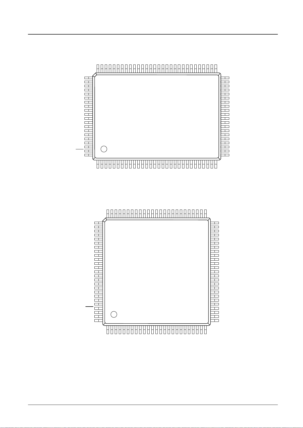
Package Dimensions
unit: mm
3151A-QFP100E
[LC75810E]
23.2
20.0
0.65
[LC75810T]
16.0
14.0
125
0.5
100
(0.58)
3.0max
unit: mm
3274-TQFP100
1.2max
80
81
130
(2.7)
0.1
76
100
(1.0)
(1.0)
0.1
0.2
51
50
14.0
17.2
31
0.3
SANYO: QFP100E
5175
50
14.0
16.0
26
0.8
0.15
0.5
0.125
SANYO: TQFP100
32902RM(OT)No.7141-1/54
Page 2

LC75810E/T
Continued from preceding page.
•
Instruction function
Display on/off control
Smooth up, down, left, and right scrolling of the display
•
Provides a backup function based on power saving mode
•
The frame frequency of the common and segment output
waveforms can be controlled by instructions.
•
Built-in display contrast adjustment circuit
•
Serial data input supports CCB format communication with
the system controller
•
Independent LCD driver block power supply V
•
Provides a
•
RC oscillator circuit
pin for IC internal initialization.
RES
LCD
No.7141-2/54
Page 3
Pin Assignments (Top view)
LC75810E/T
COM10/S79
COM9/S80
COM8
COM7
COM6
COM5
COM4
COM3
COM2
COM1
VDD
VLCD
VLCD0
VLCD1
VLCD2
VLCD3
VSS
OSC
RES
S78
CL
S77
DI
S76
S1
S59
S75
S61
S62
S63
S64
S65
S66
S67
S68
S69
S70
S71
S72
S73
S74
S57
S58
S60
S53
S54
S55
S56
LC75810E
(QFP100E)
S4
S3S9S2
S5
S6
S7
S8
S10
S12
S11
S16
S15
S14
S13
S17
S21
S20
S19
S18
S24
S23
S22
S49
S50
S51
S52
5180
5081
S48
S47
S46
S45
S44
S43
S42
S41
S40
S39
S38
S37
S36
S35
S34
S33
S32
S31
S30
S29CE
31100
301
S25
S28
S27
S26
S51
S52
S53
S54
S56
S57
S58
S59
S61
S62
S63
S64
S65
S66
S67
S68
S69
S70
S71
S72
S73
S74
S76
S77
S78
COM10/S79
COM9/S80
COM8
COM7
COM6
COM5
COM4
COM3
COM2
COM1
VDD
VLCD
VLCD0
VLCD1
VLCD2
VLCD3
VSS
OSC
RES
CE
CL
S75
S1
S2
S3
S4
S5
S6
S7
LC75810T
(TQFP100)
S9
S8
S10
S11
S60
S16
S15
S14
S13
S12
S17
S55
5175
5076
S50
S49
S48
S47
S46
S45
S44
S43
S42
S41
S40
S39
S38
S37
S36
S35
S34
S33
S32
S31
S30
S29
S28
S27
S26DI
26100
251
S22
S21
S20
S19
S18
S25
S24
S23
No.7141-3/54
Page 4
LC75810E/T
Specifications
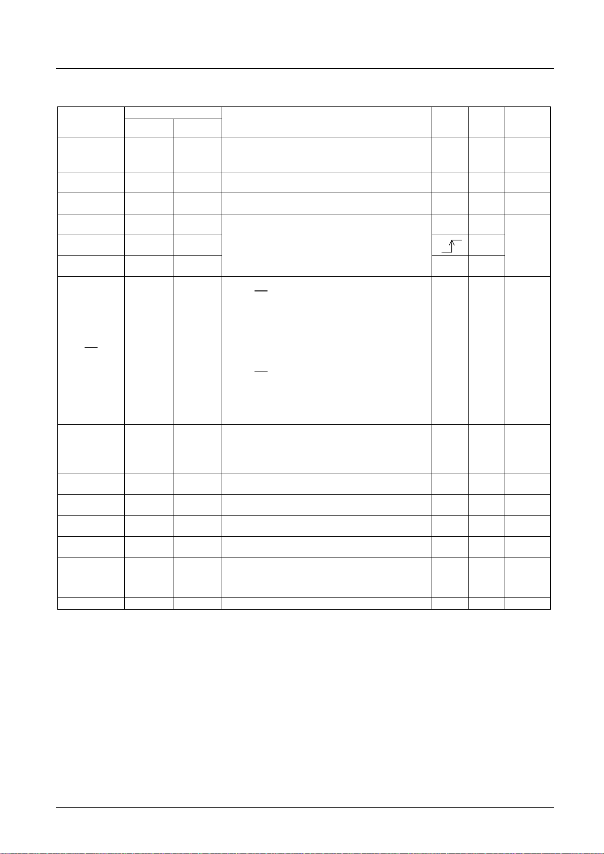
Absolute Maximum Ratings at Ta ==== 25°°°°C, V
Parameter Symbol Conditions Ratings Unit
Maximum supply voltage
Input voltage
Output voltage
Output current
VDD max VDD −0.3 to +7.0
V
max V
LCD
VIN1 CE, CL, DI,
−0.3 to +11.0
LCD
RES
−0.3 to +7.0
VIN2 OSC −0.3 to VDD + 0.3
3 V
V
IN
V
1 OSC −0.3 to V
OUT
V
2 V
OUT
I
1 S1 to S80 300 µA
OUT
I
2 COM1 to COM10 3 mA
OUT
1, V
LCD
LCD
2, V
LCD
LCD
0, S1 to S80, COM1 to COM10 −0.3 to V
Allowable power dissipation Pd max Ta = 85°C 200 mW
Operating temperature Topr −40 to +85 °C
Storage temperature Tstg −55 to +125 °C
Allowable Operating Ranges at Ta ==== −−−−40°°°°C to ++++ 85°°°°C, V
Parameter Symbol Conditions
VDD VDD 2.7 6.0
Supply voltage
V
Output voltage V
V
Input voltage
V
V
Input high level voltage VIH CE, CL, DI,
Input low level voltage VIL CE, CL, DI,
Recommended external
resistance
Recommended external
capacitance
R
C
When the display contrast adjustment circuit is used. 7.0 10.0
LCD
When the display contrast adjustment circuit is not used. 4.5 10.0
0 V
LCD
1 V
LCD
2 V
LCD
3 V
LCD
OSC 10 kΩ
osc
OSC 470 pF
osc
0 4.5 V
LCD
1 3/4 V
LCD
2 2/4 V
LCD
3 1/4 V
LCD
RES
0.8 VDD 6.0 V
RES
0 0.2 VDD V
Guaranteed oscillation range fosc OSC 150 300 600 kHz
Data setup time tds CL, DI (Figure 2) 160 ns
Data hold time tdh CL, DI (Figure 2) 160 ns
CE wait time tcp CE, CL (Figure 2) 160 ns
CE setup time tcs CE, CL (Figure 2) 160 ns
CE hold time tch CE, CL (Figure 2) 160 ns
High level clock pulse width tφH CL (Figure 2) 160 ns
Low level clock pulse width tφL CL (Figure 2) 160 ns
Minimum reset pulse width t
WRES
RES
(Figure 3) 1 µs
==== 0V
SS
3 −0.3 to V
==== 0V
SS
Ratings
min. typ. max.
0 V
LCD
0 V
LCD
0 V
LCD
LCD
LCD
+ 0.3
DD
+ 0.3
+ 0.3
V
LCD
0
LCD
0
LCD
0
LCD
V
V
V
Unit
V
V
No.7141-4/54
Page 5
LC75810E/T
Electrical Characteristics for the Allowable Operating Ranges
Parameter Symbol Conditions
Hysteresis VH CE, CL, DI,
Input high level current IIH CE, CL, DI,
Input low level current IIL CE, CL, DI,
VOH1 S1 to S80: IO = −20 µA
Output high level voltage
V
2 COM1 to COM10: IO = −100 µA
OH
Output low level voltage
Output middle level voltage ∗1
Oscillator frequency f
VOL1 S1 to S80: IO = 20 µA 0.6
2 COM1 to COM10: IO = 100 µA 0.6
V
OL
V
1 S1 to S80: IO = ±20 µA
MID
V
2 COM1 to COM10: IO = ±100 µA
MID
V
3 COM1 to COM10: IO = ±100 µA
MID
R
OSC:
osc
OSC
C
OSC
IDD1 VDD: Power saving mode 5
V
DD
Output open
f
OSC
: Power saving mode 5
LCD
V
LCD
Output open
:
LCD
f
OSC
Current drain
IDD2 VDD:
I
1 V
LCD
I
2 V
LCD
When the display contrast adjustment circuit is used
V
LCD
Output open
I
LCD
3 V
LCD
:
f
OSC
When the display contrast adjustment circuit is not
used
Ratings
min. typ. max.
RES
0.1VDD V
RES
VI = 6.0 V 5.0 µA
:
RES
VI = 0 V −5.0 µA
:
V
LCD
0−0.6
V
LCD
0−0.6
Unit
V
V
2/4 V
= 10 kΩ
= 470 pF
0
LCD
−0.6
3/4 V
0
LCD
−0.6
1/4 V
0
LCD
−0.6
210 300 390 kHz
2/4 V
0
LCD
+0.6
3/4 V
0
LCD
+0.6
1/4 V
LCD
+0.6
V
0
= 6.0 V
700 1400
= 300 kHz
= 10.0 V
= 300 kHz
450 900
µA
= 10.0 V
= 300 kHz
200 400
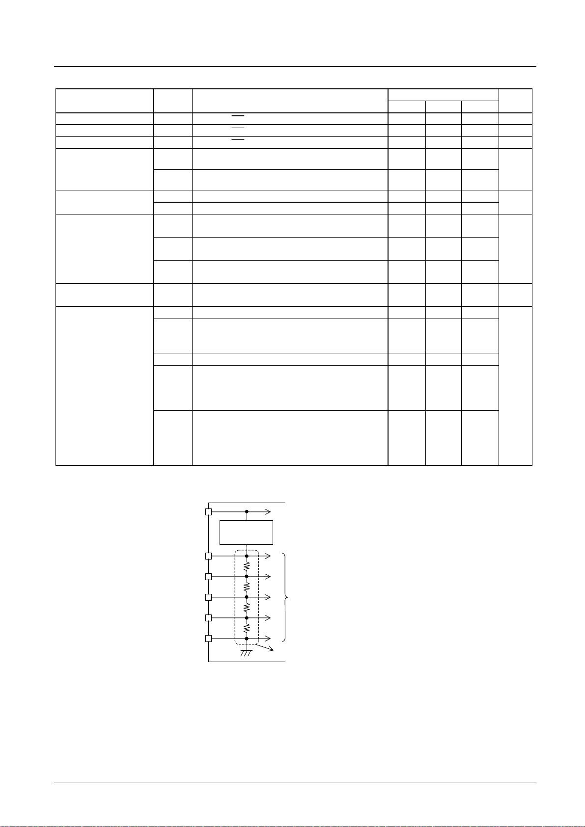
Note ∗1: Excluding the bias voltage generation divider resistors built into the V
V
LCD
CONTRAST
ADJUSTER
0
V
LCD
1
V
LCD
2
V
LCD
V
3
LCD
V
SS
Excluding these resistors
Figure 1
0, V
1, V
2, V
LCD
LCD
LCD
3, and VSS pins. (See figure 1.)
LCD
To the common and segment drivers
No.7141-5/54
Page 6
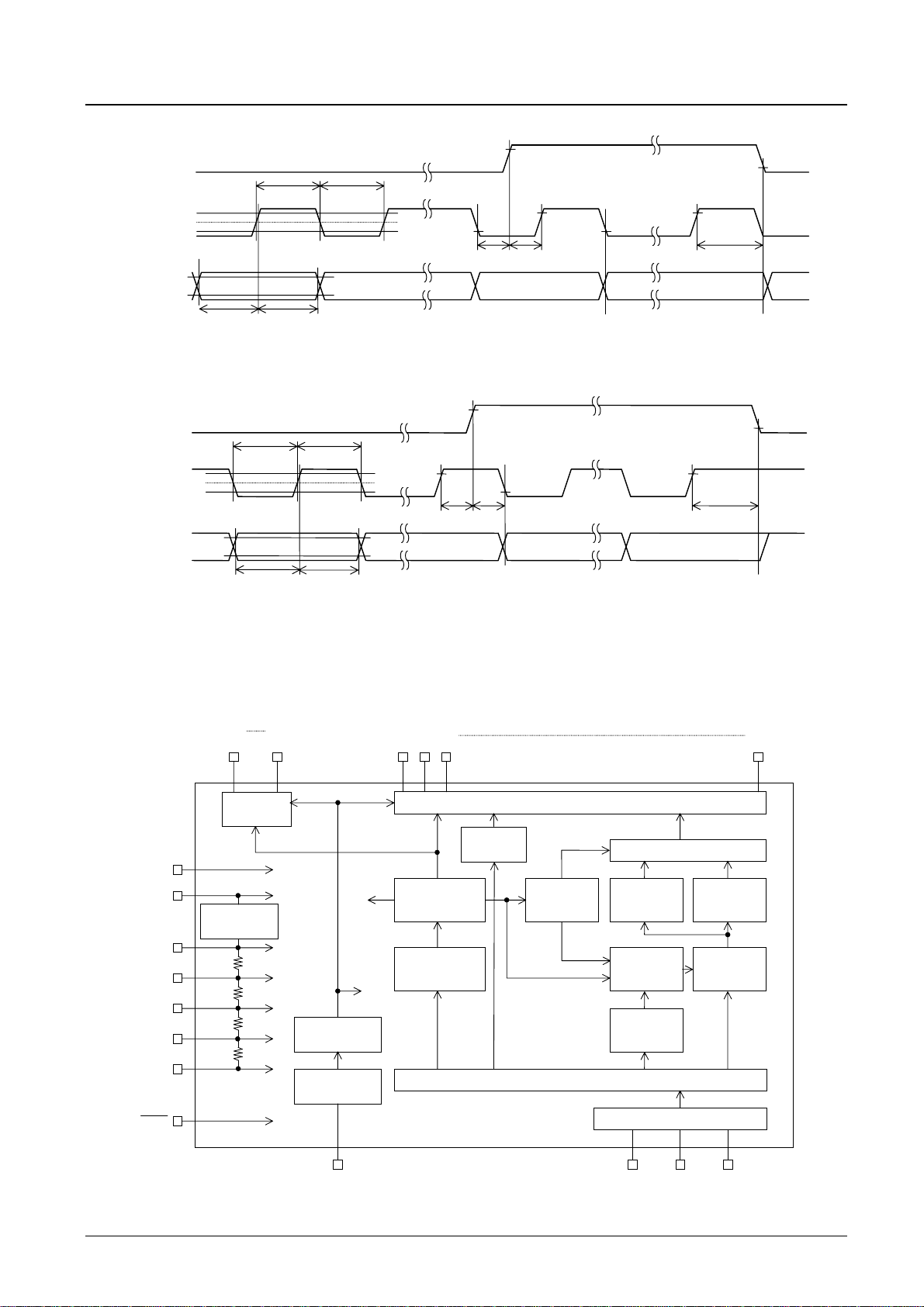
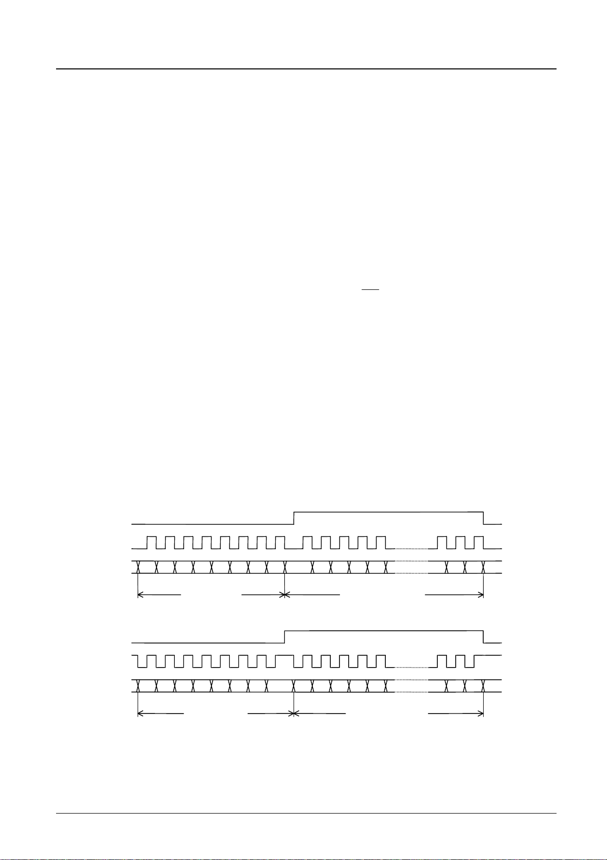
•
When CL is stopped at the low level
CE
LC75810E/T
VIH
VIL
t
φ
H
t
dh
CL
DI
VIH
50%
VIL
VIH
VIL
t
ds
•
When CL is stopped at the high level
CE
φ
L
t
CL
DI
ds
t
t
φ
L
t
t
cs
cp
t
ch
VIH
VIL
φ
H
t
dh
t
VIH
50%
VIL
VIH
VIL
t
t
cs
cp
t
ch
Figure 2
Block Diagram
V
DD
V
LCD
0
V
LCD
1
V
LCD
2
V
LCD
V
3
LCD
V
SS
RES
COM1
COMMON
DRIVER
CONTRAST
ADJUSTER
COM8
TIMING
GENERATOR
CLOCK
GENERATOR
S80/COM9
S78
S79/COM10
ALATCH
INSTRUCTION
DECODER
INSTRUCTION
REGISTER
SEGMENT DRIVER
80bits
SCROLL
COUNTER
SHIFT REGISTER
LATCH
CGRAM
5 × 9 × 16
bits
ADDRESS
COUNTER
ADDRESS
REGISTER
5 × 9 × 240
CCB INTERFACE
S1
CGROM
bits
DCRAM
64 × 8
bits
OSC
DI
CL
CE
No.7141-6/54
Page 7
LC75810E/T
Pin Functions
Pin
S1 to S78
S79/COM10
S80/COM9
Pin No.
LC75810E LC75810T
3 to 80
81
82
1 to 78
79
80
Function
Segment driver outputs
The S79/COM10 and S80/COM9 pins can be used as common
driver outputs under the “set display technique” instruction.
Active
level
I/O
− O OPEN
COM1 to COM8 90 to 83 88 to 81 Common driver outputs − O OPEN
OSC 98 96
CE 100 98 H I
CL 1 99 I
Oscillator connection. An oscillator circuit is formed by connecting
an external resistor and capacitor at this pin.
Serial data transfer inputs. These pins are connected to the
microcontroller.
CE: Chip enable
− I/O VDD
CL: Synchronization clock
DI 2 100
DI: Transfer data
− I
Reset signal input
RES
• When
is low (VSS)
− Display off
RES
99 97
S1 to S78 = “L” (V
S79/COM10 and S80/COM9 = “L” (V
COM1 to COM8 = “L” (V
− Serial data transfer is disabled.
)
SS
)
SS
)
SS
L I GND
− The OSC pin oscillator is stopped.
RES
• When
is high (VDD)
− Display on after a “display on/off control” (display on state
setting) instruction is executed.
− Serial data transfers are enabled.
− The OSC pin oscillator operates.
LCD drive 4/4 bias voltage (high level) supply pin. The level on
this pin can be changed by the display contrast adjustment circuit.
V
0 93 91
LCD
However, V
external power must not be applied to this pin since the pin circuit
0 must be greater than or equal to 4.5 V. Also,
LCD
− O OPEN
includes the display contrast adjustment circuit.
V
1 94 92
LCD
V
2 95 93
LCD
V
3 96 94
LCD
VDD 91 89
LCD drive 3/4 bias voltage (middle level) supply pin. This pin can
be used to supply the 3/4 V
0 voltage level externally.
LCD
LCD drive 2/4 bias voltage (middle level) supply pin. This pin can
be used to supply the 2/4 V
0 voltage level externally.
LCD
LCD drive 1/4 bias voltage (middle level) supply pin. This pin can
be used to supply the 1/4 V
0 voltage level externally.
LCD
Logic block power supply connection. Provide a voltage of
between 2.7 and 6.0 V.
− I OPEN
− I OPEN
− I OPEN
− − −
LCD driver block power supply connection. Provide a voltage of
V
92 90
LCD
between 7.0 and 10.0 V when the display contrast adjustment
circuit is used and provide a voltage of between 4.5 and 10.0 V
− − −
when the circuit is not used.
VSS 97 95 Power supply connection. Connect to ground. − − −
Handling
when
unused
GND
No.7141-7/54
Page 8
LC75810E/T
Block Functions
•
AC (Address counter)
AC is a counter that provides the DCRAM address.
The address is automatically modified internally, and the LCD display state is retained.
•
DCRAM (Data control RAM)
DCRAM is the RAM that is used to store display data expressed as 8-bit character codes. (These character codes are
converted to 5 × 7, 5 × 8, or 5 × 9 dot matrix character patterns using CGROM or CGRAM.)
DCRAM has a capacity of 64 × 8 bits, and can hold 64 characters. The table below lists the correspondence between the
6-bit DCRAM address loaded into AC and the display position on the LCD panel.
•
For a 64 digits × 1 line display structure (For a “set display technique” instruction with 0Z1 = 0 and 0Z2 = 0)
When the DCRAM address loaded into AC is 00H
Display digit 1 2 3 4 5 6 7 8 9 10 11 12 13 14 15 16 17 18 61 62 63 64
DCRAM address
(hexadecimal)
First line 00 01 02 03 04 05 06 07 08 09 0A 0B 0C 0D 0E 0F 10 11 3C 3D 3E 3F
However, when the display smooth scrolling is performed, the DCRAM address shifts as follows.
Display digit 1 2 3 4 5 6 7 8 9 10 11 12 13 14 15 16 17 18 61 62 63 64
DCRAM address
(hexadecimal)
First line 01 02 03 04 05 06 07 08 09 0A 0B 0C 0D 0E 0F 10 11 12 3D 3E 3F 00
Shift to the left
by 1 character
digit
Display digit 1 2 3 4 5 6 7 8 9 10 11 12 13 14 15 16 17 18 61 62 63 64
DCRAM address
(hexadecimal)
First line 3F 00 01 02 03 04 05 06 07 08 09 0A 0B 0C 0D 0E 0F 10 3B 3C 3D 3E
Shift to the right
by 1 character
digit
Note that the display area on the LCD is display digits 1 to 16 on the first line when a display technique is 5 × 7, 5 × 8,
or 5 × 9 dots, and it is display digits 1 to 13 on the first line when a display technique is 6 × 7, 6 × 8, or 6 × 9 dots.
•
For a 32 digits × 2 lines display structure (For a “set display technique” instruction with 0Z1 = 1 and 0Z2 = 0)
When the DCRAM address loaded into AC is 00H
Display digit 1 2 3 4 5 6 7 8 9 10 11 12 13 14 15 16 17 18 29 30 31 32
DCRAM address
(hexadecimal)
First line 00 01 02 03 04 05 06 07 08 09 0A 0B 0C 0D 0E 0F 10 11 1C 1D 1E 1F
Second line 20 21 22 23 24 25 26 27 28 29 2A 2B 2C 2D 2E 2F 30 31 3C 3D 3E 3F
However, when the display smooth scrolling is performed, the DCRAM address shifts as follows.
Display digit 1 2 3 4 5 6 7 8 9 10 11 12 13 14 15 16 17 18 29 30 31 32
DCRAM address
(hexadecimal)
First line 01 02 03 04 05 06 07 08 09 0A 0B 0C 0D 0E 0F 10 11 12 1D 1E 1F 00
Second line 21 22 23 24 25 26 27 28 29 2A 2B 2C 2D 2E 2F 30 31 32 3D 3E 3F 20
Shift to the left
by 1 character
digit
Display digit 1 2 3 4 5 6 7 8 9 10 11 12 13 14 15 16 17 18 29 30 31 32
DCRAM address
(hexadecimal)
First line 1F 00 01 02 03 04 05 06 07 08 09 0A 0B 0C 0D 0E 0F 10 1B 1C 1D 1E
Second line 3F 20 21 22 23 24 25 26 27 28 29 2A 2B 2C 2D 2E 2F 30 3B 3C 3D 3E
Shift to the right
by 1 character
digit
Display digit 1 2 3 4 5 6 7 8 9 10 11 12 13 14 15 16 17 18 29 30 31 32
DCRAM address
(hexadecimal)
First line 20 21 22 23 24 25 26 27 28 29 2A 2B 2C 2D 2E 2F 30 31 3C 3D 3E 3F
Second line 00 01 02 03 04 05 06 07 08 09 0A 0B 0C 0D 0E 0F 10 11 1C 1D 1E 1F
Shift to the up or
down by 1
character digit
Note that the display area on the LCD is display digits 1 to 16 on the first line when a display technique is 5 × 7, 5 × 8,
or 5 × 9 dots, and it is display digits 1 to 13 on the first line when a display technique is 6 × 7, 6 × 8, or 6 × 9 dots.
No.7141-8/54
Page 9
LC75810E/T
•
For a 16 digits × 4 lines display structure (For a “set display technique” instruction with 0Z1 = 0 and 0Z2 = 1)
When the DCRAM address loaded into AC is 00H
DCRAM address (hexadecimal)
Display digit 1 2 3 4 5 6 7 8 9 10 11 12 13 14 15 16
First line 00 01 02 03 04 05 06 07 08 09 0A 0B 0C 0D 0E 0F
Second line 10 11 12 13 14 15 16 17 18 19 1A 1B 1C 1D 1E 1F
Third line 20 21 22 23 24 25 26 27 28 29 2A 2B 2C 2D 2E 2F
Fourth line 30 31 32 33 34 35 36 37 38 39 3A 3B 3C 3D 3E 3F
However, when the display smooth scrolling is performed, the DCRAM address shifts as follows.
DCRAM address (hexadecimal)
Display digit 1 2 3 4 5 6 7 8 9 10 11 12 13 14 15 16
First line 01 02 03 04 05 06 07 08 09 0A 0B 0C 0D 0E 0F 00
Second line 11 12 13 14 15 16 17 18 19 1A 1B 1C 1D 1E 1F 10
Third line 21 22 23 24 25 26 27 28 29 2A 2B 2C 2D 2E 2F 20
Fourth line 31 32 33 34 35 36 37 38 39 3A 3B 3C 3D 3E 3F 30
Shift to the left by
1 character digit
Display digit 1 2 3 4 5 6 7 8 9 10 11 12 13 14 15 16
DCRAM address (hexadecimal)
First line 0F 00 01 02 03 04 05 06 07 08 09 0A 0B 0C 0D 0E
Second line 1F 10 11 12 13 14 15 16 17 18 19 1A 1B 1C 1D 1E
Third line 2F 20 21 22 23 24 25 26 27 28 29 2A 2B 2C 2D 2E
Fourth line 3F 30 31 32 33 34 35 36 37 38 39 3A 3B 3C 3D 3E
Shift to the right by
1 character digit
Display digit 1 2 3 4 5 6 7 8 9 10 11 12 13 14 15 16
First line 10 11 12 13 14 15 16 17 18 19 1A 1B 1C 1D 1E 1F
DCRAM address (hexadecimal)
Second line 20 21 22 23 24 25 26 27 28 29 2A 2B 2C 2D 2E 2F
Third line 30 31 32 33 34 35 36 37 38 39 3A 3B 3C 3D 3E 3F
Fourth line 00 01 02 03 04 05 06 07 08 09 0A 0B 0C 0D 0E 0F
Shift to the up by 1 character digit
Display digit 1 2 3 4 5 6 7 8 9 10 11 12 13 14 15 16
First line 30 31 32 33 34 35 36 37 38 39 3A 3B 3C 3D 3E 3F
DCRAM address (hexadecimal)
Second line 00 01 02 03 04 05 06 07 08 09 0A 0B 0C 0D 0E 0F
Third line 10 11 12 13 14 15 16 17 18 19 1A 1B 1C 1D 1E 1F
Fourth line 20 21 22 23 24 25 26 27 28 29 2A 2B 2C 2D 2E 2F
Shift to the down by 1 character digit
Note that the display area on the LCD is display digits 1 to 16 on the first line when a display technique is 5 × 7, 5 × 8,
or 5 × 9 dots, and it is display digits 1 to 13 on the first line when a display technique is 6 × 7, 6 × 8, or 6 × 9 dots.
Note ∗2: The DCRAM address is expressed in hexadecimal.
Least significant bit
↓
LSB MSB
DCRAM address DA0 DA1 DA2 DA3 DA4 DA5
Most significant bit
↓
Hexadecimal Hexadecimal
Example: When the DCRAM address is 2EH
DA0 DA1 DA2 DA3 DA4 DA5
0 1 1 1 0 1
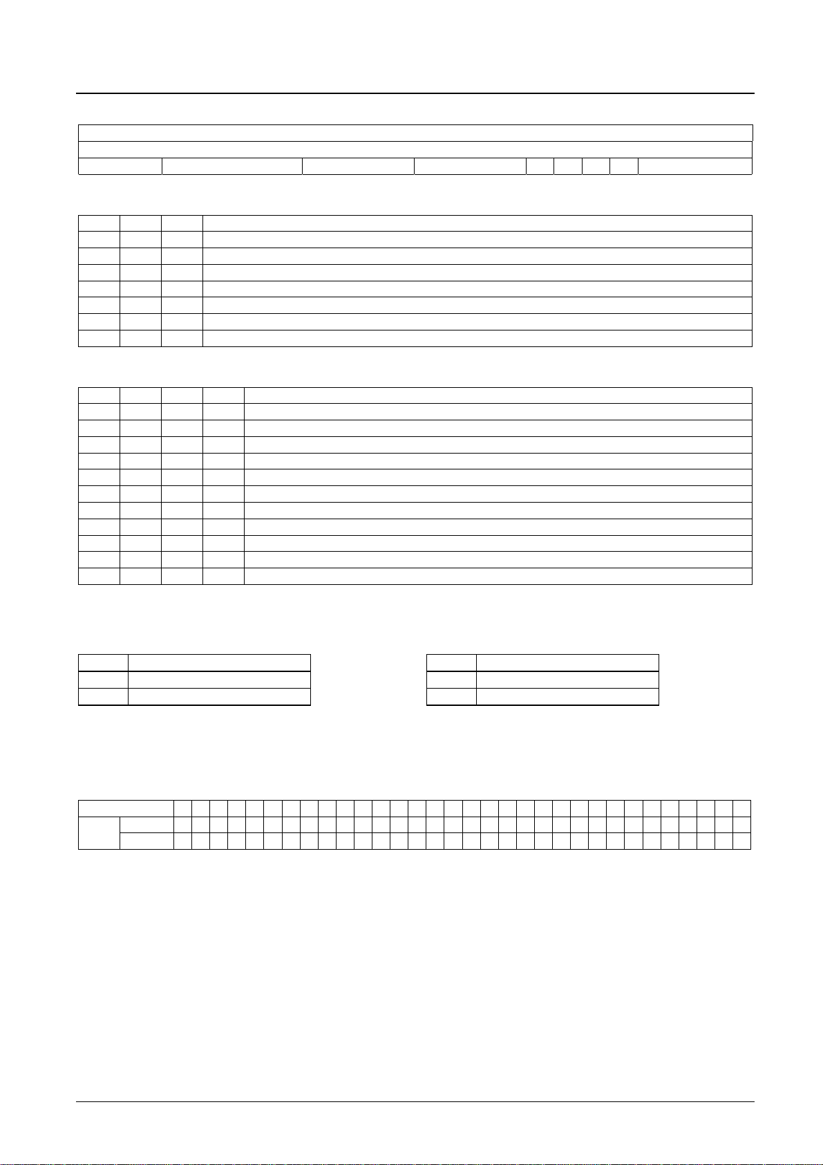
Note ∗3: 5 × 7 dots
5 × 8 dots
5 × 9 dots
6 × 7 dots
6 × 8 dots
6 × 9 dots
• • •
16-digit display 5 × 7 dots.
• • •
16-digit display 4 × 8 dots.
• • •
16-digit display 3 × 9 dots.
• • •
13-digit display 6 × 7 dots.
• • •
13-digit display 6 × 8 dots.
• • •
13-digit display 6 × 9 dots.
No.7141-9/54
Page 10
LC75810E/T
3
2
3
2
•
CGROM (Character generator ROM)
CGROM is the ROM that is used to generate the 240 kinds of 5 × 7, 5 × 8, or 5 × 9 dot matrix character patterns from
the 8-bit character codes. CGROM has a capacity of 240 × 45 bits. When a character code is written to DCRAM, the
character pattern stored in the CGROM corresponding to the character code is displayed at the position on the LCD
corresponding to the DCRAM address loaded into AC.
•
CGRAM (Character generator RAM)
CGRAM is the RAM to which user programs can freely write arbitrary character patterns. Up to 16 kinds of 5 × 7, 5 ×
8, or 5 × 9 dot matrix character patterns can be stored. CGRAM has a capacity of 16 × 45 bits.
•
ALATCH (Additional data latch)
ALATCH is the latch that is used to store the ADATA display data for the accessory display. ALATCH has a capacity
of 80 bits, and the stored display data is displayed directly without the use of CGROM or CGRAM.
•
SC (Scroll counter)
SC is the counter that is used to scroll the display in the left, right, up, or down directions in dot units. Since this
function scrolls in dot units, it implements smooth scrolling.
Reset Function
The LC75810E and LC75810T are reset when a low level is applied to the
pin at power on and, in normal mode. On a
RES
reset the LC75810E and LC75810T create a display with all LCD panels turned off. However, after a reset applications
must set the contents of DCRAM, ALATCH, and CGRAM before turning on display with a “display on/off control”
instruction since the contents of these memories are undefined. That is, applications must execute the following
instructions.
• Set display technique
• DCRAM data write
• ALATCH data write (If ALATCH is used.)
• CGRAM data write (IF CGRAM is used.)
• Set AC and SC addresses
• Set display contrast (If the display contrast adjustment circuit is used.)
After executing the above instructions, applications must turn on the display with a “display on/off control” instruction.
Note that when applications turn off in the normal mode, applications must turn off the display with a “display on/off
control” instruction. (See the detailed instruction descriptions.)
Serial Data Transfer Format
•
When CL is stopped at the low level
CE
CL
D14
DI
B1
B0
•
When CL is stopped at the high level
1110D0D1
CCB address
8 bits
1000
D4D3D2
A3A2A1A0B3B2
Instruction data
Up to 144 bits
D14
CE
CL
D14
DI
B0
B1
•
CCB address: 4EH
•
D0 to D143: Instruction data
CCB address
8 bits
00011110
D0 D1
D4D3D2
A3A2A1A0B3B2
Instruction data
Up to 144 bits
D14
The data is acquired on the rising edge of the CL signal and latched on the falling edge of the CE signal. When
transferring instruction data from the microcontroller, applications must assure that the time from the transfer of one
set of instruction data until the next instruction data transfer is significantly longer than the instruction execution time.
No.7141-10/54
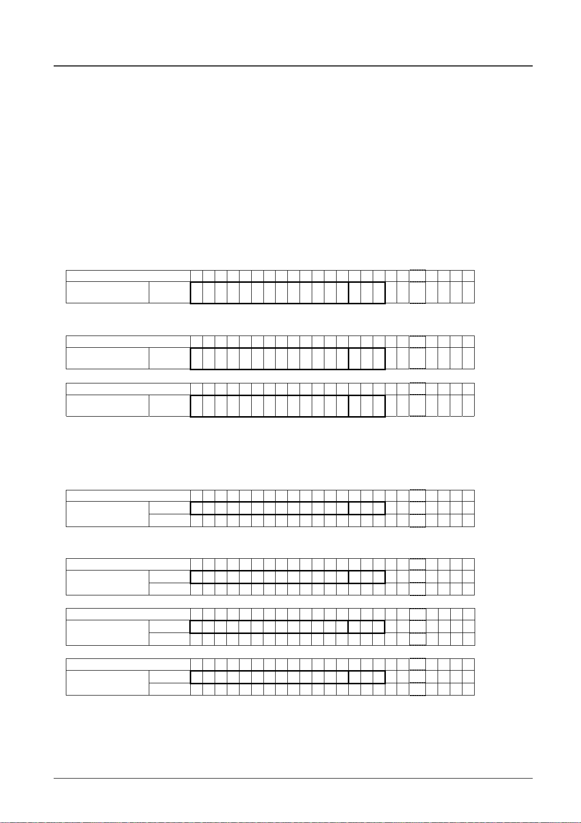
Page 11
LC75810E/T
s
s
s
µ
0
1
0
0
0
0
FC
DT2
DT1
X
X
X
X
X
DW
OZ2
OZ1
technique
Set display
µ
5)
∗
(
s/27
s/162
µ
µ
0
27
0
1
0
0
BU
SC
A
M
DG16
DG15
DG14
DG13
DG12
DG11
DG10
DG9
DG8
DG7
DG6
DG5
DG4
DG3
DG2
DG1
control
Display on/off
1
1
0
0
0
X
D/U
R/L
X
X
X
X
VS3
VS2
VS1
VS0
X
X
X
X
X
HS2
HS1
HS0
Display scroll
6)
∗
(
4)
∗
time (
Execution
D143
D142
D141
D140
D139
D138
D137
D136
D135
D134
D133
D132
D131
D130
D129
D128
D127
D126
D125
D124
D123
D122
D121
D120
D119
D118
D117
D116
D115
D114
D113
D112
D111
•
•
•
D81
D80
D79
•
•
•
D57
D56
D55
•
•
•
D1D0Instruction
Instruction Table
µ
Set AC and SC
s
µ
27
0
0
1
0
0
X
X
X
X
X
DA5
DA4
DA3
DA2
DA1
DA0
X
X
X
X
VA3
VA2
VA1
VA0
X
X
X
X
X
HA2
HA1
HA0
addresses
s
µ
s/ti
µ
27
DCRAM data
1
0
1
0
0
X
IM2
IM1
X
X
DA5
DA4
DA3
DA2
DA1
DA0
AC7
AC6
AC5
AC4
AC3
AC2
AC1
AC0
8)
∗
(
7)
∗
write (
s
µ
s
µ
0
s/40.5
µ
27
0
1
1
0
0
X
X
X
AD80
AD79
AD78
AD77
AD76
AD75
AD74
AD73
AD72
AD71
AD70
AD69
AD68
AD67
AD66
AD65
AD64
AD63
AD62
AD61
AD60
AD59
AD58
AD57
AD56
•
•
•
AD26
AD25
AD24
•
•
•
AD2
AD1
write
CGRAM data
ALATCH data
•
•
•
1
1
1
0
0
X
X
WM
CA7
CA6
CA5
CA4
CA3
CA2
CA1
CA0
X
X
X
CD45
CD44
CD43
CD42
CD41
CD40
CD39
CD38
CD37
CD36
CD35
CD34
CD33
CD32
CD2
CD1
10)
(
9)
write (
s
µ
∗
0
X: don’t care
0
0
0
1
0
X
X
CTC
X
X
X
X
CT3
CT2
CT1
CT0
s
µ
58
=
300
210
×
s
µ
300 kHz).
=
s 40.5
µ
1.43
×
ti
=
300
210
×
s
µ
s ti
300 kHz. The execution times differ when the oscillator frequency fosc differs.
=
4: The execution times listed here apply when fosc
∗
contrast
Set display
∗
Notes
µ
232
=
300
×
s
µ
210 kHz
s 162
=
µ
39
=
300
×
s
µ
Example: When fosc
27
210
210
300 kHz) if another “display scroll” instruction is executed immediately after a preceding “display scroll” instruction.
=
1) is set, the execution time is 27 µs (when fosc
=
5: Note that when the power saving mode (BU
6: The execution time must be seen as being 162 µs (when fosc
∗
∗
1).
=
0) or super-increment mode (IM1 = 0, IM2
=
1, IM2
=
8: Note that the data format differs when a “DCRAM data write” instruction is executed in normal increment mode (IM1
∗
7,
∗
300 kHz) if a “DCRAM data write” instruction is executed in super-increment mode. (See detailed instruction descriptions.)
=
Also note that the execution time is ti µs (when fosc
300 kHz)
=
1). Also note that the execution time is 40.5 µs (when fosc
=
if a “CGRAM data write” instruction is executed in double write mode. (See detailed instruction descriptions.)
10: Note that the data format differs when a “CGRAM data write” instruction is executed in double write mode (WM
∗
9,
∗
No.7141-11/54
Page 12
LC75810E/T
Detailed Instruction Descriptions
•
Set display technique
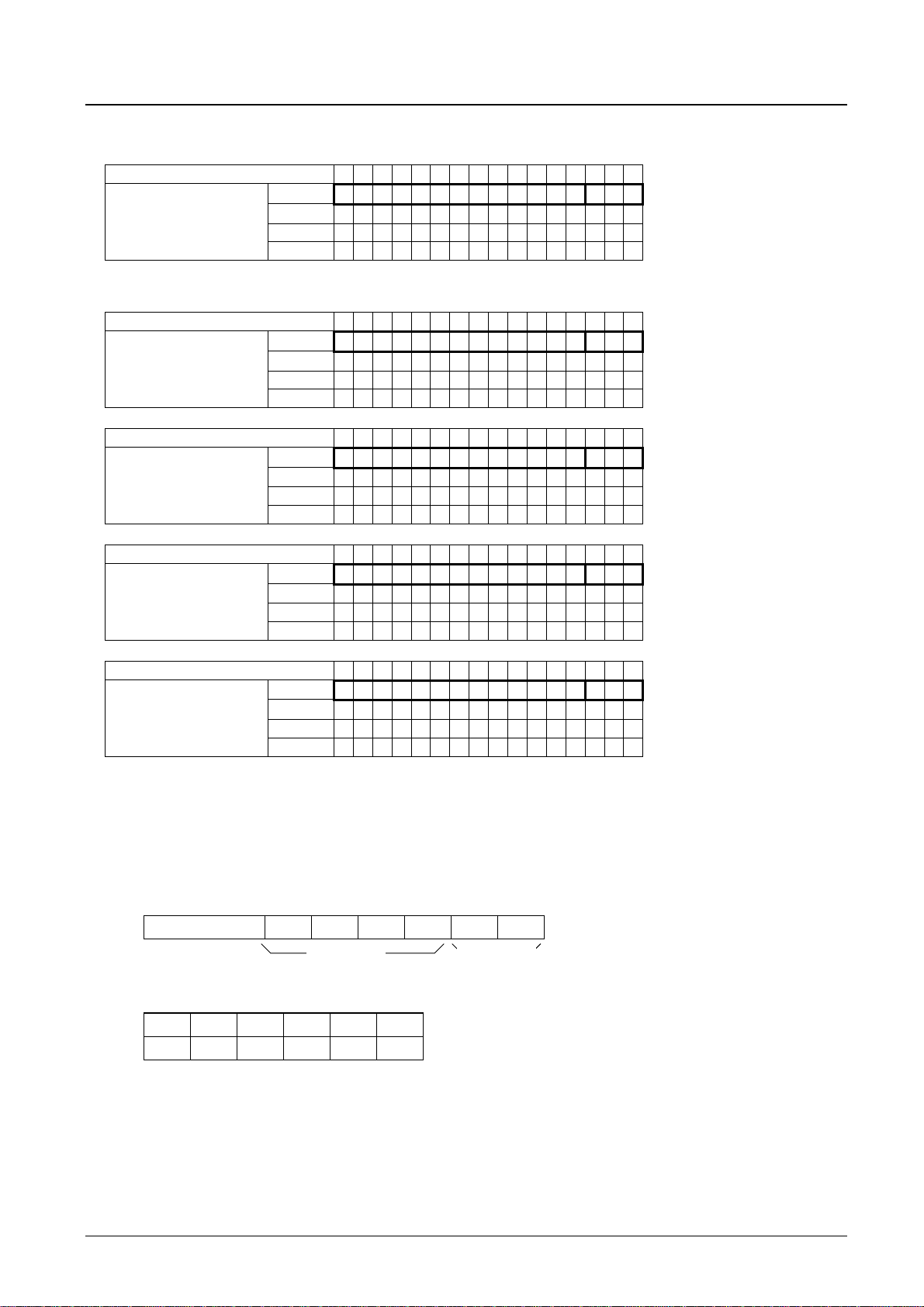
D128 D129 D130 D131 D132 D133 D134 D135 D136 D137 D138 D139 D140 D141 D142 D143
OZ1 OZ2 DW X X X X X DT1 DT2 FC 0 0 0 0 1
DT1, DT2: Set the display technique
DT1 DT2 Display technique
0 0 1/8 duty, 1/4 bias drive S80 S79
1 0 1/9 duty, 1/4 bias drive COM9 S79
0 1 1/10 duty, 1/4 bias drive COM9 COM10
• • •
<Sets the display technique.>
Code
X:don’t care
Output pins
S80/COM9 S79/COM10
∗11: Sn (n = 79, 80): Segment output
COMn (n = 9, 10): Common output
FC: Set the frame frequency of the common and segment output waveforms
FC
1/8 duty, 1/4 bias drive f8[Hz] 1/9 duty, 1/4 bias drive f9[Hz] 1/10 duty, 1/4 bias drive f10[Hz]
0
1
fosc
3072
fosc
1536
Frame frequency
fosc
3456
fosc
1728
fosc
3840
fosc
1920
OZ1, OZ2: Set the display structure
OZ1 OZ2 Display structure
0 0 64 digits × 1 line display structure
1 0 32 digits × 2 lines display structure
0 1 16 digits × 4 lines display structure
∗12: See block functions (DCRAM)
DW: Set the dot font width
DW Dot font width Number of display digits
0 5-dot font width 16 digits × 1 line (5 × 7 dots), 15 digits × 1 line (5 × 8 or 5 × 9 dots)
1 6-dot font width 13 digits × 1 line (6 × 7, 6 × 8, or 6 × 9 dots)
•
∗13:
5-dot font width (5 × 7, 5 × 8, or 5 × 9 dots)
COM1
COM2
COM3
COM4
COM5
COM6
COM7
COM8
S80/COM9
S79/COM10
S1S2S3S4S5S6S7S8S9
•
6-dot font width (6 × 7, 6 × 8, or 6 × 9 dots)
COM1
COM2
COM3
COM4
COM5
COM6
COM7
COM8
S80/COM9
S79/COM10
S1S2S3S4S5S6S7S8S9
S10
S10
S11
S12
S67
S71
S68
S72
S69
S73
S70
S74
S71
S75
S72
S73
S76
S74
S77
S75
S78
S76
COM10/S79
S77
COM9/S80
S78
No.7141-12/54
Page 13
LC75810E/T
•
Display on/off control
D120 D121 D122 D123 D124 D125 D126 D127 D128 D129 D130 D131 D132 D133 D134 D135 D136 D137 D138 D139 D140 D141 D142 D143
DG1 DG2 DG3 DG4 DG5 DG6 DG7 DG8 DG9
• • •
<Turns the display on or off.>
DG10 DG11 DG12 DG13 DG14 DG15 DG1
Code
M A SC BU 0 0 1 0
6
M, A: Specifies the data to be turned on or off.
M A Display operating state
0 0 Both MDATA and ADATA are turned off. (The display is forcibly turned off, regardless of the DG1 to DG16 data.)
0 1 Only ADATA is turned on. (The ADATA of display digits specified by the DG1 to DG16 data are turned on.)
1 0 Only MDATA is turned on. (The MDATA of display digits specified by the DG1 to DG16 data are turned on.)
1 1 Both MDATA and ADATA are turned on. (The MDATA and ADATA of display digits specified by the DG1 to DG16 data are turned on.)
*14: MDATA, ADATA
5 × 7 dot matrix 5 × 8 dot matrix 5 × 9 dot matrix
• • • • •
• • •
ADATA
MDATA
• • • • •
• • •
ADATA
MDATA
• • • • •
• • •
ADATA
MDATA
6 × 7 dot matrix 6 × 8 dot matrix 6 × 9 dot matrix
• • • • •
• • •
ADATA
MDATA
• • • • •
• • •
ADATA
MDATA
• • • • •
• • •
ADATA
MDATA
DG1 to DG16: Specifies the display digit.
Display digit 1 2 3 4 5 6 7 8 9 10 11 12 13 14 15 16
Display digit data DG1 DG2 DG3 DG4 DG5 DG6 DG7 DG8 DG9 DG10 DG11 DG12 DG13 DG14 DG15 DG16
For example, if DG1 to DG8 are 1, and DG9 to DG16 are 0, then display digits 1 to 8 will be turned on, and display digits
9 to 16 will be turned off (blanked).
SC: Controls the common and segment output pins.
SC Common and segment output pin states
0 Output of LCD drive waveforms
1 Fixed at the VSS level (all segments off)
Note ∗15: When SC is 1, the S1 to S80 and COM1 to COM10 output pins are set to the VSS level, regardless of the M, A, and DG1 to DG16 data.
BU: Controls the normal mode and power saving mode.
BU Mode
0 Normal mode
Power saving mode
(In this mode, the OSC pin oscillator is stopped, and the common and segment pins are set to the V
1
the “display on/off control” and “set display contrast” instructions cannot be executed. Thus applications must set the IC to normal mode before
executing any of the other instructions.)
level. In this mode, instructions other than
SS
No.7141-13/54
Page 14
LC75810E/T
•
Display scroll
D120 D121 D122 D123 D124 D125 D126 D127 D128 D129 D130 D131 D132 D133 D134 D135 D136 D137 D138 D139 D140 D141 D142 D143
HS0 HS1 HS2 X X X X X VS0 VS1 VS2 VS3 X X X X R/L D/U X 0 0 0 1 1
HS0 to HS2: Set the amount of smooth scrolling to be applied to MDATA in the left/right direction.
HS0 HS1 HS2 Amount of smooth scrolling to be applied to MDATA in the left/right direction
0 0 0 No shift in either the left or right direction
1 0 0 Shift 1 dot to the left or right. (The shift direction (left or right) is specified with the R/L data.)
0 1 0 Shift 2 dots to the left or right. (The shift direction (left or right) is specified with the R/L data.)
1 1 0 Shift 3 dots to the left or right. (The shift direction (left or right) is specified with the R/L data.)
0 0 1 Shift 4 dots to the left or right. (The shift direction (left or right) is specified with the R/L data.)
1 0 1 Shift 5 dots to the left or right. (The shift direction (left or right) is specified with the R/L data.)
0 1 1 Shift 6 dots to the left or right. (The shift direction (left or right) is specified with the R/L data.)
• • •
<Scrolls the display smoothly.>
Code
X: don’t care
VS0 to VS3: Set the amount of smooth scrolling to be applied to MDATA in the up/down direction.
VS0 VS1 VS2 VS3 Amount of smooth scrolling to be applied to MDATA in the up/down direction
0 0 0 0 No shift in either the up or down direction
1 0 0 0 Shift 1 dot to the up or down. (The shift direction (up or down) is specified with the D/U data.)
0 1 0 0 Shift 2 dots to the up or down. (The shift direction (up or down) is specified with the D/U data.)
1 1 0 0 Shift 3 dots to the up or down. (The shift direction (up or down) is specified with the D/U data.)
0 0 1 0 Shift 4 dots to the up or down. (The shift direction (up or down) is specified with the D/U data.)
1 0 1 0 Shift 5 dots to the up or down. (The shift direction (up or down) is specified with the D/U data.)
0 1 1 0 Shift 6 dots to the up or down. (The shift direction (up or down) is specified with the D/U data.)
1 1 1 0 Shift 7 dots to the up or down. (The shift direction (up or down) is specified with the D/U data.)
0 0 0 1 Shift 8 dots to the up or down. (The shift direction (up or down) is specified with the D/U data.)
1 0 0 1 Shift 9 dots to the up or down. (The shift direction (up or down) is specified with the D/U data.) (∗16)
0 1 0 1 Shift 10 dots to the up or down. (The shift direction (up or down) is specified with the D/U data.) (∗17)
Notes: ∗16: This shift cannot be used when MDATA is 5 × 7 or 6 × 7 dots.
∗17: This shift cannot be used when MDATA is 5 × 7, 5 × 8, 6 × 7 or 6 × 8 dots.
R/L: Specifies the MDATA shift direction (left or right). D/U: Specifies the MDATA shift direction (up or down).
R/L MDATA shift direction (left or right) D/U MDATA shift direction (up or down)
0 Shift left 0 Shift up
1 Shift right
1 Shift down
∗18 Example of the “display scroll” instruction execution
Assume that a 32 digits × 2 lines display structure (OZ1 = 1, OZ2 = 0) has been set up with the “set display technique”
instruction, and that the following data has been written to DCRAM with the “DCRAM data write” instruction.
Display digit 1 2 3 4 5 6 7 8 9 10 11 12 13 14 15 16 17 18 19 20 21 22 23 24 25 26 27 28 29 30 31 32
DCRAM
First line A B C D E F G H I J K L M N O P Q R S T U V W X Y Z < > z y x w
data
Second line 0 1 2 3 4 5 6 7 8 9 a b c d e f g h i j k l m n o p q r s t u v
No.7141-14/54
Page 15
•
Display state (1)
With no shifting in any direction, left, right, up, or down.
HS0 HS1 HS2 VS0 VS1 VS2 VS3 R/L D/U
0 0 0 0 0 0 0 X X
X: don’t care
(5 × 7 dot matrix)
(6 × 7 dot matrix)
LC75810E/T
•
Display state (2)
Shifted 3 dots to the left relative to display state (1)
HS0 HS1 HS2 VS0 VS1 VS2 VS3 R/L D/U
1 1 0 0 0 0 0 0 0
(5 × 7 dot matrix)
(6 × 7 dot matrix)
•
Display state (3)
Shifted 6 dots to the left relative to display state (1) Shifted 3 dots to the left relative to display state (2)
HS0 HS1 HS2 VS0 VS1 VS2 VS3 R/L D/U HS0 HS1 HS2 VS0 VS1 VS2 VS3 R/L D/U
0 1 1 0 0 0 0 0 0 1 1 0 0 0 0 0 0 0
(5 × 7 dot matrix)
(6 × 7 dot matrix)
No.7141-15/54
Page 16
•
Display state (4)
Shifted 4 dots to the up relative to display state (1)
HS0 HS1 HS2 VS0 VS1 VS2 VS3 R/L D/U
0 0 0 0 0 1 0 0 0
(5 × 7 dot matrix)
(6 × 7 dot matrix)
LC75810E/T
•
Display state (5)
Shifted 8 dots to the up relative to display state (1) Shifted 4 dots to the up relative to display state (4)
HS0 HS1 HS2 VS0 VS1 VS2 VS3 R/L D/U HS0 HS1 HS2 VS0 VS1 VS2 VS3 R/L D/U
0 0 0 0 0 0 1 0 0 0 0 0 0 0 1 0 0 0
(5 × 7 dot matrix)
(6 × 7 dot matrix)
•
Display state (6)
Shifted 3 dots to the left and 4 dots to the up relative to display state (1)
HS0 HS1 HS2 VS0 VS1 VS2 VS3 R/L D/U
1 1 0 0 0 1 0 0 0
(5 × 7 dot matrix)
(6 × 7 dot matrix)
No.7141-16/54
Page 17
LC75810E/T
•
Display state (7)
Shifted 6 dots to the left and 8 dots to the up relative Shifted 8 dots to the up relative to display state (3)
to display state (1)
HS0 HS1 HS2 VS0 VS1 VS2 VS3 R/L D/U HS0 HS1 HS2 VS0 VS1 VS2 VS3 R/L D/U
0 1 1 0 0 0 1 0 0 0 0 0 0 0 0 1 0 0
Shifted 6 dots to the left relative to display state (5) Shifted 3 dots to the left and 4 dots to the up relative
HS0 HS1 HS2 VS0 VS1 VS2 VS3 R/L D/U HS0 HS1 HS2 VS0 VS1 VS2 VS3 R/L D/U
0 1 1 0 0 0 0 0 0 1 1 0 0 0 1 0 0 0
to display state (6)
(5 × 7 dot matrix)
(6 × 7 dot matrix)
•
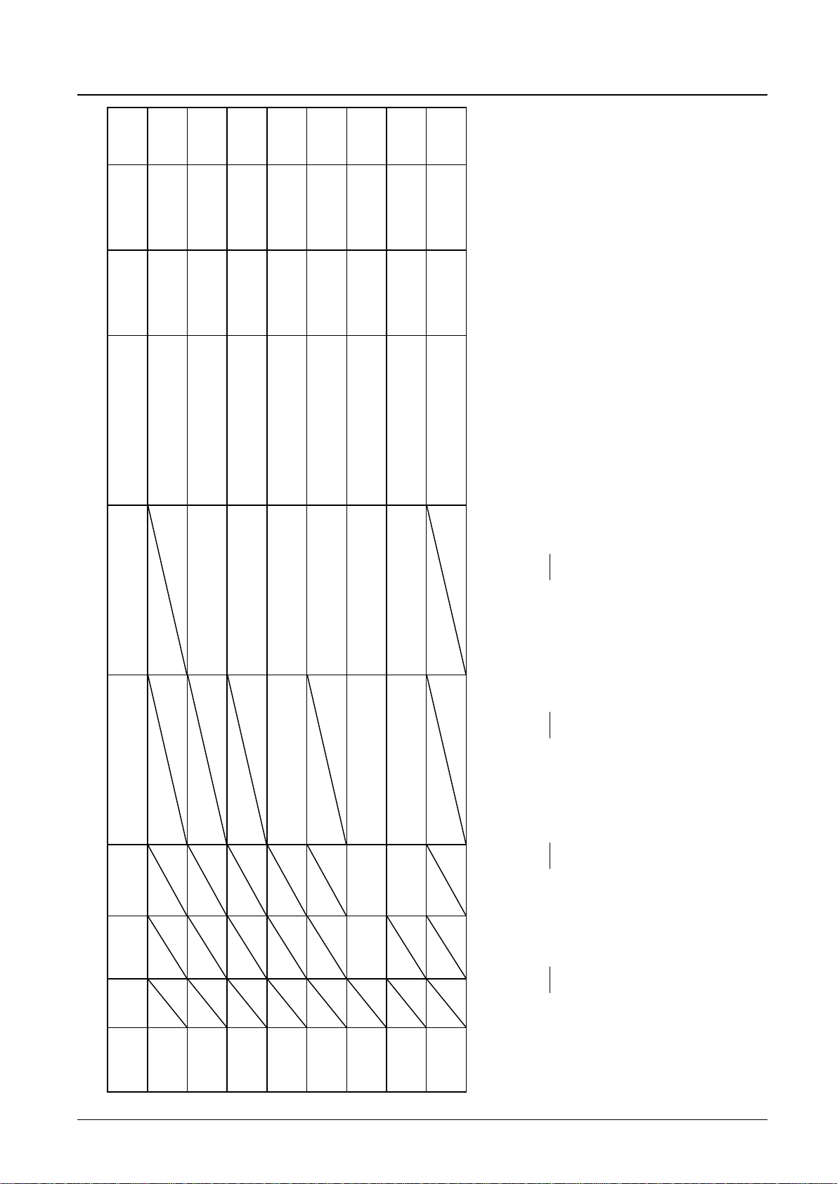
Set AC and SC addresses
pattern for SC.>
D112 D113 D114 D115 D116 D117 D118 D119 D120 D121 D122 D123 D124 D125 D126 D127
HA0 HA1 HA2 X X X X X VA0 VA1 VA2 VA3 X X X X
• • •
<Specifies the DCRAM address for AC and the dot address of the dot matrix character
Code
Code
D128 D129 D130 D131 D132 D133 D134 D135 D136 D137 D138 D139 D140 D141 D142 D143
DA0 DA1 DA2 DA3 DA4 DA5 X X X X X 0 0 1 0 0
DA0 to DA5: DCRAM address
DA0 DA1 DA2 DA3 DA4 DA5
LSB
MSB
↑ ↑
Least Most
significant bit significant bit
HA0 to HA2: Dot address in the horizontal direction for the dot matrix character pattern
HA0 HA1 HA2
LSB MSB
↑ ↑
Least Most
significant bit significant bit
VA0 to VA3: Dot address in the vertical direction for the dot matrix character pattern
VA0 VA1 VA2 VA3
LSB MSB
↑ ↑
Least Most
significant bit significant bit
X: don’t care
No.7141-17/54
Page 18

LC75810E/T
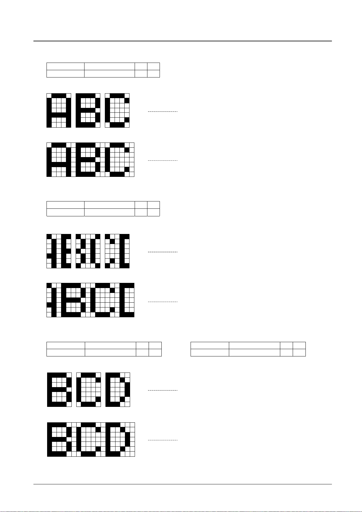
∗19 The figure below lists the correspondence between the data HA0 to HA2 which is dot address in the horizontal
direction and the dot matrix character pattern, and the correspondence between the data VA0 to VA3 which is dot
address in the vertical direction and the dot matrix character pattern.
•
5-dot font width: 5 × 7, 5 × 8, or 5 × 9 dots
Dot address in the
horizontal direction
HA0 to HA2 (HEX)
0 1 2 3 4 5
• The area at HA0 to 2 = 5H is allocated to the space at the right of
the dot matrix character pattern.
• The area at VA0 to 3 = 7H, for 5
7 dot characters, is allocated to
×
the space at the bottom of the dot matrix character pattern.
• The area at VA0 to 3 = 8H is illegal for 5
8 dot characters, it is allocated to the space at the bottom of the
×
7 dot characters. For 5
×
dot matrix character pattern.
• The area at VA0 to 3 = 9H is illegal for 5 × 7 or 5 × 8 dot
characters. For 5 × 9 dot characters, it is allocated to the space at
the bottom of the dot matrix character pattern.
Dot address in
the vertical
direction
VA0 to
VA3
(HEX)
0
1
2
3
4
5
6
7
8
9
•
6-dot font width: 6 × 7, 6 × 8, or 6 × 9 dots
Dot address in the
horizontal direction
HA0 to HA2 (HEX)
0 1 2 3 4 5
• The area at HA0 to 2 = 5H is allocated to the space at the right of
the dot matrix character pattern.
• The area at VA0 to 3 = 7H, for 6
7 dot characters, is allocated to
×
the space at the bottom of the dot matrix character pattern.
• The area at VA0 to 3 = 8H is illegal for 6
8 dot characters, it is allocated to the space at the bottom of the
×
7 dot characters. For 6
×
dot matrix character pattern.
• The area at VA0 to 3 = 9H is illegal for 6
characters. For 6
9 dot characters, it is allocated to the space at
×
×
7 or 6
×
8 dot
the bottom of the dot matrix character pattern.
Dot address in
the vertical
direction
VA0 to
VA3
(HEX)
0
1
2
3
4
5
6
7
8
9
∗20: Example of the “set AC and SC addresses” instruction execution
Assume that a 32 digits × 2 lines display structure (OZ1 = 1, OZ2 = 0) has been set up with the “set display technique”
instruction, and that the following data has been written to DCRAM with the “DCRAM data write” instruction.
DCRAM
Display digit 1 2 3 4 5 6 7 8 9 10 11 12 13 14 15 16
First line (DCRAM
address (hexadecimal)) A (00) B (01) C (02) D (03) E (04) F (05) G (06) H (07) I (08) J (09) K (0A) L (0B) M (0C) N (0D) O (0E) P (0F)
data
Second line (DCRAM
address (hexadecimal)) 0 (20) 1 (21) 2 (22) 3 (23) 4 (24) 5 (25) 6 (26) 7 (27) 8 (28) 9 (29) a (2A) b (2B) c (2C) d (2D) e (2E) f (2F)
Display digit 17 18 19 20 21 22 23 24 25 26 27 28 29 30 31 32
DCRAM
data
First line (DCRAM
address (hexadecimal))
Second line (DCRAM
address (hexadecimal)) g (30) h (31) i (32) j (33) k (34) l (35) m (36) n (37) o (38) p (39) q (3A) r (3B) s (3C) t (3D) u (3E) v (3F)
Q
(10)
R
(11)
S
(12)
T
(13)
U
(14)
V
(15)
W
(16)
X
Y
(17)
(18) Z (19) < (1A) > (1B) z (1C) y (1D) x (1E) w (1F)
No.7141-18/54
Page 19

LC75810E/T
•
When DA0 to 5 is set to 07H, HA0 to 2 is set to 0H, and VA0 to 3 is set to 0H.
HA0 HA1 HA2 VA0 VA1 VA2 VA3 DA0 DA1 DA2 DA3 DA4 DA5
0 0 0 0 0 0 0 1 1 1 0 0 0
(5 × 7 dot matrix)
(6 × 7 dot matrix)
•
When DA0 to 5 is set to 09H, HA0 to 2 is set to 4H, and VA0 to 3 is set to 0H.
HA0 HA1 HA2 VA0 VA1 VA2 VA3 DA0 DA1 DA2 DA3 DA4 DA5
0 0 1 0 0 0 0 1 0 0 1 0 0
(5 × 7 dot matrix)
(6 × 7 dot matrix)
•
When DA0 to 5 is set to 0FH, HA0 to 2 is set to 0H, and VA0 to 3 is set to 3H.
HA0 HA1 HA2 VA0 VA1 VA2 VA3 DA0 DA1 DA2 DA3 DA4 DA5
0 0 0 1 1 0 0 1 1 1 1 0 0
(5 × 7 dot matrix)
(6 × 7 dot matrix)
No.7141-19/54
Page 20

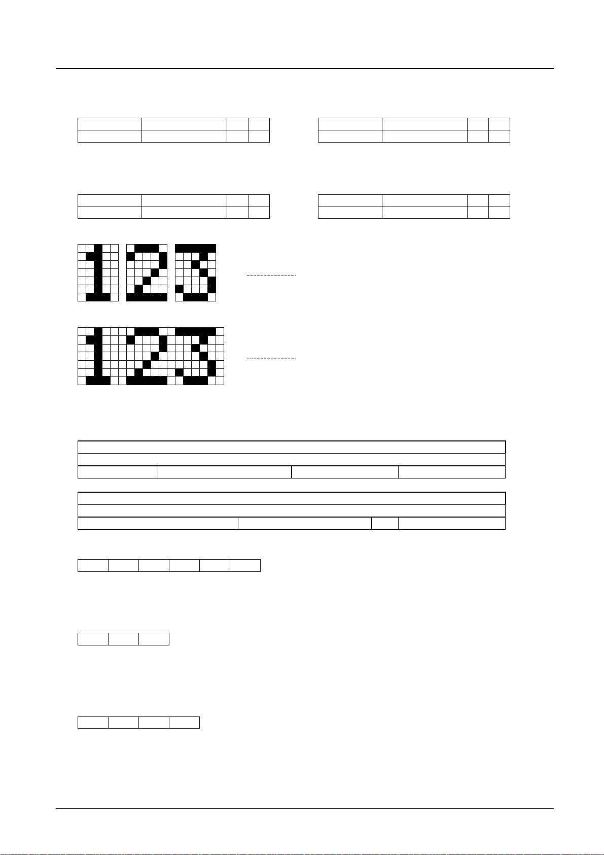
LC75810E/T
•
When DA0 to 5 is set to 14H, HA0 to 2 is set to 1H, and VA0 to 3 is set to 2H.
HA0 HA1 HA2 VA0 VA1 VA2 VA3 DA0 DA1 DA2 DA3 DA4 DA5
1 0 0 0 1 0 0 0 0 1 0 1 0
(5 × 7 dot matrix)
(6 × 7 dot matrix)
•
When DA0 to 5 is set to 34H, HA0 to 2 is set to 3H, and VA0 to 3 is set to 6H.
HA0 HA1 HA2 VA0 VA1 VA2 VA3 DA0 DA1 DA2 DA3 DA4 DA5
1 1 0 0 1 1 0 0 0 1 0 1 1
(5 × 7 dot matrix)
(6 × 7 dot matrix)
•
DCRAM data write
D120 D121 D122 D123 D124 D125 D126 D127 D128 D129 D130 D131 D 132 D133 D134 D135 D136 D137 D138 D139 D140 D141 D142 D143
AC0 AC1 AC2 AC3 AC4 AC5 AC6 AC7 DA0 DA1 DA2 DA3 DA4 DA5 X X IM1 IM2 X 0 0 1 0 1
DA0 to DA5: DCRAM address
DA0 DA1 DA2 DA3 DA4 DA5
LSB MSB
• • •
<Specifies the DCRAM address and stores data at that address.>
Code
X: don’t care
↑ ↑
Least significant bit Most significant bit
AC0 to AC7: DCRAM data (character code)
AC0 AC1 AC2 AC3 AC4 AC5 AC6 AC7
LSB MSB
↑ ↑
Least significant bit Most significant bit
This instruction writes the 8 bits of data AC0 to AC7 to DCRAM. This data is a character code, and is converted to a 5 × 7,
5 × 8, or 5 × 9 dot matrix display data using CGROM or CGRAM.
No.7141-20/54
Page 21

LC75810E/T
IM1 and IM2: Sets the method of writing data to DCRAM
IM1 IM2 DCRAM data write method
0 0 Normal DCRAM data write (Specifies the DCRAM address and writes the DCRAM data.)
1 0 Normal increment mode DCRAM data write (Increments the DCRAM address by +1 each time data is written to DCRAM.)
0 1 Super-increment mode DCRAM data write (Writes 2 to 16 characters of DCRAM data in a single operation.)
•
∗21
DCRAM data write method when IM1 is 0 and IM2 is 0.
CE
CCB addressCCB address CCB addressCCB address
DI
DCRAM
(1)
Instruction
execution
time (27 µs)
DCRAM data
write finishes
Instruction
execution
time (27 µs)
DCRAM data
write finishes
Instruction
execution
time (27 µs)
DCRAM data
write finishes
24 bits24 bits24 bits24 bits
Instruction
execution
time (27 µs)
•
DCRAM data write method when IM1 is 1 and IM2 is 0.
(Instructions other than the “DCRAM data write” instruction cannot be executed.)
CE
CCB addressCCB address CCB addr ess CCB address CCB address CCB address
DCRAM
DI
(2)
Instruction
execution
time (27 µs)
DCRAM data
write finishes
8 bits 8 bits8 bits24 bits
Instruction
execution
time (27 µs)
Instruction
execution
time (27 µs)
DCRAM data
write finishes
DCRAM data
write finishes
Instruction
execution
time (27 µs)
Instruction
execution
time (27 µs)
DCRAM data
write finishes
8 bits
DCRAM data
write finishes
(4)(3)(3)(3)(3)
16 bits
Instruction
execution
time (27 µs)
(1)(1)(1)
DCRAM data
write finishes
DCRAM data
write finishes
(Instructions other than the “DCRAM data write” instruction cannot be executed.)
•
DCRAM data write method when IM1 is 0 and IM2 is 1.
CE
CCB address
DI
DCRAM
ti = 13.5µs × ( -1) (n = 8m + 16, m is an integer between 2 and 16 that is the number of characters written as DCRAM
data.)
n
8
(5)
Instruction
execution
time (ti µs)
CCB address
DCRAM data
write finishes
(5)
n bit
Instruction
execution
time (ti µs)
DCRAM data
write finishes
CCB address
(5)
n bitn bit
Instruction
execution
time (ti µs)
DCRAM data
write finishes
For example When n = 32 bits (m = 2): ti = 40.5 µs (when fosc = 300 kHz)
When n = 80 bits (m = 8): ti = 121.5 µs (when fosc = 300 kHz)
When n = 144 bits (m = 16): ti = 229.5 µs (when fosc = 300 kHz)
Note that the instruction execution time of 27 µs and ti values in µs apply when fosc = 300 kHz, and that these times will
differ when the oscillator frequency fosc differs.
No.7141-21/54
Page 22

LC75810E/T
Data format (1) (24 bits)
Code
D120 D121 D122 D123 D124 D125 D126 D127 D128 D129 D130 D131 D132 D133 D134 D135 D136 D137 D138 D139 D140 D141 D142 D143
AC0 AC1 AC2 AC3 AC4 AC5 AC6 AC7 DA0 DA1 DA2 DA3 DA4 DA5 X X 0 0 X 0 0 1 0 1
X: don’t care
Data format (2) (24 bits)
Code
D120 D121 D122 D123 D124 D125 D126 D127 D128 D129 D130 D131 D132 D133 D134 D135 D136 D137 D138 D139 D140 D141 D142 D143
AC0 AC1 AC2 AC3 AC4 AC5 AC6 AC7 DA0 DA1 DA2 DA3 DA4 DA5 X X 1 0 X 0 0 1 0 1
X: don’t care
Data format (3) (8 bits)
Code
D136 D137 D138 D139 D140 D141 D142 D143
AC0 AC1 AC2 AC3 AC4 AC5 AC6 AC7
Data format (4) (16 bits)
Code
D128 D129 D130 D131 D132 D133 D134 D135 D136 D137 D138 D139 D140 D141 D142 D143
AC0 AC1 AC2 AC3 AC4 AC5 AC6 AC7 0 0 X 0 0 1 0 1
X:don’t care
Data format (5) (n bits)
Code
Dz Dz+1 Dz+2 Dz+3 Dz+4 Dz+5 Dz+6 Dz+7
AC01 AC11 AC21 AC31 AC41 AC51 AC61 AC71
⋅⋅⋅⋅⋅⋅⋅⋅⋅⋅⋅⋅⋅⋅⋅⋅⋅⋅⋅⋅⋅
⋅⋅⋅⋅⋅⋅⋅⋅⋅⋅⋅⋅⋅⋅⋅⋅⋅⋅⋅⋅⋅
D112 D113 D114 D115 D116 D117 D118 D119
AC0
AC1
AC2
AC3
AC4
AC5
AC6
m-1
m-1
m-1
m-1
m-1
m-1
AC7
m-1
m-1
Code
D120 D121 D122 D123 D124 D125 D126 D127 D128 D129 D130 D131 D132 D133 D134 D135 D136 D137 D138 D139 D140 D141 D142 D143
AC0m AC1m AC2m AC3m AC4m AC5m AC6m AC7m DA01 DA11 DA21 DA31 DA41 DA51 X X 0 1 X 0 0 1 0 1
X: don’t care
Here, n = 8m + 16, z = 128 - 8m (m is an integer between 2 and 16 that is the number of characters written as DCRAM
data.)
Correspondence between the DCRAM address and the DCRAM data
DCRAM address DCRAM data
DA01 to DA51 AC01 to AC71
(DA01 to DA51) + 1 AC02 to AC72
(DA01 to DA51) + 2 AC03 to AC73
(DA01 to DA51) + (m − 3) AC0
(DA01 to DA51) + (m − 2) AC0
(DA01 to DA51) + (m − 1) AC0m to AC7m
m-2
m-1
to AC7
to AC7
m-2
m-1
No.7141-22/54
Page 23

LC75810E/T
Example 1: When n = 32 bits (m = 2: 2 characters DCRAM data write operation)
D112 D113 D114 D115 D116 D117 D118 D119 D120 D121 D122 D123 D124 D125 D126 D127
AC01 AC11 AC21 AC31 AC41 AC51 AC61 AC71 AC02 AC12 AC22 AC32 AC42 AC52 AC62 AC72
Code
Code
D128 D129 D130 D131 D132 D133 D134 D135 D136 D137 D138 D139 D140 D141 D142 D143
DA01 DA11 DA21 DA31 DA41 DA51 X X 0 1 X 0 0 1 0 1
X: don’t care
Correspondence between the DCRAM address and the DCRAM data
DCRAM address DCRAM data
DA01 to DA51 AC01 to AC71
(DA01 to DA51) + 1 AC02 to AC72
Example 2: When n = 80 bits (m = 8: 8 characters DCRAM data write operation)
D64 D65 D66 D67 D68 D69 D70 D71 D72 D73 D74 D75 D76 D77 D78 D79
AC01 AC11 AC21 AC31 AC41 AC51 AC61 AC71 AC02 AC12 AC22 AC32 AC42 AC52 AC62 AC72
Code
Code
D80 D81 D82 D83 D84 D85 D86 D87 D88 D89 D90 D91 D92 D93 D94 D95
AC03 AC13 AC23 AC33 AC43 AC53 AC63 AC73 AC04 AC14 AC24 AC34 AC44 AC54 AC64 AC74
Code
D96 D97 D98 D99 D100 D101 D102 D103 D104 D105 D106 D107 D108 D109 D110 D111
AC05 AC15 AC25 AC35 AC45 AC55 AC65 AC75 AC06 AC16 AC26 AC36 AC46 AC56 AC66 AC76
Code
D112 D113 D114 D115 D116 D117 D118 D119 D120 D121 D122 D123 D124 D125 D126 D127
AC07 AC17 AC27 AC37 AC47 AC57 AC67 AC77 AC08 AC18 AC28 AC38 AC48 AC58 AC68 AC78
Code
D128 D129 D130 D131 D132 D133 D134 D135 D136 D137 D138 D139 D140 D141 D142 D143
DA01 DA11 DA21 DA31 DA41 DA51 X X 0 1 X 0 0 1 0 1
X: don’t care
Correspondence between the DCRAM address and the DCRAM data
DCRAM address DCRAM data
DA01 to DA51 AC01 to AC71
(DA01 to DA51) + 1 AC02 to AC72
(DA01 to DA51) + 2 AC03 to AC73
(DA01 to DA51) + 3 AC04 to AC74
(DA01 to DA51) + 4 AC05 to AC75
(DA01 to DA51) + 5 AC06 to AC76
(DA01 to DA51) + 6 AC07 to AC77
(DA01 to DA51) + 7 AC08 to AC78
No.7141-23/54
Page 24

LC75810E/T
Example 3: When n = 144 bits (m = 16: 16 characters DCRAM data write operation)
D0 D1 D2 D3 D4 D5 D6 D7 D8 D9 D10 D11 D12 D13 D14 D15
AC00 AC10 AC20 AC30 AC40 AC50 AC60 AC70 AC01 AC11 AC21 AC31 AC41 AC51 AC61 AC71
Code
Code
D16 D17 D18 D19 D20 D21 D22 D23 D24 D25 D26 D27 D28 D29 D30 D31
AC03 AC13 AC23 AC33 AC43 AC53 AC63 AC73 AC04 AC14 AC24 AC34 AC44 AC54 AC64 AC74
Code
D32 D33 D34 D35 D36 D37 D38 D39 D40 D41 D42 D43 D44 D45 D46 D47
AC05 AC15 AC25 AC35 AC45 AC55 AC65 AC75 AC06 AC16 AC26 AC36 AC46 AC56 AC66 AC76
Code
D48 D49 D50 D51 D52 D53 D54 D55 D56 D57 D58 D59 D60 D61 D62 D63
AC07 AC17 AC27 AC37 AC47 AC57 AC67 AC77 AC08 AC18 AC28 AC38 AC48 AC58 AC68 AC78
Code
D64 D65 D66 D67 D68 D69 D70 D71 D72 D73 D74 D75 D76 D77 D78 D79
AC09 AC19 AC29 AC39 AC49 AC59 AC69 AC79 AC010 AC110 AC210 AC310 AC410 AC510 AC610 AC710
Code
D80 D81 D82 D83 D84 D85 D86 D87 D88 D89 D90 D91 D92 D93 D94 D95
AC011 AC111 AC211 AC311 AC411 AC511 AC611 AC711 AC012 AC112 AC212 AC312 AC412 AC512 AC612 AC712
Code
D96 D97 D98 D99 D100 D101 D102 D103 D104 D105 D106 D107 D108 D109 D110 D111
AC013 AC113 AC213 AC313 AC413 AC513 AC613 AC713 AC014 AC114 AC214 AC314 AC414 AC514 AC614 AC714
Code
D112 D113 D114 D115 D116 D117 D118 D119 D120 D121 D122 D123 D124 D125 D126 D127
AC015 AC115 AC215 AC315 AC415 AC515 AC615 AC715 AC016 AC116 AC216 AC316 AC416 AC516 AC616 AC716
Code
D128 D129 D130 D131 D132 D133 D134 D135 D136 D137 D138 D139 D140 D141 D142 D143
DA01 DA11 DA21 DA31 DA41 DA51 X X 0 1 X 0 0 1 0 1
X: don’t care
Correspondence between the DCRAM address and the DCRAM data
DCRAM address DCRAM data DCRAM address DCRAM data
DA01 to DA51 AC01 to AC71 (DA01 to DA51) + 8 AC09 to AC79
(DA01 to DA51) + 1 AC02 to AC72 (DA01 to DA51) + 9 AC010 to AC710
(DA01 to DA51) + 2 AC03 to AC73 (DA01 to DA51) + 10 AC011 to AC711
(DA01 to DA51) + 3 AC04 to AC74 (DA01 to DA51) + 11 AC012 to AC712
(DA01 to DA51) + 4 AC05 to AC75 (DA01 to DA51) + 12 AC013 to AC713
(DA01 to DA51) + 5 AC06 to AC76 (DA01 to DA51) + 13 AC014 to AC714
(DA01 to DA51) + 6 AC07 to AC77 (DA01 to DA51) + 14 AC015 to AC715
(DA01 to DA51) + 7 AC08 to AC78
(DA01 to DA51) + 15 AC016 to AC716
No.7141-24/54
Page 25

LC75810E/T
•
ALATCH data write
D56 D57 D58 D59 D60 D61 D62 D63 D64 D65 D66 D67 D68 D69 D70 D71
AD1 AD2 AD3 AD4 AD5 AD6 AD7 AD8 AD9 AD10 AD11 AD12 AD13 AD14 AD15 AD16
• • • • •
<Write data to the ALATCH>
Code
Code
D72 D73 D74 D75 D76 D77 D78 D79 D80 D81 D82 D83 D84 D85 D86 D87
AD17 AD18 AD19 AD20 AD21 AD22 AD23 AD24 AD25 AD26 AD27 AD28 AD29 AD30 AD31 AD32
Code
D88 D89 D90 D91 D92 D93 D94 D95 D96 D97 D98 D99 D100 D101 D102 D103
AD33 AD34 AD35 AD36 AD37 AD38 AD39 AD40 AD41 AD42 AD43 AD44 AD45 AD46 AD47 AD48
Code
D104 D105 D106 D107 D108 D109 D110 D111 D112 D113 D114 D115 D116 D117 D118 D119
AD49 AD50 AD51 AD52 AD53 AD54 AD55 AD56 AD57 AD58 AD59 AD60 AD61 AD62 AD63 AD64
Code
D120 D121 D122 D123 D124 D125 D126 D127 D128 D129 D130 D131 D132 D133 D134 D135
AD65 AD66 AD67 AD68 AD69 AD70 AD71 AD72 AD73 AD74 AD75 AD76 AD77 AD78 AD79 AD80
Code
D136 D137 D138 D139 D140 D141 D142 D143
X X X 0 0 1 1 0
X: don’t care
AD1 to AD80: ADATA display data
In addition to the 5 × 7, 5 × 8, 5 × 9, 6 × 7, 6 × 8, or 6 × 9 dot matrix display data (MDATA), the LC75810E/T also supports
an accessory display of 5 or 6 segments (ADATA) at each display digit, and allows arbitrary data to be displayed directly
without going through CGROM or CGRAM. The figure below shows the correspondence between that data and the
display. When ADn = 1 (where n is an integer between 1 and 80), the segment corresponding to that data will be turned on.
5-dot font width (5 × 7, 5 × 8, or 5 × 9 dots)
COM1
COM2
COM3
COM4
COM5
COM6
COM7
COM8
S80/COM9
S79/COM10
S1S2S3S4S5
S6S7S8
S9
AD76 AD77 AD78 AD79 AD80AD2AD1 AD3 AD4 AD5 AD7 AD8 AD9 AD10AD6 AD72AD71 AD73 AD74 AD75
S71
S72
S73
S74
S75
S76
S77
S10
S78
COM9/S80
COM10/S79
No.7141-25/54
Page 26

6-dot font width (6 × 7, 6 × 8, or 6 × 9 dots)
LC75810E/T
COM1
AD6 AD12 AD72 AD78
AD73 AD74 AD75 AD76 AD77AD2AD1 AD3 AD4 AD5 AD8 AD9 AD10 AD11AD7 AD68AD6 7 AD6 9 AD70 AD71
COM2
COM3
COM4
COM5
COM6
COM7
COM8
S80/COM9
S79/COM10
S1S2S3S4S5S6S7S8S9
S10
S11
S12
S67
S68
S69
S70
S71
S72
S73
S74
S75
S76
Correspondence between ADATA and the output pins
ADATA Corresponding output pin ADATA Corresponding output pin ADATA Corresponding output pin
AD1 S1 AD31 S31 AD61 S61
AD2 S2 AD32 S32 AD62 S62
AD3 S3 AD33 S33 AD63 S63
AD4 S4 AD34 S34 AD64 S64
AD5 S5 AD35 S35 AD65 S65
AD6 S6 AD36 S36 AD66 S66
AD7 S7 AD37 S37 AD67 S67
AD8 S8 AD38 S38 AD68 S68
AD9 S9 AD39 S39 AD69 S69
AD10 S10 AD40 S40 AD70 S70
AD11 S11 AD41 S41 AD71 S71
AD12 S12 AD42 S42 AD72 S72
AD13 S13 AD43 S43 AD73 S73
AD14 S14 AD44 S44 AD74 S74
AD15 S15 AD45 S45 AD75 S75
AD16 S16 AD46 S46 AD76 S76
AD17 S17 AD47 S47 AD77 S77
AD18 S18 AD48 S48 AD78 S78
AD19 S19 AD49 S49 AD79 S79
AD20 S20 AD50 S50
AD21 S21 AD51 S51
AD22 S22 AD52 S52
AD23 S23 AD53 S53
AD24 S24 AD54 S54
AD25 S25 AD55 S55
AD26 S26 AD56 S56
AD27 S27 AD57 S57
AD28 S28 AD58 S58
AD29 S29 AD59 S59
AD30 S30
AD60 S60
AD80 S80
S77
S78
No.7141-26/54
Page 27

LC75810E/T
•
CGRAM data write
D80 D81 D82 D83 D84 D85 D86 D87 D88 D89 D90 D91 D92 D93 D94 D95
CD1 CD2 CD3 CD4 CD5 CD6 CD7 CD8 CD9 CD10 CD11 CD12 CD13 CD14 CD15 CD16
• • • • •
<Specifies the CGRAM address and stores data at that address.>
Code
Code
D96 D97 D98 D99 D100 D101 D102 D103 D104 D105 D106 D107 D108 D109 D110 D111
CD17 CD18 CD19 CD20 CD21 CD22 CD23 CD24 CD25 CD26 CD27 CD28 CD29 CD30 CD31 CD32
Code
D112 D113 D114 D115 D116 D117 D118 D119 D120 D121 D122 D123 D124 D125 D126 D127
CD33 CD34 CD35 CD36 CD37 CD38 CD39 CD40 CD41 CD42 CD43 CD44 CD45 X X X
Code
D128 D129 D130 D131 D132 D133 D134 D135 D136 D137 D138 D139 D140 D141 D142 D143
CA0 CA1 CA2 CA3 CA4 CA5 CA6 CA7 WM X X 0 0 1 1 1
X:don’t care
CA0 to CA7: CGRAM address
CA0 CA1 CA2 CA3 CA4 CA5 CA6 CA7
LSB MSB
↑ ↑
Least significant bit Most significant bit
CD1 to CD45: CGRAM data (5 × 7, 5 × 8, or 5 × 9 dot matrix display data)
The bit CDn (where n is an integer between 1 and 45) corresponds to the 5 × 7, 5 × 8, or 5 × 9 dot matrix display data.
The figure below shows that correspondence. When CDn is 1, the dots which correspond to that data will be turned on.
CD1 CD2 CD3 CD4 CD5
CD6 CD7 CD8 CD9 CD10
*22: CD1 to CD35: 5 × 7 dot matrix display data
CD1 to CD40: 5 × 8 dot matrix display data
CD11 CD12 CD13 CD14 CD15
CD16 CD17 CD18 CD19 CD20
CD21 CD22 CD23 CD24 CD25
CD26 CD27 CD28 CD29 CD30
CD31 CD32 CD33 CD34 CD35
CD36 CD37 CD38 CD39 CD40
CD41 CD42 CD43 CD44 CD45
CD1 to CD45: 5 × 9 dot matrix display data
No.7141-27/54
Page 28

LC75810E/T
WM: Sets the method of writing data to CGRAM.
WM CGRAM data write method
0 Normal CGRAM data write (Specifies a CGRAM address and write a CGRAM data.)
1 Double write mode CGRAM data write (Specifies two CGRAM addresses and writes two CGRAM data to those addresses.)
•
∗23:
CGRAM data write method when WM is 0.
CE
CCB address
DI
CGRAM
Instruction
time (27 µs)
CCB address CCB address CCB address
(6)
execution
CGRAM data
write finishes
Instruction
execution
time (27 µs)
CGRAM data
write finishes
Instruction
execution
time (27 µs)
CGRAM data
write finishes
(6)(6)(6)
64 bits64 bits64 bits64 bits
Instruction
execution
time (27 µs)
CGRAM data
write finishes
•
CGRAM data write method when WM is 1.
CE
CGRAM
CCB address
DI
(7)
120 bits
Instruction
execution time
(40.5µs)
CCB address
CGRAM data
write finishes
120 bits
Instruction
execution time
(40.5µs)
CGRAM data
write finishes
CCB address
(7)(7)
120 bits
Instruction
execution time
(40.5µs)
CGRAM data
write finishes
Note that the instruction execution times of 27 µs and 40.5 µs apply when fosc = 300 kHz, and that these times will differ
when the oscillator frequency fosc differs.
Data format (6) (64 bits)
D80 D81 D82 D83 D84 D85 D86 D87 D88 D89 D90 D91 D92 D93 D94 D95
CD1 CD2 CD3 CD4 CD5 CD6 CD7 CD8 CD9 CD10 CD11 CD12 CD13 CD14 CD15 CD16
Code
Code
D96 D97 D98 D99 D100 D101 D102 D103 D104 D105 D106 D107 D108 D109 D110 D111
CD17 CD18 CD19 CD20 CD21 CD22 CD23 CD24 CD25 CD26 CD27 CD28 CD29 CD30 CD31 CD32
Code
D112 D113 D114 D115 D116 D117 D118 D119 D120 D121 D122 D123 D124 D125 D126 D127
CD33 CD34 CD35 CD36 CD37 CD38 CD39 CD40 CD41 CD42 CD43 CD44 CD45 X X X
Code
D128 D129 D130 D131 D132 D133 D134 D135 D136 D137 D138 D139 D140 D141 D142 D143
CA0 CA1 CA2 CA3 CA4 CA5 CA6 CA7 0 X X 0 0 1 1 1
X: don’t care
No.7141-28/54
Page 29

LC75810E/T
Data format (7) (120 bits)
D24 D25 D26 D27 D28 D29 D30 D31 D32 D33 D34 D35 D36 D37 D38 D39
CD11 CD21 CD31 CD41 CD51 CD61 CD71 CD81 CD91 CD101 CD111 CD121 CD131 CD141 CD151 CD161
Code
Code
D40 D41 D42 D43 D44 D45 D46 D47 D48 D49 D50 D51 D52 D53 D54 D55
CD171 CD181 CD191 CD201 CD211 CD221 CD231 CD241 CD251 CD261 CD271 CD281 CD291 CD301 CD311 CD321
Code
D56 D57 D58 D59 D60 D61 D62 D63 D64 D65 D66 D67 D68 D69 D70 D71
CD331 CD341 CD351 CD361 CD371 CD381 CD391 CD401 CD411 CD421 CD431 CD441 CD451 X X X
Code
D72 D73 D74 D75 D76 D77 D78 D79 D80 D81 D82 D83 D84 D85 D86 D87
CA01 CA11 CA21 CA31 CA41 CA51 CA61 CA71 CD12 CD22 CD32 CD42 CD52 CD62 CD72 CD82
Code
D88 D89 D90 D91 D92 D93 D94 D95 D96 D97 D98 D99 D100 D101 D102 D103
CD92 CD102 CD112 CD122 CD132 CD142 CD152 CD162 CD172 CD182 CD192 CD202 CD212 CD222 CD232 CD242
Code
D104 D105 D106 D107 D108 D109 D110 D111 D112 D113 D114 D115 D116 D117 D118 D119
CD252 CD262 CD272 CD282 CD292 CD302 CD312 CD322 CD332 CD342 CD352 CD362 CD372 CD382 CD392 CD402
Code
D120 D121 D122 D123 D124 D125 D126 D127 D128 D129 D130 D131 D132 D133 D134 D135
CD412 CD422 CD432 CD442 CD452 X X X CA02 CA12 CA22 CA32 CA42 CA52 CA62 CA72
Code
D136 D137 D138 D139 D140 D141 D142 D143
1 X X 0 0 1 1 1
X: don’t care
Correspondence between the CGRAM address and the CGRAM data
CGRAM address CGRAM data
CA01 to CA71 CD11 to CD451
CA02 to CA72 CD12 to CD452
No.7141-29/54
Page 30

LC75810E/T
•
Set display contrast
• • • • •
<Sets the display contrast.>
Code
D128 D129 D130 D131 D132 D133 D134 D135 D136 D137 D138 D139 D140 D141 D142 D143
CT0 CT1 CT2 CT3 X X X X CTC X X 0 1 0 0 0
X:don’t care
CT0 to CT3: Sets the display contrast (11 steps)
CT0 CT1 CT2 CT3 LCD drive 4/4 bias voltage supply V
0 0 0 0 0.94V
1 0 0 0 0.91V
0 1 0 0 0.88V
1 1 0 0 0.85V
0 0 1 0 0.82V
1 0 1 0 0.79V
0 1 1 0 0.76V
1 1 1 0 0.73V
0 0 0 1 0.70V
1 0 0 1 0.67V
0 1 0 1 0.64V
LCD
LCD
LCD
LCD
LCD
LCD
LCD
LCD
LCD
LCD
LCD
= V
= V
= V
= V
= V
= V
= V
= V
= V
= V
= V
LCD
LCD
LCD
LCD
LCD
LCD
LCD
LCD
LCD
LCD
LCD
-(0.03V
-(0.03V
-(0.03V
-(0.03V
-(0.03V
-(0.03V
-(0.03V
-(0.03V
-(0.03V
-(0.03V
-(0.03V
LCD
LCD
LCD
LCD
LCD
LCD
LCD
LCD
LCD
LCD
LCD
× 2)
× 3)
× 4)
× 5)
× 6)
× 7)
× 8)
× 9)
× 10)
× 11)
× 12)
LCD
0 level
CTC: Sets the display contrast adjustment circuit state
CTC Display contrast adjustment circuit state
0 The display contrast adjustment circuit is disabled, and the V
1 The display contrast adjustment circuit operates, and the display contrast is adjusted.
0 pin level is forced to the V
LCD
LCD
level.
Note that although the display contrast can be adjusted by operating the built-in display contrast adjustment circuit, it is
also possible to be adjusted by varying the voltage level on the LCD driver block power supply V
level on V
0 must be greater than or equal to 4.5V.
LCD
pin. However, the
LCD
No.7141-30/54
Page 31

LC75810E/T
Notes on the Power On and Power Off Sequences
The following sequences must be observed when power is turned on and off. (See Figure 3.)
• At power on: Logic block power supply (V
• At power off: LCD driver block power supply (V
) on → LCD driver block power supply (V
DD
) off → Logic block power supply (VDD) off.
LCD
LCD
) on.
However, if the logic and LCD driver block use a shared power supply, then the power supplies can be turned on and off at
the same time.
t2
t3
Display offDisplay on
V
V
RES
Instruction execution
Display state
t1
≈≈≈≈≈≈≈
DD
LCD
tWRES
V
IH
V
IL
Initial state settings
Display off
“Display on/off c ontrol”
instruction executio n
(Turning the display on)
“Display on/off c ontrol”
instruction execution
(Turning the display off)
Initial state setting
•
Set display technique
•
•
t1 ≥ 0
•
t2 > 0
•
t3 ≥ 0 (t2 > t3)
•
tWRES
• • •
1µs min
DCRAM data write
•
ALATCH data write (If ALATCH is used)
•
CGRAM data write (If CGRAM is used)
•
Set AC and SC addresses
•
Set display contrast (If the display contrast adjustment circuit is used)
Figure 3
No.7141-31/54
Page 32

1/8 Duty, 1/4 Bias Drive Technique
COM1
COM2
COM8
LC75810E/T
V
0
LCD
V
1
LCD
V
2
LCD
3
V
LCD
V
SS
0
V
LCD
1
V
LCD
V
2
LCD
V
3
LCD
V
SS
V
0
LCD
V
1
LCD
2
V
LCD
V
3
LCD
V
SS
LCD driver output
when all LCD segments
corresponding to COM1 to
COM8 are turned off
LCD driver output
when only LCD segments
corresponding to COM1
are turned on
LCD driver output
when only LCD segments
corresponding to COM2
are turned on
LCD driver output
when all LCD segments
corresponding to COM1 to
COM8 are turned on
T8
0
V
LCD
1
V
LCD
2
V
LCD
V
3
LCD
V
SS
0
V
LCD
1
V
LCD
2
V
LCD
V
3
LCD
V
SS
0
V
LCD
1
V
LCD
2
V
LCD
V
3
LCD
V
SS
0
V
LCD
1
V
LCD
2
V
LCD
V
3
LCD
V
SS
8
T8
1
T8
=
f8
When a “set display technique ” instruction with FC = 0 is executed: f8
When a “set display technique ” instruction with FC = 1 is executed: f8
fosc
=
3072
fosc
=
1536
No.7141-32/54
Page 33

1/9 Duty, 1/4 Bias Drive Technique
COM1
COM2
COM9
LC75810E/T
0
V
LCD
1
V
LCD
V
2
LCD
V
3
LCD
V
SS
0
V
LCD
1
V
LCD
V
2
LCD
V
3
LCD
V
SS
0
V
LCD
1
V
LCD
2
V
LCD
V
3
LCD
V
SS
LCD driver output
when all LCD segments
corresponding to COM1 to
COM9 are turned off
LCD driver output
when only LCD segments
corresponding to COM1
are turned on
LCD driver output
when only LCD segments
corresponding to COM2
are turned on
LCD driver output
when all LCD segments
corresponding to COM1 to
COM9 are turned on
T9
0
V
LCD
1
V
LCD
2
V
LCD
V
3
LCD
V
SS
0
V
LCD
1
V
LCD
2
V
LCD
V
3
LCD
V
SS
0
V
LCD
1
V
LCD
2
V
LCD
V
3
LCD
V
SS
0
V
LCD
1
V
LCD
2
V
LCD
V
3
LCD
V
SS
9
T9
1
T9
=
f9
When a “set display technique” instruction with FC = 0 is executed: f9 =
When a “set display technique” instruction with FC = 1 is executed: f9 =
fosc
3456
fosc
1728
No.7141-33/54
Page 34

1/10 Duty, 1/4 Bias Drive Technique
COM1
COM2
COM10
LC75810E/T
V
0
LCD
V
1
LCD
V
2
LCD
V
3
LCD
V
SS
0
V
LCD
1
V
LCD
V
2
LCD
V
3
LCD
V
SS
V
0
LCD
V
1
LCD
V
2
LCD
V
3
LCD
V
SS
LCD driver output
when all LCD segments
corresponding to COM1 to
COM10 are turned off
LCD driver output
when only LCD segments
corresponding to COM1
are turned on
LCD driver output
when only LCD segments
corresponding to COM2
are turned on
LCD driver output
when all LCD segments
corresponding to COM1 to
COM10 are turned on
T10
10
T10
0
V
LCD
1
V
LCD
2
V
LCD
V
3
LCD
V
SS
0
V
LCD
1
V
LCD
2
V
LCD
V
3
LCD
V
SS
0
V
LCD
1
V
LCD
2
V
LCD
V
3
LCD
V
SS
0
V
LCD
1
V
LCD
2
V
LCD
V
3
LCD
V
SS
T10
When a “set display technique” instruction with FC = 0 is executed: f10
When a “set display technique” instruction with FC = 1 is executed: f10
1
=
f10
fosc
=
3840
fosc
=
1920
No.7141-34/54
Page 35

LC75810E/T
Sample Application Circuit 1
5 × 7 dot matrix, 1/8 duty, 1/4 bias drive (for use with normal panels)
LCD panel
+
+
5 V
8 V
OPEN
CCC
V
DD
V
SS
V
LCD
0
V
LCD
1
V
LCD
2
V
LCD
V
3
LCD
COM1
COM2
COM3
COM4
COM5
COM6
COM7
COM8
C ≥ 0.047 µF
OSC
From the
controller
RES
CE
CL
DI
COM10/S79
COM9/S80
Sample Application Circuit 2
5 × 7 dot matrix, 1/8 duty, 1/4 bias drive (for use with large panels)
S1
S2
S3
S4
S5
S6
S7
S8
S9
S10
S76
S77
S78
LCD panel
C ≥ 0.047 µF
10 kΩ ≥ R ≥ 2.2 k
From the
controller
5 V
+
+8 V
CCRR
C
Ω
V
DD
V
SS
V
LCD
V
0
LCD
1
V
LCD
R
V
2
LCD
R
V
3
LCD
OSC
RES
CE
CL
DI
COM1
COM2
COM3
COM4
COM5
COM6
COM7
COM8
S1
S2
S3
S4
S5
S6
S7
S8
S9
S10
S76
S77
COM10/S79
S78
COM9/S80
No.7141-35/54
Page 36

LC75810E/T
Sample Application Circuit 3
5 × 8 dot matrix, 1/9 duty, 1/4 bias drive (for use with normal panels)
From the
controller
5 V
+
8 V
+
C ≥ 0.047 µF
OPEN
CCC
V
DD
V
SS
V
LCD
V
LCD
V
LCD
V
LCD
V
LCD
OSC
RES
CE
CL
DI
0
1
2
3
COM1
COM2
COM3
COM4
COM5
COM6
COM7
COM8
S80/COM9
S10
S76
S77
COM10/S79
S78
S1
S2
S3
S4
S5
S6
S7
S8
S9
LCD panel
Sample Application Circuit 4
5 × 8 dot matrix, 1/9 duty, 1/4 bias drive (for use with large panels)
5 V
+
+
8 V
C ≥ 0.047 µF
10 kΩ ≥ R ≥ 2.2 k
C
CCRR
Ω
R
R
V
DD
V
SS
V
LCD
V
LCD
V
LCD
V
LCD
V
LCD
OSC
COM1
COM2
COM3
COM4
COM5
COM6
0
COM7
COM8
S80/COM9
1
2
3
S1
S2
S3
S4
S5
S6
S7
S8
S9
S10
LCD panel
From the
controller
RES
CE
CL
DI
COM10/S79
S76
S77
S78
No.7141-36/54
Page 37

LC75810E/T
Sample Application Circuit 5
5 × 9 dot matrix, 1/10 duty, 1/4 bias drive (for use with normal panels)
From the
controller
5 V
+
8 V
+
C ≥ 0.047 µF
OPEN
CCC
V
DD
V
SS
V
LCD
V
LCD
V
LCD
V
LCD
V
LCD
OSC
RES
CE
CL
DI
0
1
2
3
COM1
COM2
COM3
COM4
COM5
COM6
COM7
COM8
S80/COM9
S79/COM10
S1
S2
S3
S4
S5
S6
S7
S8
S9
S10
S76
S77
S78
LCD panel
Sample Application Circuit 6
5 × 9 dot matrix, 1/10 duty, 1/4 bias drive (for use with large panels)
5 V
+
+
8 V
C ≥ 0.047 µF
10 kΩ ≥ R ≥ 2.2 k
CCRR
C
Ω
V
DD
V
SS
V
LCD
V
0
LCD
1
V
LCD
R
V
2
LCD
R
V
3
LCD
OSC
COM1
COM2
COM3
COM4
COM5
COM6
COM7
COM8
S80/COM9
S79/COM10
S1
S2
S3
S4
S5
S6
S7
S8
S9
S10
LCD panel
From the
controller
RES
CE
CL
DI
S76
S77
S78
No.7141-37/54
Page 38

LC75810E/T
Sample Application Circuit 7
6 × 7 dot matrix, 1/8 duty, 1/4 bias drive (for use with normal panels)
COM1
COM2
COM3
COM4
COM5
COM6
COM7
COM8
S10
S11
S12
S73
S74
S75
S76
S77
S78
COM10/S79
COM9/S80
C ≥ 0.047 µF
From the
controller
5 V
+
8 V
+
OPEN
CCC
V
DD
V
SS
V
LCD
0
V
LCD
V
1
LCD
2
V
LCD
V
3
LCD
OSC
RES
CE
CL
DI
S1
S2
S3
S4
S5
S6
S7
S8
S9
LCD panel
OPEN
Sample Application Circuit 8
6 × 7 dot matrix, 1/8 duty, 1/4 bias drive (for use with large panels)
5 V
+
8 V
+
C ≥ 0.047 µF
10 kΩ ≥ R ≥ 2.2 k
From the
controller
CCRR
C
Ω
V
DD
V
SS
V
LCD
V
0
LCD
V
1
LCD
R
2
V
LCD
R
3
V
LCD
OSC
RES
CE
CL
DI
COM1
COM2
COM3
COM4
COM5
COM6
COM7
COM8
COM10/S79
COM9/S80
S1
S2
S3
S4
S5
S6
S7
S8
S9
S10
S11
S12
S73
S74
S75
S76
S77
S78
LCD panel
OPEN
No.7141-38/54
Page 39

LC75810E/T
Sample Application Circuit 9
6 × 8 dot matrix, 1/9 duty, 1/4 bias drive (for use with normal panels)
COM1
COM2
COM3
COM4
COM5
COM6
COM7
COM8
S80/COM9
S10
S11
S12
S73
S74
S75
S76
S77
COM10/S79
S78
From the
controller
5 V
+
8 V
+
C ≥ 0.047 µF
OPEN
CCC
V
DD
V
SS
V
LCD
V
LCD
V
LCD
V
LCD
V
LCD
OSC
RES
CE
CL
DI
0
1
2
3
S1
S2
S3
S4
S5
S6
S7
S8
S9
OPEN
LCD panel
Sample Application Circuit 10
6 × 8 dot matrix, 1/9 duty, 1/4 bias drive (for use with large panels)
+5 V
+8 V
C ≥ 0.047 µF
10 kΩ ≥ R ≥ 2.2 k
From the
controller
CCRR
C
Ω
R
R
V
DD
V
SS
V
LCD
V
LCD
V
LCD
V
LCD
V
LCD
OSC
RES
CE
CL
DI
COM1
COM2
COM3
COM4
COM5
COM6
0
COM7
COM8
S80/COM9
1
2
3
COM10/S79
S1
S2
S3
S4
S5
S6
S7
S8
S9
S10
S11
S12
S73
S74
S75
S76
S77
S78
LCD panel
OPEN
No.7141-39/54
Page 40

LC75810E/T
Sample Application Circuit 11
6 × 9 dot matrix, 1/10 duty, 1/4 bias drive (for use with normal panels)
COM1
COM2
COM3
COM4
COM5
COM6
COM7
COM8
S80/COM9
S79/COM10
S1
S2
S3
S4
S5
S6
S7
S8
S9
S10
S11
S12
S73
S74
S75
S76
S77
S78
C ≥ 0.047µF
From the
controller
5 V
+
8 V
+
OPEN
CCC
V
DD
V
SS
V
LCD
0
V
LCD
V
1
LCD
2
V
LCD
V
3
LCD
OSC
RES
CE
CL
DI
LCD panel
Sample Application Circuit 12
6 × 9 dot matrix, 1/10 duty, 1/4 bias drive (for use with large panels)
5 V
+
8 V
+
C ≥ 0.047 µF
10 kΩ ≥ R ≥ 2.2 k
From the
controller
CCRR
C
Ω
V
DD
V
SS
V
LCD
V
0
LCD
V
1
LCD
R
2
V
LCD
R
3
V
LCD
OSC
RES
CE
CL
DI
COM1
COM2
COM3
COM4
COM5
COM6
COM7
COM8
S80/COM9
S79/COM10
S10
S11
S12
S73
S74
S75
S76
S77
S78
S1
S2
S3
S4
S5
S6
S7
S8
S9
LCD panel
No.7141-40/54
Page 41

1 line display)
×
××
×
7 dots, 16 digits
×
××
×
LC75810E/T
Continued on next page.
Operation
Initializes the IC.
The display is in the off state.
Sets to the 1/8 duty 1/4 bias display technique, the
32 digits × 2 lines display structure, and the 5-dot
font width at each digit.
Writes the display data “S” to DCRAM address 00H.
Writes the display data “A” to DCRAM address 01H.
Writes the display data “N” to DCRAM address 02H.
Writes the display data “Y” to DCRAM address 03H.
Writes the display data “O” to DCRAM address 04H.
Writes the display data “ ” to DCRAM address 05H.
Writes the display data “I” to DCRAM address 06H.
Writes the display data “C” to DCRAM address 07H.
Writes the display data “ ” to DCRAM address 08H.
Writes the display data “L” to DCRAM address 09H.
Writes the display data “C” to DCRAM address 0AH.
Writes the display data “7” to DCRAM address 0BH.
Writes the display data “5” to DCRAM address 0CH.
Writes the display data “8” to DCRAM address 0DH.
Writes the display data “1” to DCRAM address 0EH.
Display
MSB
D140 to D143
pin)
D136 to D139
RES
D132 to D135
D128 to D131
D124 to D127
Instruction (hexadecimal)
D120 to D123
Power application (initialization with the
D116 to D119
8
0
0
1
Set display technique
DCRAM data write (normal increment mo de)
4
4
5
4
2
4
4
2
4
4
3
3
3
A
1
1
0
0
5
3
DCRAM data write (normal increment mode)
DCRAM data write (normal increment mode)
9
E
DCRAM data write (normal increment mode)
DCRAM data write (normal increment mode)
0
9
3
F
DCRAM data write (normal increment mode)
DCRAM data write (normal increment mode)
DCRAM data write (normal increment mode)
0
DCRAM data write (normal increment mode)
DCRAM data write (normal increment mode)
3
7
C
DCRAM data write (normal increment mode)
DCRAM data write (normal increment mode)
5
DCRAM data write (normal increment mode)
DCRAM data write (normal increment mode)
3
8
1
DCRAM data write (normal increment mode)
LSB
D112 to D115
Sample 1 showing the Correspondence between Instructions and the Display (Using the LC75810-8725 with a 5
1
2
3
4
5
6
7
8
9
10
11
12
13
14
15
16
No.
17
No.7141-41/54
Page 42

Operation
LC75810E/T
Continued on next page.
Writes the display data “0” to DCRAM address 0FH.
Writes the display data “ ” to DCRAM address 10H.
Writes the display data “L” to DCRAM address 11H.
Writes the display data “C” to DCRAM address 12H.
Writes the display data “D” to DCRAM address 13H.
Writes the display data “ ” to DCRAM address 14H.
Writes the display data “D” to DCRAM address 15H.
Writes the display data “R” to DCRAM address 16H.
Writes the display data “I” to DCRAM address 17H.
Writes the display data “V” to DCRAM address 18H.
Writes the display data “E” to DCRAM address 19H.
Writes the display data “R” to DCRAM address 1A H.
Writes the display data “ ” to DCRAM address 1BH.
Writes the display data “ ” to DCRAM address 1CH.
Writes the display data “ ” to DCRAM address 1DH.
Writes the display data “ ” to DCRAM address 1EH.
Writes the display data “ ” to DCRAM address 1FH.
MSB
Instruction (hexadecunal)
Display
3
2
4
4
4
2
4
5
4
5
4
5
2
2
2
2
2
D140 to D143
0
0
D136 to D139
D132 to D135D128 to D131D124 to D127D120 to D123D116 to D119
3
4
0
4
2
9
6
5
2
0
0
0
0
C
0
DCRAM data write (normal increment mode)
DCRAM data write (normal increment mode)
DCRAM data write (normal increment mode)
DCRAM data write (normal increment mode)
DCRAM data write (normal increment mode)
DCRAM data write (normal increment mode)
DCRAM data write (normal increment mode)
DCRAM data write (normal increment mode)
DCRAM data write (normal increment mode)
DCRAM data write (normal increment mode)
DCRAM data write (normal increment mode)
DCRAM data write (normal increment mode)
DCRAM data write (normal increment mode)
DCRAM data write (normal increment mode)
DCRAM data write (normal increment mode)
DCRAM data write (normal increment mode)
DCRAM data write (normal increment mode)
LSB
D112 to D115
Continued from perceding page.
18
19
20
21
22
23
24
25
26
27
28
29
30
31
32
33
No.
34
No.7141-42/54
Page 43

LC75810E/T
Continued on next page.
Operation
Writes the display data “D” to DCRAM address 20H.
Writes the display data “O” to DCRAM address 21H.
Writes the display data “T” to DCRAM address 22H.
Writes the display data “ ” to DCRAM address 23H.
Writes the display data “M” to DCRAM address 24H.
Writes the display data “A” to DCRAM address 25H.
Writes the display data “T” to DCRAM address 26H.
Writes the display da ta “R” to DCRAM address 27H.
Writes the display data “I” to DCRAM address 28H.
Writes the display data “X” to DCRAM address 29H.
Writes the display data “ ” to DCRAM address 2AH.
Writes the display data “T” to DCRAM address 2BH.
Writes the display data “Y” to DCRAM address 2CH.
Writes the display data “P” to DCRAM address 2DH.
Writes the display data “E” to DCRAM address 2EH.
Writes the display data “ ” to DCRAM address 2FH.
Sets AC to the DCRAM address 00H, SC to the
horizontal dot address 0H and the vertical dot
address 0H.
Display
4
4
5
2
4
4
5
5
4
5
2
5
5
5
Continued from preceding page.
MSBLSB
D140 to D143
4
D136 to D139
D132 to D13 5
D128 to D131
D124 to D127
4
F
0
1
4
2
9
8
0
4
D
9
4
0
5
Instruction (hexadecimal)
D120 to D123
DCRAM data write (normal increment mode)
DCRAM data write (normal increment mode)
DCRAM data write (normal increment mode)
DCRAM data write (normal increment mode)
DCRAM data write (normal increment mode)
DCRAM data write (normal increment mode)
DCRAM data write (normal increment mode)
DCRAM data write (normal increment mode)
DCRAM data write (normal increment mode)
DCRAM data write (normal increment mode)
DCRAM data write (normal increment mode)
DCRAM data write (normal increment mode)
DCRAM data write (normal increment mode)
DCRAM data write (normal increment mode)
DCRAM data write (normal increment mode)
DCRAM data write (normal increment mode)
D116 to D119
D112 to D115
35
36
37
38
39
40
41
42
43
44
45
46
47
48
49
No.
50
2
A
0
0
2
0
0
0
0
Set AC and SC addresses
0
0
0
51
No.7141-43/54
Page 44

Operation
LC75810E/T
Continued on next page.
Turns on the LCD for all digits (16 digits) in MDA TA.
Shifts just the MDATA display three dots to the left.
Shifts just the MDATA display three dots to the left.
Shifts just the MDATA display three dots to the left.
Shifts just the MDATA display three dots to the left.
Shifts just the MDATA display three dots to the left.
Shifts just the MDATA display three dots to the left.
Shifts just the MDATA display three dots to the left.
Shifts just the MDATA display three dots to the left.
Shifts just the MDATA display three dots to the left.
Shifts just the MDATA display three dots to the left.
Shifts just the MDATA display three dots to the left.
Shifts just the MDATA display three dots to the left.
Shifts just the MDATA display three dots to the left.
Shifts just the MDATA display three dots to the left.
Shifts just the MDATA display three dots to the left.
Shifts just the MDATA display three dots to the left.
Display
4
C
C
C
C
C
C
C
C
C
C
C
C
C
C
C
MSB
D140 to D143
1
0
0
0
0
0
0
0
0
0
0
0
0
0
0
D136 to D139
0
0
0
0
0
0
0
0
0
0
0
0
0
F
D132 to D135
0
0
0
0
0
0
0
0
0
0
0
F
D128 to D131
0
0
0
0
0
0
0
0
0
F
Display scroll
Display scroll
Display scroll
Display scroll
Display scroll
Display scroll
Display scroll
Display scroll
D124 to D127
Display on/off control
Instruction (hexadecimal)
D120 to D123
3
3
3
3
3
3
F
3
Display scroll
3
0
Display scroll
Display scroll
3
3
0
0
0
Display scroll
Display scroll
3
3
0
0
0
0
0
Display scroll
Display scroll
3
3
C
0
0
0
0
0
0
0
0
Display scroll
3
3
D116 to D119
LSB
D112 to D115
52
53
54
55
56
57
58
59
60
61
62
63
64
65
66
67
No.
Continued from preceding page
68
No.7141-44/54
Page 45

LC75810E/T
Operation
Shifts just the MDA TA display three dots to the left.
Shifts just the MDA TA display three dots to the left.
Shifts just the MDA TA display three dots to the left.
Shifts just the MDA TA display three dots to the left.
Shifts just the MDA TA display three dots to the left.
Shifts just the MDA TA display three dots to the left.
Sets AC to the DCRAM address 00H, SC to the
horizontal dot address 0H and the vertical dot address
0H.
Shifts just the MDA TA display two dots to the up.
Shifts just the MDA TA display two dots to the up.
Shifts just the MDA TA display two dots to the up.
Shifts just the MDA TA display two dots to the up.
Sets to power saving mode, turns off the LCD for all
digits.
Turns on the LCD for all digits (16 digits) in MDATA.
Sets AC to the DCRAM address 00H, SC to the
horizontal dot address 0H and the vertical dot address
0H.
Display
Continued from preceding page.
MSBLSB
Instruction (hexadecimal)
No.
C
C
C
C
C
D140 to D143
0
0
0
0
0
D136 to D139
0
0
0
0
0
D132 to D13 5
0
0
0
0
0
D128 to D131
0
0
0
0
Display scroll
Display scroll
Display scroll
D124 to D127
3
3
D120 to D123
D116 to D119
D112 to D115
69
70
Display scroll
3
71
72
0
Display scroll
Display scroll
3
3
73
74
2
C
0
0
0
0
Set AC and SC addresses
3
75
C
C
C
0
0
0
0
0
0
0
0
0
2
2
2
0
0
0
Display scroll
Display scroll
0
0
0
0
76
77
0
Display scroll
Display scroll
0
0
78
79
4
4
C
0
8
0
0
2
0
0
0
Display on/off control
Display on/off control
0
0
80
81
2
1
0
0
F
0
F
0
F
Set AC and SC addresses
0
F
0
0
82
No.7141-45/54
Page 46

LC75810E/T
4
5
2
D84 to D87
3
2
0
D80 to D83
4
4
5
D76 to D79
5
C
D72 to D75
2
D68 to D71
0
D64 to D67
4
D60 to D63
3
D56 to D59
4
D52 to D55
9
D48 to D51
8
5
4
6
9
4
5
9
2
5
5
2
4
Display
Writes the display data "S" "A" "N" "Y" "O" " " "I" "C" " " "L" "C" "7" "5" "8" "1"
"0" to DCRAM addresses 00H to 0FH.
Writes the display data " " "L" "C" "D" " " "D" "R" "I" "V" "E" "R" " " " " " " " " " "
to DCRAM addresses 10H to 1FH.
Writes the display data "D" "O" "T" " " "M" "A" "T" "R" "I" "X" " " "T" "Y" "P" "E"
" " to DCRAM addresses 20H to 2FH.
A
A
MSBLSB
D140 t o D143
2
D136 t o D139
A
2
2
7 dot matrix LCD is used, and CGRAM and ALATCH are not used.
×
1 line 5
×
2
4
4
D44 to D47
0
4
Instruction
D40 to D43
4
D36 to D39
DCRAM data write (super-increment mode)
DCRAM data write (super-increment mode)
F
D32 to D35
5
D28 to D31
9
D24 to D27
4
D20 to D23
E
D16 to D19
4
D12 to D15
1
D8 to D1 1
5
D4 to D7
1
2
4
DCRAM data write (super-increment mode)
0
D
4
2
4
0
4
5
3
4
4
4
F
C
2
4
Instruction
D132 to D135
D128 t o D131
D124 t o D127
D120 t o D123
D116 t o D119
D112 t o D115
D108 t o D111
D104 t o D107
D100 t o D103
D96 to D99
D92 to D95
0
1
2
0
0
0
3
2
2
0
0
0
3
2
4
1
0
5
3
2
5
DCRAM data write (super-increment mode)
DCRAM data write (super-increment mode)
8
3
5
3
DCRAM data write (super-increment mode)
0
0
2
5
0
9
2
5
3
0
LSB MSB
4
Note that the sample below shows 48 characters of DCRAM data being divided into 3 separate “DCRAM data write” instruction executions in the super-increment mode.
25: The data format will have the following format if super-increment mode is used for the “DCRAM data write” instructions (numbers 3 to 50) in sample 1 showing the correspondence between instructions and the display.
24: In sample 1 showing the correspondence between instructions and the display, a 16 digits
∗
∗
Notes
D0 to D3
No.
3 to 18
19 to 34
35 to 50
No.
7
0
D88 to D91
3 to 18
19 to 34
4
35 to 50
No.7141-46/54
Page 47

2 lines
×
LC75810E/T
1 line display)
×
××
×
7 dots, 13 digits
×
××
×
Continued on next page.
Operation
Initializes the IC.
The display is in the off state.
Sets to the 1/8 duty 1/4 bias display technique, the 32 digits
display structure, and the 6-dot font width at each digit.
Writes the display data "S" to DCRAM address 00H.
Writes the display data "A" to DCRAM address 01H.
Writes the display data "N" to DCRAM address 02H.
Writes the display data "Y" to DCRAM address 03H.
Writes the display data "O" to DCRAM address 04H.
Writes the display data " " to DCRAM address 05H.
Writes the display data "L" to DCRAM address 06H .
Writes the display data "C" to DCRAM address 07H.
Writes the display data "7" to DCRAM address 08H .
Writes the display data "5" to DCRAM address 09H .
Writes the display data "8" to DCRAM address 0AH.
Writes the display data "1" to DCRAM address 0BH.
Writes the display data "0" to DCRAM address 0CH.
Writes the display data " " to DCRAM address 0DH.
Writes the display data "L" to DCRAM address 0EH.
Display
pin)
RES
(initialization with the
8
0
0
5
Set display technique
DCRAM data write (normal increment mode)
2
3
MSB
D140 to D143
D136 to D139
D132 to D135
D128 to D131
Power application
D124 to D127
Instruction (hexadecimal)
D120 to D123
D116 to D119
LSB
D112 to D115
Sample 2 showing the Correspondence between Instructions and the Display (Using the LC75810-8725 with a 6
No
1
4
4
5
4
2
4
4
3
3
3
3
3
2
A
1
1
0
0
5
3
DCRAM data write (normal increment mode)
DCRAM data write (normal increment mode)
4
5
9
E
DCRAM data write (normal increment mode)
DCRAM data write (normal increment mode)
6
7
0
F
DCRAM data write (normal increment mode)
DCRAM data write (normal increment mode)
8
9
3
7
5
8
1
C
DCRAM data write (normal increment mode)
DCRAM data write (normal increment mode)
DCRAM data write (normal increment mode)
DCRAM data write (normal increment mode)
DCRAM data write (normal increment mode)
10
11
12
13
14
0
DCRAM data write (normal increment mode)
DCRAM data write (normal increment mode)
15
16
4
0
C
DCRAM data write (normal increment mode)
17
No.7141-47/54
Page 48

LC75810E/T
Continued on next page.
Operation
Writes the display data "C" to DCRA M address 0FH.
Writes the display data "D" to DCRA M address 10H.
Writes the display data " " to DCRAM address 11H.
Writes the display data "D" to DCRA M address 12H.
Writes the display data "R" to DCRA M address 13H.
Writes the display data "I" to DCRA M address 14H.
Writes the display data "V" to DCRAM address 15H.
Writes the display data "E" to DCRAM address 16H.
Writes the display data "R" to DCRA M address 17H.
Writes the display data " " to DCRAM address 18H.
Writes the display data " " to DCRAM address 19H.
Writes the display data "D" to DCRA M address 20H.
Writes the display data "O" to DC RAM address 2 1H.
Writes the display data "T" to DCRAM address 22H.
Writes the display data " " to DCRAM address 23H.
Writes the display data "M" to DCRAM address 2 4H.
Writes the display data "A" to DCRAM address 25H.
Display
4
4
2
4
5
4
5
4
5
2
MSB
D140 to D143
3
4
0
4
2
9
6
5
2
D136 to D139
D132 to D135
D128 to D131
D124 to D127
A
0
0
2
0
Instruction (hexadecimal)
D120 to D123
DCRAM data write (normal increment mode)
DCRAM data write (normal increment mode)
DCRAM data write (normal increment mode)
DCRAM data write (normal increment mode)
DCRAM data write (normal increment mode)
DCRAM data write (normal increment mode)
DCRAM data write (normal increment mode)
DCRAM data write (normal increment mode)
DCRAM data write (normal increment mode)
DCRAM data write (normal increment mode)
DCRAM data write (normal increment mode)
DCRAM data write (normal increment mode)
4
5
2
4
A
1
2
0
4
4
DCRAM data write (normal increment mode)
4
F
DCRAM data write (normal increment mode)
0
DCRAM data write (normal increment mode)
DCRAM data write (normal increment mode)
4
1
D
DCRAM data write (normal increment mode)
D116 to D119
LSB
D112 to D115
18
19
20
21
22
23
24
25
26
27
28
29
30
31
32
33
Continued from preceding page.
No.
34
No.7141-48/54
Page 49

LC75810E/T
Continued on next page.
Operation
Writes the display data "T" to DCRAM address 26H.
Writes the display data "R" to DCRAM address 27H.
Writes the display data "I" to DCRAM address 28H.
Writes the display data "X" to DCRAM address 29H.
Writes the display data " " to DCRAM address 2AH.
Writes the display data " " to DCRAM address 2BH.
Writes the display data " " to DCRAM address 2CH.
Sets AC to the DCRAM address 00H, SC to the horizontal dot
address 0H and the vertical dot address 0H.
Turns on the LCD for all digits (13 digits) in MDATA .
Shifts just the MDATA display three dots t o the left.
Shifts just the MDATA display three dots t o the left.
Shifts just the MDATA display three dots t o the left.
Shifts just the MDATA display three dots t o the left.
Shifts just the MDATA display three dots t o the left.
Shifts just the MDATA display three dots t o the left.
Shifts just the MDATA display three dots t o the left.
Shifts just the MDATA display three dots t o the left.
Continued from precedi ng page.
Display
5
5
4
5
2
MSBLSB
D140 to D143
4
2
9
D136 to D139
D132 to D135
D128 to D131
D124 to D127
8
2
0
0
Instruction (hexadecimal)
D120 to D123
DCRAM data write (normal increment mode)
DCRAM data write (normal increment mode)
DCRAM data write (normal increment mode)
DCRAM data write (normal increment mode)
DCRAM data write (normal increment mode)
DCRAM data write (normal increment mode)
DCRAM data write (normal increment mode)
D116 to D119
D112 to D115
35
36
37
38
39
40
No.
41
2
A
0
2
0
Set AC and SC addresses
42
4
C
C
C
C
C
C
C
C
0
1
0
0
0
0
0
0
0
0
0
1
0
0
0
0
0
0
0
0
0
0
Display on/off control
0
0
0
43
0
0
0
0
0
0
0
F
0
0
0
0
0
F
Display scroll
Display scroll
Display scroll
Display scroll
Display scroll
3
3
3
F
44
45
46
3
47
48
0
Display scroll
Display scroll
3
3
49
50
0
0
0
Display scroll
3
3
51
No.7141-49/54
Page 50

LC75810E/T
Continued on next page.
Operation
Shifts just the MDATA display three dots to the left.
Shifts just the MDATA display three dots to the left.
Shifts just the MDATA display three dots to the left.
Shifts just the MDATA display three dots to the left.
Shifts just the MDATA display three dots to the left.
Shifts just the MDATA display three dots to the left.
Shifts just the MDATA display three dots to the left.
Shifts just the MDATA display three dots to the left.
Shifts just the MDATA display three dots to the left.
Shifts just the MDATA display three dots to the left.
Shifts just the MDATA display three dots to the left.
Shifts just the MDATA display three dots to the left.
Shifts just the MDATA display three dots to the left.
Shifts just the MDATA display three dots to the left.
Sets AC to the DCRAM address 00H, SC to the horizontal dot
address 0H and the vertical dot address 0H.
Shifts just the MDA TA display two dots to the up.
Shifts just the MDA TA display two dots to the up.
Continued from preceding page.
Display
C
C
C
C
C
C
C
C
C
C
C
C
MSBLSB
D140 to D14 3
0
0
0
0
0
0
0
0
0
0
0
D136 to D13 9
0
0
0
0
0
0
0
0
0
0
0
D132 to D135
0
0
0
0
0
0
0
0
0
0
0
D128 to D13 1
0
0
0
0
0
0
0
0
0
0
Display scroll
Display scroll
Display scroll
Display scroll
Display scroll
Display scroll
Display scroll
Display scroll
Display scroll
D124 to D127
Instruction (hexadecimal)
No.
3
3
3
3
3
3
3
3
D120 to D12 3
D116 to D11 9
D112 to D115
52
53
54
55
56
57
58
59
Display scroll
3
60
61
0
Display scroll
Display scroll
3
3
62
63
C
0
0
0
0
0
0
0
0
Display scroll
Display scroll
3
3
64
65
2
C
0
0
0
0
Set AC and SC addresses
3
66
C
C
0
0
0
0
0
0
0
2
2
0
0
0
Display scroll
Display scroll
0
0
0
0
0
67
68
No.7141-50/54
Page 51

LC75810E/T
Operation
Shifts just the MDA TA display two dots to the up.
Shifts just the MDA TA display two dots to the up.
Sets to power saving mode, turns off the LCD for all digits.
Turns on the LCD for all digits (13 digits) in MDA TA.
Sets AC to the DCRAM address 00H, SC to the horizontal dot
address 0H and the vertical dot address 0H.
Display
4
4
C
MSBLSB
D140 to D143
D136 to D139
D132 to D135
D128 to D131
Display scroll
D124 to D127
Instruction (hexadecimal)
D120 to D123
D116 to D119
D112 to D115
Continued from preceding page.
69
No.
C
0
0
8
0
0
0
2
2
0
0
0
Display scroll
0
70
0
Display on/off control
Display on/off control
0
0
71
72
2
1
0
1
0
0
F
0
F
Set AC and SC addresses
0
F
0
0
73
No.7141-51/54
Page 52

LC75810E/T
3
5
MSB
D108 to D1 11
8
D104 to D1 07
3
D100 to D1 03
5
D96 to D99
3
D92 to D95
7
D88 to D91
4
D84 to D87
3
D80 to D83
4
D76 to D79
2
2
0
4
5
5
8
5
4
6
9
4
5
9
2
5
5
2
4
4
4
4
1
2
4
Operation
DCRAM data write (super-increment mode)
0
D
4
2
4
0
4
5
3
4
4
4
F
C
2
4
0
4
29 to 41
Writes the display data "S" "A" "N" "Y" "O" " " "L" "C" "7" "5" "8" "1" "0" to
DCRAM addresses 00H to 0CH.
Writes the display data " " "L" "C" "D" " " "D" "R" "I" "V" "E" "R" " " " " to
DCRAM addresses 0DH to 19H.
Writes the display data "D" "O" "T" " " "M" "A" "T" "R" "I" "X" " " " " " " to
DCRAM addresses 20H to 2CH.
A
A
MSBLSB
D140 to D143
2
D136 to D1 39
0
D132 to D135
0
D128 to D131
Instruction
3
D124 to D127
0
D120 to D123
DCRAM data write (super-increment mode)
DCRAM data write (super-increment mode)
3
D116 to D119
1
D112 to D1 15
No.
3 to 15
16 to 28
A
2
2
0
2
0
D
2
2
0
0
DCRAM data write (super-increment mode)
2
2
0
0
29 to 41
7 dot matrix LCD is used, and CGRAM and ALATCH are not used.
×
1 line 6
×
26: In sample 2 showing the correspondence betw een instructions and the display, a 13 digits
∗
Notes
27: The data format will have the foll owing format if super-increment mode is used for the “DCRAM data write” instructions (numbers 3 to 41) in sample 2 showing the correspondence between instructions and the display.
∗
Note that the sample below shows 39 characters of DCRAM data being divided into 3 separate “DCRAM data write” instruction exec utions in the super-increment mode.
C
D72 to D75
2
D68 to D71
Instruction
0
D64 to D67
4
D60 to D63
DCRAM data write (super-increment mode)
DCRAM data write (super-increment mode)
F
D56 to D59
5
D52 to D55
9
D48 to D51
4
D44 to D47
E
D40 to D43
4
D36 to D39
1
D32 to D35
5
D28 to D31
LSB
No.
3
D24 to D27
3 to 15
16 to 28
No.7141-52/54
Page 53

1 1 1 1
(
)
1 1 1 0
1 1 0 1
1 1 0 0
1 0 1 1
1 0 1 0
Â
Á
ミ
タ
¦
\
Ä
À
ム
チ
ア
。
Ê
É
メ
ツ
イ
「
Ë
È
モ
テ
ウ
」
Î
Í
ヤ
ト
エ
、
LC75810E/T
Ï
Ô
Ì
Ó
ユ
ヨ
ナ
ニ
オ
カ
・
ヲ
Ö
Ò
ラ
ヌ
キ
ァ
Û
Ú
リ
ネ
ク
ィ
Ü
Ù
ル
ノ
ケ
ゥ
ã
Ã
レ
ハ
コ
ェ
õ
Õ
ロ
ヒ
サ
ォ
å
Å
ワ
フ
シ
ャ
_o
_a
ン
ヘ
ス
ュ
´
n
n
゛
ホ
セ
ョ
£
e
゜
マ
ソ
ッ
î
â
ä
ê
1 0 0 1
á
p
P
@
0
à
q
a
Q
A
1
!
1 0 0 0
0 1 1 1
0 1 1 0
0 1 0 1
0 1 0 0
0 0 1 1
standard
0 0 1 0
ë
é
è
r
s
c
b
S
R
B
C
2
3
”
#
ï
ô
ö
û
ü
í
ì
ó
ò
ú
ù
t
u
v
f
e
d
T
U
V
F
E
D
4
5
6
$
%
&
‚
w
g
W
G
7
x
y
i
h
X
Y
I
H
8
9
(
)
ç
ñ
Ç
Ñ
z
{
j
Z
J
:
*
l
k
[
¥
L
K
;
<
,
+
g
G
}
m
]
M
=
−
i
ij
.
I
IJ
n
o
^
_
N
O
?
>
.
/
MSB
0 0 0 1
0 0 0 0
α
CG
RAM(1)
±
β
(2)
÷
(3)
(4)
¿
π
(5)
Φ
φ
(6)
(7)
(8)
Æ
(9)
æ
(10)
Œ
(11)
œ
(12)
→
(13)
←
(14)
↑
(15)
↓
(16)
LSB
LC75810-8725 Character Font
Upper 4
0 0 0 0
Lower bits
4 bits
0 0 0 1
0 0 1 0
0 0 1 1
0 1 0 0
0 1 0 1
0 1 1 0
0 1 1 1
1 0 0 0
1 0 0 1
1 0 1 0
1 0 1 1
1 1 0 0
1 1 0 1
1 1 1 0
1 1 1 1
No.7141-53/54
Page 54

LC75810E/T
Q
Specifications of any and all SANYO products described or contained herein stipulate the performance,
characteristics, and functions of the described products in the independent state, and are not guarantees of
the performance, characteristics, and functions of the described products as mounted in the customer's
products or equipment. To verify symptoms and states that cannot be evaluated in an independent device,
the customer should always evaluate and test devices mounted in the customer's products or equipment.
Q
SANYO Electric Co., Ltd. strives to supply high-quality high-reliability products. However, any and all
semiconductor products fail with some probability. It is possible that these probabilistic failures could give
rise to accidents or events that could endanger human lives, that could give rise to smoke or fire, or that
could cause damage to other property. When designing equipment, adopt safety measures so that these
kinds of accidents or events cannot occur. Such measures include but are not limited to protective circuits
and error prevention circuits for safe design, redundant design, and structural design.
Q
In the event that any or all SANYO products (including technical data, services) described or contained
herein are controlled under any of applicable local export control laws and regulations, such products must
not be exported without obtaining the export license from the authorities concerned in accordance with the
above law.
Q
No part of this publication may be reproduced or transmitted in any form or by any means, electronic or
mechanical, including photocopying and recording, or any information storage or retrieval system, of
otherwise, without the prior written permission of SANYO Electric Co., Ltd.
Q
Any and all information described or contained herein are subject to change without notice due to
product/technology improvement, etc. When designing equipment, refer to the "Delivery Specification" for
the SANYO product that you intend to use.
Q
Information (including circuit diagrams and circuit parameters) herein is for example only; it is not
guaranteed for volume production. SANYO believes information herein is accurate and reliable, but no
guarantees are made or implied regarding its use or any infringements of intellectual property rights or
other rights of third parties.
This catalog provides information as of March, 2002. Specifications and information herein are subject to
change without notice.
No.7141-54/54
 Loading...