

Page 1
Ordering number : EN5951
N2598RM (OT) No. 5951-1/18
Overview
The LC75757E and LC75757W are 1/3 duty VFD drivers
that can be used for electronic tuning frequency display
and other applications under the control of a microcontroller. These products can directly drive VFDs with
up to 123 segments. It also includes a key scan circuit and
can support input from up to 25 keys and can thus reduce
the number of lines to the front panel in application
systems.
Features
• Key input from up to 25 keys
(Key scans are only performed when keys are pressed.)
• 123 segment outputs.
• Noise reduction circuits are built into the output drivers.
• Serial data I/O supports CCB format communication
with the system controller.
• Dimmer and sleep mode can be controlled by serial data
input.
• High generality since display data is displayed without
the intervention of a decoder.
• All segments can be turned off with the BLK pin.
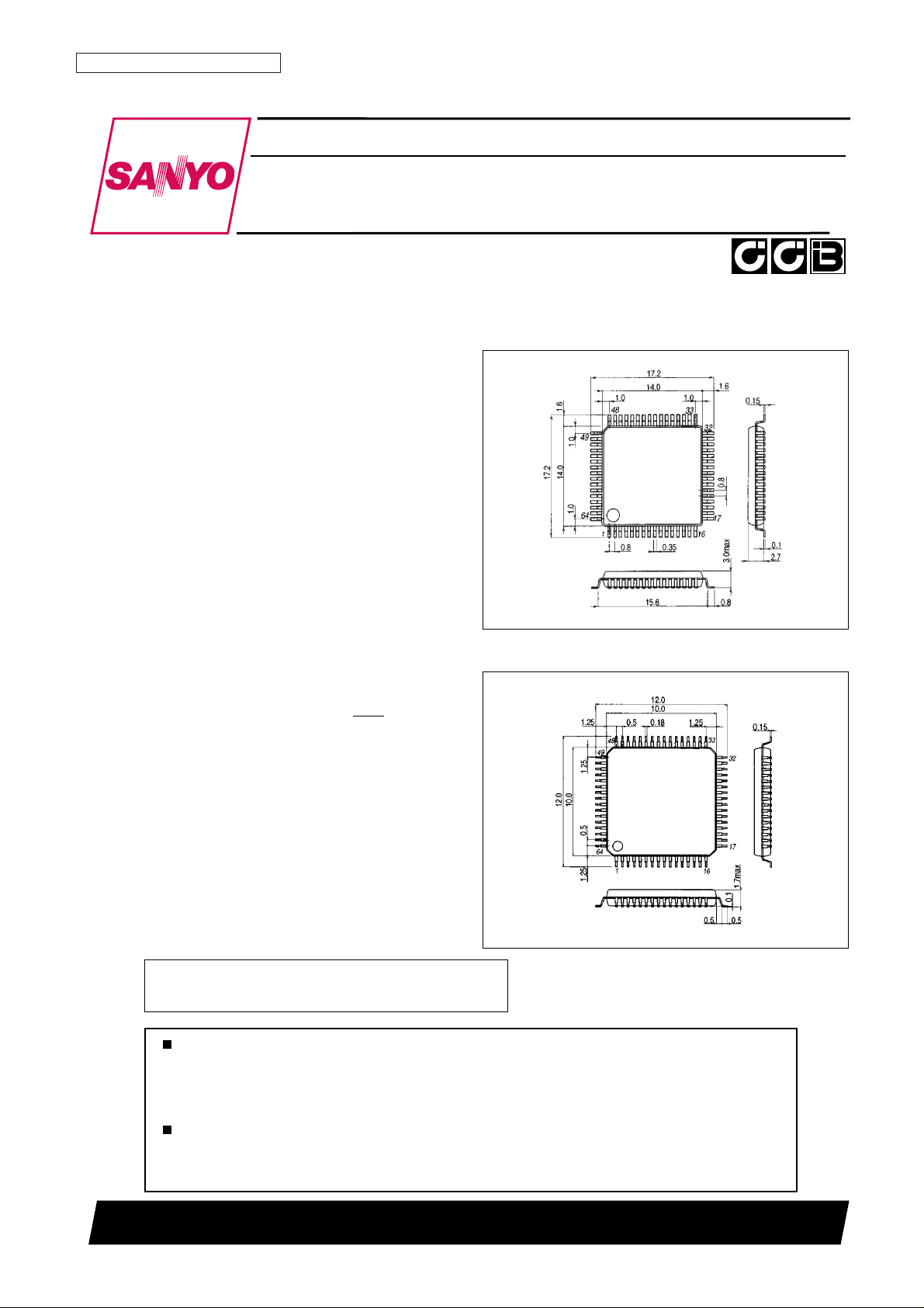
Package Dimensions
unit: mm
3151-QFP64E
unit: mm
3190-SQFP64
SANYO: QFP64E (QIP64E)
[LC75757E]
LC75757E, 75757W
SANYO Electric Co.,Ltd. Semiconductor Bussiness Headquarters
TOKYO OFFICE Tokyo Bldg., 1-10, 1 Chome, Ueno, Taito-ku, TOKYO, 110-8534 JAPAN
1/3 Duty VFD Driver with Key Input Function
CMOS IC
Any and all SANYO products described or contained herein do not have specifications that can handle
applications that require extremely high levels of reliability, such as life-support systems, aircraft’s
control systems, or other applications whose failure can be reasonably expected to result in serious
physical and/or material damage. Consult with your SANYO representative nearest you before using
any SANYO products described or contained herein in such applications.
SANYO assumes no responsibility for equipment failures that result from using products at values that
exceed, even momentarily, rated values (such as maximum ratings, operating condition ranges, or other
parameters) listed in products specifications of any and all SANYO products described or contained
herein.
• CCB is a trademark of SANYO ELECTRIC CO., LTD.
• CCB is SANYO’s original bus format and all the bus
addresses are controlled by SANYO.
SANYO: SQFP64
[LC75757W]
Page 2
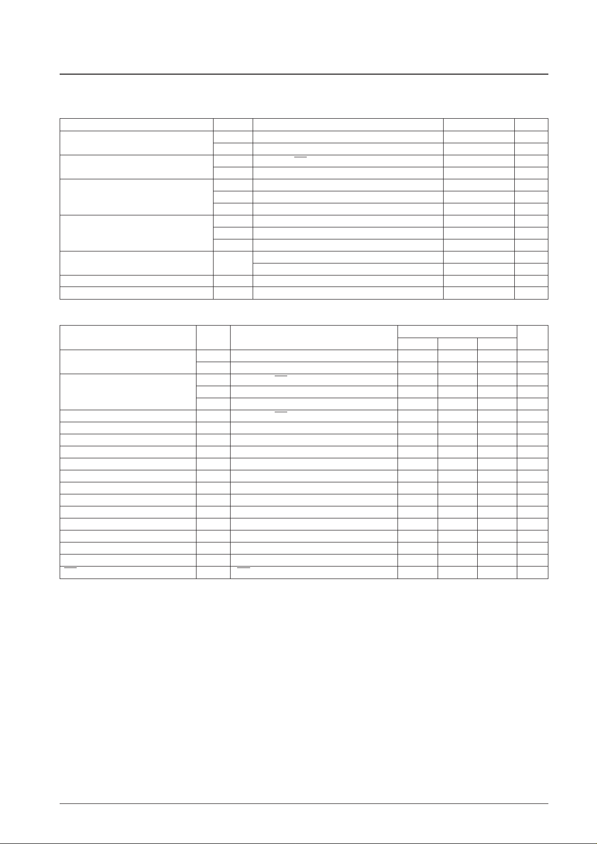
Specifications
Absolute Maximum Ratings at Ta = 25°C, VSS= 0 V
Allowable Operating Ranges at Ta = –40 to +85°C, VDD= 4.5 to 5.5 V, VSS= 0 V
Note: Since DO is an open-drain output, these values will vary with the pull-up resistance R
PU
and the load capacitance CL.
No. 5951-2/18
LC75757E, LC75757W
Parameter Symbol Conditions
Ratings
Unit
min typ max
Supply voltage
V
DD
V
DD
4.5 5.0 5.5 V
V
FL
V
FL
8 12 18 V
V
IH
1 DI, CL, CE, BLK 0.8 V
DD
5.5 V
High-level input voltage V
IH
2 OSCI 0.8 V
DD
V
DD
V
V
IH
3 KI1 to KI5 0.6 V
DD
V
DD
V
Low-level input voltage V
IL
DI, CL, CE, BLK, OSCI, KI1 to KI5 0 0.2 V
DD
V
Guaranteed oscillator frequency range f
OSC
OSCI, OSCO 0.9 2.4 3.7 MHz
Recommended external resistor value R
OSC
OSCI, OSCO 2.2 12 47 kΩ
Recommended external capacitor value C
OSC
OSCI, OSCO 15 33 100 pF
Clock low-level pulse width t
øL
CL : See figure 1. 160 ns
Clock high-level pulse width t
øH
CL : See figure 1. 160 ns
Data setup time t
ds
DI, CL : See figure 1. 160 ns
Data hold time t
dh
DI, CL : See figure 1. 160 ns
CE wait time t
cp
CE, CL : See figure 1. 160 ns
CE setup time t
cs
CE, CL : See figure 1. 160 ns
CE hold time t
ch
CE, CL : See figure 1. 160 ns
DO output delay time t
dc
DO: RPU= 4.7 kΩ, CL= 10 pF*: See figure 1. 1.5
µs
DO rise time t
dr
DO: RPU= 4.7 kΩ, CL= 10 pF*: See figure 1. 1.5
µs
BLK switching time t
c
BLK, CE : See figure 4. 10
µs
Parameter Symbol Conditions Ratings Unit
Maximum Supply voltage
V
DD
max V
DD
–0.3 to +6.5 V
V
FL
max V
FL
–0.3 to +21.0 V
Input voltage
V
IN
1 DI, CL, CE, BLK –0.3 to +6.5 V
V
IN
2 OSCI, KI1 to KI5 –0.3 to VDD+0.3 V
V
OUT
1 S1 to S41, G1 to G3 –0.3 to VFL+0.3 V
Output voltage V
OUT
2 OSCO, KS1 to KS5 –0.3 to VDD+0.3 V
V
OUT
3 DO –0.3 to +6.5 V
I
OUT
1 S1 to S41 6 mA
Output current I
OUT
2 G1 to G3 60 mA
I
OUT
3 KS1 to KS5 1 mA
Allowable power dissipation Pd max
Ta = 85°C (LC75757E) 400 mW
Ta = 85°C (LC75757W) 300 mW
Operating temperature Topr –40 to +85 °C
Storage temperature Tstg –50 to +150 °C
Page 3
• When stopped with CL at the low level
No. 5951-3/18
LC75757E, LC75757W
• When stopped with CL at the high level
Figure 1
Parameter Symbol Conditions
Ratings
Unit
min typ max
High-level input current
I
IH
1 DI, CL, CE, BLK: VIN= 5.5 V 5 µA
I
IH
2 OSCI: VIN= V
DD
5 µA
Low-level input current I
IL
DI, CL, CE, BLK, OSCI: VIN= 0 V –5 µA
Input floating voltage V
IF
KI1 to KI5 0.05 V
DD
V
Pull-down resistance R
PD
KI1 to KI5: VDD= 5.0 V 50 100 250 kΩ
Output off leakage current I
OFFH
DO: VO= 5.5 V 5 µA
V
OH
1 S1 to S41: IO= –2 mA VFL– 0.6 V
High-level output voltage
V
OH
2 G1 to G3: IO= –50 mA VFL– 1.3 V
V
OH
3 OSCO: IO= –0.5 mA VDD– 2.0 V
V
OH
4 KS1 to KS5: IO= –500 µA VDD– 1.2 VDD– 0.5 VDD– 0.2 V
V
OL
1 S1 to S41, G1 to G3: IO= 50 µA 0.5 V
Low-level output voltage
V
OL
2 OSCO: IO= 0.5 mA 2.0 V
V
OL
3 KS1 to KS5: IO= 25 µA 0.2 0.5 1.5 V
V
OL
4 DO: IO= 1 mA 0.1 0.5 V
Oscillator frequency f
OSC
R
OSC
= 12 kΩ, C
OSC
= 33 pF 2.4 MHz
Hysteresis voltage V
H
DI, CL, CE, BLK, KI1 to KI5 0.1 V
DD
V
Current drain
I
DD
1 Sleep mode 5 µA
I
DD
2 Outputs open: f
OSC
= 2.4 MHz 10 mA
Electrical Characteristics in the Allowable Operating Ranges
Page 4
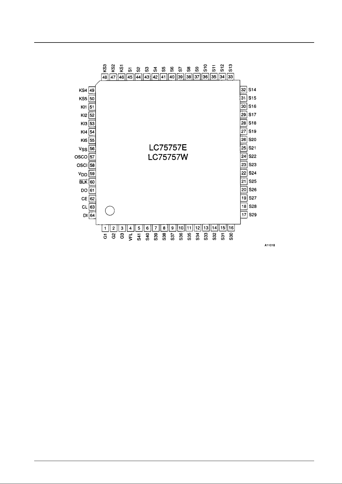
Pin Assignment
No. 5951-4/18
LC75757E, LC75757W
Top view
Page 5
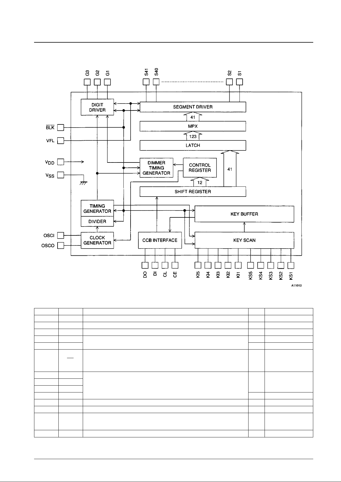
Block Diagram
Pin Descriptions
No. 5951-5/18
LC75757E, LC75757W
Pin No. Pin Function I/O Handling when unused
4 V
FL
Driver block power supply. Applications must provide a voltage in the range 8.0 to 18.0 V. — —
59 V
DD
Logic block power supply. Applications must provide a voltage in the range 4.5 to 5.5 V. — —
56 V
SS
Power supply ground. This pin must be connected to the system ground. — —
58 OSCI I GND
57 OSCO O OPEN
Reset signal input used to initialize the IC internal state. During a reset,
60 BLK
the display is turned off forcibly regardless of the internal display data.
I GND
Also note that the internal key data is all reset to 0 and key scan operations are disabled.
However, serial data input is possible in this state.
63 CL
64 DI I GND
62 CE
61 DO O OPEN
1 to 3 G1 to G3 Digit outputs. The frame frequency f
O
is (f
OSC
/6144) Hz. O OPEN
45 to 5 S1 to S41 Segment outputs that display the display data transferred over the serial interface. O OPEN
Key scan outputs. Normally, when a key matrix is formed, diodes are inserted in the key
46 to 50 KS1 to KS5 scan timing lines to prevent shorts. However, since this IC uses unbalanced CMOS outputs O OPEN
in the output transistor circuit, the IC will not be damaged if these outputs are shorted.
51 to 55 KI1 to KI5 Key scan inputs. Pull-down resistors are built into the IC internal pin circuits. I GND
Serial data interface. These pins must be connected to the system microcontroller.
Note that since DO is an open-drain output, a pull-up resistor is required.
CL: Synchronization clock DI: Transfer data
CE: Chip enable DO: Output data
Oscillator circuit connections. An oscillator circuit is formed by connecting a resistor and a
capacitor externally to these pins.
Page 6
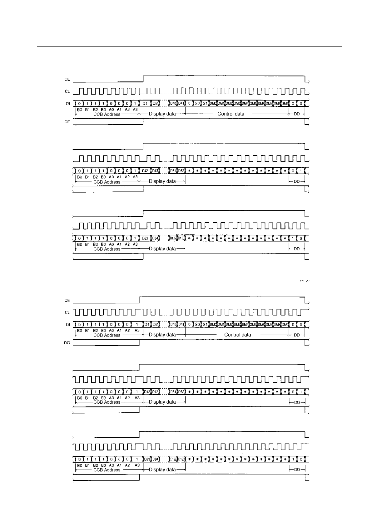
Serial Data Input
• When stopped with CL at the low level
No. 5951-6/18
LC75757E, LC75757W
Note: don’t care
DD: Direction data
• When stopped with CL at the high level
Note: don’t care
DD: Direction data
Figure 2
Page 7

• CCB address: Applications must send the value 01110001B(8EH) as shown in figure 2.
• D1 to D41: Segment display data for the G1 digit output pin
Dn (n = 1 to 41) = 1: Segment on
Dn (n = 1 to 41) = 0: Segment off
• D42 to D82: Segment display data for the G2 digit output pin
Dn (n = 42 to 82) = 1: Segment on
Dn (n = 42 to 82) = 0: Segment off
• D83 to D123: Segment display data for the G3 digit output pin
Dn (n = 83 to 123) = 1: Segment on
Dn (n = 83 to 123) = 0: Segment off
• S0, S1: Sleep control data
• DM0 to DM9: Dimmer data
Control Data
• S0, S1: Sleep control data
This control data controls switching between sleep mode and normal mode, and also sets the states of the KS1 to KS5
key scan output pins in key scan standby mode.
• DM0 to DM9: Dimmer data
This data controls the duty of the G1 to G3 digit output pins. This data forms a 10-bit binary value in which D0 is the
LSB. The brightness of the display can be controlled by adjusting the duty of the G1 to G3 digit output pins. The table
lists the relationship between the dimmer data and the dimmer value.
t3 and t4: See figure 5.
Relationship between the Display Data (D1 to D123) and the Segment Output Pins
No. 5951-7/18
LC75757E, LC75757W
Control data
Mode
Clock generator Segment outputs
Output pin states during key scan standby
S0 S1
(oscillator circuit) Digit output
KS1 KS2 KS3 KS4 KS5
0 0 Normal Oscillator operating Operating H H H H H
0 1 Sleep Stopped L L L L L H
1 0 Sleep Stopped L L L L H H
1 1 Sleep Stopped L H H H H H
DM9 DM8 DM7 DM6 DM5 DM4 DM3 DM2 DM1 DM0 Dimmer value (t4/t3)
0 0 0 0 0 0 0 0 0 0 0/1024
0 0 0 0 0 0 0 0 0 1 1/1024
0 0 0 0 0 0 0 0 1 0 2/1024
to to
1 1 1 1 1 1 1 1 0 0 1020/1024
1 1 1 1 1 1 1 1 0 1 1021/1024
1 1 1 1 1 1 1 1 1 0 1022/1024
1 1 1 1 1 1 1 1 1 1 Illegal setting
Segment
G1 G2 G3
output pin
S1 D1 D42 D83
S2 D2 D43 D84
S3 D3 D44 D85
S4 D4 D45 D86
S5 D5 D46 D87
S6 D6 D47 D88
S7 D7 D48 D89
S8 D8 D49 D90
S9 D9 D50 D91
S10 D10 D51 D92
S11 D11 D52 D93
S12 D12 D53 D94
S13 D13 D54 D95
S14 D14 D55 D96
Segment
G1 G2 G3
output pin
S15 D15 D56 D97
S16 D16 D57 D98
S17 D17 D58 D99
S18 D18 D59 D100
S19 D19 D60 D101
S20 D20 D61 D102
S21 D21 D62 D103
S22 D22 D63 D104
S23 D23 D64 D105
S24 D24 D65 D106
S25 D25 D66 D107
S26 D26 D67 D108
S27 D27 D68 D109
S28 D28 D69 D110
Segment
G1 G2 G3
output pin
S29 D29 D70 D111
S30 D30 D71 D112
S31 D31 D72 D113
S32 D32 D73 D114
S33 D33 D74 D115
S34 D34 D75 D116
S35 D35 D76 D117
S36 D36 D77 D118
S37 D37 D78 D119
S38 D38 D79 D120
S39 D39 D80 D121
S40 D40 D81 D122
S41 D41 D82 D123
Page 8

As an example, the table below lists the operation of the S11 segment output pin.
Serial Data Output
• When stopped with CL at the low level
• When stopped with CL at the high level
• CCB address: Applications must send the value 11110001B(8FH) as shown in figure 3.
• KD1 to KD25: Key data
• SA: Sleep acknowledge data
Note: The key data (KD1 to KD25) and the sleep acknowledge data (SA) will be invalid if the key data is read when DO
is high.
No. 5951-8/18
LC75757E, LC75757W
Display data
Segment output pin (S11) state
D11 D52 D93
0 0 0 The segments corresponding to the G1 to G3 digit output pins are off
0 0 1 The segment corresponding to the G3 digit output pin is turned on
0 1 0 The segment corresponding to the G2 digit output pin is on
0 1 1 The segments corresponding to the G2 and G3 digit output pins are on
1 0 0 The segment corresponding to the G1 digit output pin is on
1 0 1 The segments corresponding to the G1 and G3 digit output pins are on
1 1 0 The segments corresponding to the G1 and G2 digit output pins are on
1 1 1 The segments corresponding to the G1 to G3 digit output pins are on
Figure 3
CCB address
CCB address
Page 9

Output Data
• KD1 to KD25: Key data
These bits represent the key output states when a key matrix with up to 25 keys is formed using the KS1 to KS5 key
scan output pins and the KI1 to KI5 key scan input pins. When a key is pressed, the bit corresponding to that key will
be set to 1. The correspondence is listed in the following table.
• SA: Sleep acknowledge data
This output data is set to the state when the key was pressed. In that case DO will go to the low level. If serial data is
input during this period and the mode is set (normal mode or sleep mode), the IC will be set to that mode. SA is set to
1 in the sleep mode and to 0 in the normal mode.
Sleep Mode
The IC is set to sleep mode by setting either S0 or S1 in the control data to 1. The segment outputs and the digit outputs
are all set low, and the clock generator (oscillator circuit) is stopped (although it is restarted when a key is pressed), and
thus power dissipation is reduced. This mode is cleared by setting S0 and S1 in the control data to 0.
Key Scan Operation
• Key scan timing
The scan period is 18000T [s]. A key scan is performed twice to reliably recognize the key on/off states by verifying
that the key data for the two scans agrees. If the data agrees, the IC recognizes a key press and 38400T [s] after the
start of key scan execution issues a key scan data read request by outputting a low level from DO. If the key data does
not agree and a key was pressed at the later scan, the IC executes another key scan operation. Note that this means that
this IC cannot recognize a key press shorter than 38400T [s].
Note *: The high-level and low-level states in sleep mode are set according to the control data S0 and S1. Key scan output signals are not output from pins
set to the “L” state.
No. 5951-9/18
LC75757E, LC75757W
Item KI1 KI2 KI3 KI4 KI5
KS1 KD1 KD2 KD3 KD4 KD5
KS2 KD6 KD7 KD8 KD9 KD10
KS3 KD11 KD12 KD13 KD14 KD15
KS4 KD16 KD17 KD18 KD19 KD20
KS5 KD21 KD22 KD23 KD24 KD25
Page 10

• In normal mode
— The pins KS1 to KS5 are set high.
—
A key scan is started when any of the keys is pressed, and the keys are kept scanning until all keys are released.
The controller can recognize simultaneous multiple key presses by checking the key data for multiple bits being set.
— If a key is pressed for over 38400T [s] (where T = 1/f
OSC
), the IC outputs a key data read request to the controller
by setting DO low. The controller acknowledges this state and reads the key data. However, note that DO will go
high when CE is set high during the serial data transfer.
— After the controller key data readout completes, the key data read request will be cleared (DO will be set high), and
the IC performs another key scan. Note that since DO is an open-drain output, a pull-up resistor (between 1 and
10 kΩ) is required.
• In sleep mode
— The pins KS1 to KS5 are set to high or low according to the values of S0 and S1 in the control data. (See the
description of the control data elsewhere in this document.)
—
If a key connected to one of the KS1 to KS5 lines that was set high is pressed, the clock generator (oscillator circuit)
is started and a key scan is performed, and the keys are kept scanning until all keys are released.
The controller can recognize simultaneous multiple key presses by checking the key data for multiple bits being set.
— If a key is pressed for over 38400T [s] (where T = 1/f
OSC
), the IC outputs a key data read request to the controller
by setting DO low. The controller acknowledges this state and reads the key data. However, note that DO will go
high when CE is set high during the serial data transfer.
— After the controller key data readout completes, the key data read request will be cleared (DO will be set high), and
the IC performs another key scan. However, sleep mode will not be cleared. Note that since DO is an open-drain
output, a pull-up resistor (between 1 and 10 kΩ) is required.
— Example of a key scan operation in sleep mode
Example: Sleep mode with S1 = 0, S1 = 1 (Only KS5 is set high)
Note *: These diodes are required to reliably recognize multiple key presses on the KS5 line when the IC is set to sleep mode with only KS5 set to high as in
the example above. That is, they prevent incorrect recognition of key presses due to sneak currents arising from simultaneous presses of keys on
the KS1 through KS4 lines.
No. 5951-10/18
LC75757E, LC75757W
If one of these keys is pressed, clock
generator (oscillator circuit) is started and
a key scan is performed.
Serial data transfer
Key input 1
Key input 2
Key scan
Serial data transfer
Serial data transfer
Key data read
Key data read request
Key data read
Key data read request
Key data read
Key data read request
Key address (8FH)
Key address
Key address
Page 11

Multiple Key Presses
The LC75757E/W, even without diodes in the key scan lines, can scan for any combination of dual key presses, any
combination of triple key presses on any of the KI1 to KI5 key scan input pin lines, or any combination of multiple key
presses on any of the KS1 to KS5 key scan output lines. However, keys that are not pressed may be seen as having been
pressed for any other multiple key press combination. Accordingly, applications must insert diodes at each key. Also, to
reject any triple and higher multiple key presses, if three or more data readout are 1 ignore the data by the software or in
other ways.
Notes on the BLK Pin and Display Control
Since the states of the IC internal data (D1 to D123, and the control data) are undefined when power is first applied,
applications should turn off the display (i.e. set S1 to S41, and G1 to G3 low) by setting the BLK pin low at the same
time as power is applied. Applications should transfer all 192 bits of the serial data while BLK is held low, and only then
set BLK high. This will prevent random meaningless display at power on. (See figure 4.)
Note on the Power on Sequence
Applications must observe the following sequences when turning the power on or off.
• At power on: First turn on the logic system power (VDD), and then turn on the driver power (VFL)
• At power off: First turn off the driver power (VFL), and then turn off the logic system power (VDD).
No. 5951-11/18
LC75757E, LC75757W
Serial data transfer
Serial data transfer
Serial data transfer
Key data read
Key data read request
Key data read
Key data read request
Key address (8FH) Key address
Figure 4
Display and control data transfer
Undefined Defined Undefined
Undefined Defined Undefined
Undefined Defined Undefined
Key input
(KS5 line)
Key scan
Internal data
D1 to D41
Control data
Internal data
D42 to D82
Internal data
D83 to D123
Page 12

Output Waveforms (S1 to S41)
No. 5951-12/18
LC75757E, LC75757W
G1
G2
G3
S1 to S41 waveform when the segment
corresponding to G1 is on.
S1 to S41 waveform when the segment
corresponding to G2 is on.
S1 to S41 waveform when the segment
corresponding to G3 is on.
S1 to S41 waveform when the segments
corresponding to G1 and G2 are on.
S1 to S41 waveform when the segments
corresponding to G1 and G3 are on.
S1 to S41 waveform when the segments
corresponding to G2 and G3 are on.
S1 to S41 waveform when the segments
corresponding to G1, G2, and G3 are on.
S1 to S41 waveform when the segments
corresponding to G1, G2, and G3 are off.
Page 13

Relationship between the Segment and Digit Outputs
• Figure 5 shows the case where the display data is set up so that the segment outputs S1 to S41 output the VSSlevel
with the same timing as the G1 and G3 digit outputs, and output the VFLlevel with the same timing as the G2 digit
output. Here, the segments corresponding to G2 will be turned on. The relationship between t3 and the oscillator
frequency f
OSC
in this case is t3 = 2048/f
OSC
.
• The G1 to G3 digit output waveforms in example 1 correspond to a dimmer data (DM0 to DM9) set to 3FEH. The
relationship between t1 and the oscillator frequency f
OSC
is t1 = 2/f
OSC
. Note that t1 and t2 in example 1 are identical
times.
• The G1 to G3 digit output waveforms in example 2 correspond to a dimmer data (DM0 to DM9) set to a smaller value.
Although t1 does not change, t2 becomes longer. Here, if the dimmer data (DM0 to DM9) is set to 1FFHand the
oscillator frequency f
OSC
is 2.4 MHz, then t2 can be calculated as follows.
• If the dimmer data (DM0 to DM9) is set to an even smaller value, t2 will become even longer as shown in example 3.
Note that t1 does not change in this case as well.
No. 5951-13/18
LC75757E, LC75757W
Example 1
S1 to S41
Example 2
Example 3
t2 = t3 – t1 × (1FFH+1)
=
1024
f
OSC
= 0.43 [ms]
Figure 5
Page 14

Block States during the Reset Period (when BLK is low)
• Divider and timing generator
These circuits are reset and their base clock is stopped.
• Dimmer timing generator
The circuit is reset and its operation is stopped.
• Digit and segment drivers
These circuits are reset and the display is turned off (S1 to S41 and G1 to G3 are set low.)
• Key scan
The circuit is reset, its internal circuits are set to the initial state, and key scanning is disabled.
• Key buffer
The circuit is reset and all data is set to 0.
• Clock generator
The state (normal or sleep mode) of this block (the clock oscillator circuit) is determined after the sleep control data
(S0 and S1) is transferred.
• CCB interface, shift register, control register, latch, and multiplexer
These circuits are not reset so that serial data can be input during the reset period.
No. 5951-14/18
LC75757E, LC75757W
: Blocks that are reset.
Page 15

Output Pin States during the Reset Period (when BLK is low)
Notes: 1. The state of this pin is undefined after power has been applied until the sleep control data (S0 and S1) are transferred.
2. Since this pin is an open-drain output, a pull-up resistor (between 1 and 10 kΩ) is required. It remains high during the reset period even if the
controller attempts to read the key data.
Sample Application Circuit
Note *: Since DO is an open-drain output, a pull-up resistor is required. Select a value in the range 1 to 10 kΩ that is most appropriate for the capacitance
of the external lines so that the waveform is not distorted.
Notes on the Segment and Digit Waveforms
The segment waveform is somewhat deformed due to the VFD panel itself and the circuit wiring. Furthermore, if a digit
waveform such as digit waveform 1 in which no dimming is applied is used, the display will glow dimly. Therefore,
applications must take this waveform deformation into account and apply adequate dimming such as that shown in digit
waveform 2 so that this phenomenon does not occur.
No. 5951-15/18
LC75757E, LC75757W
Output pin State during reset
S1 to S4 L
G1 to G3 L
KS1 to KS4 X *
1
KS5 H
DO H *
2
From the controller
Key matrix with
up to 25 keys
To the controller
To the controlle
power supply
VFD panel with up to 123 segments
Segment waveform
Digit waveform 1
Digit waveform 2
Figure 6
Page 16

Notes on Controller Transfer of Display Data
Since the display data is transferred in three operations as shown in figure 2, we strongly recommend that applications
transfer all the data within a 30 ms period to assure display quality.
Controller Key Data Readout Procedure
When the controller uses a timer to read out the key data
• Flowchart
• Timing chart
t5
.........
Key scan execution time (38400T [s]) when the key data for two key scan operations matches.
t6
........
Key scan execution time (76800T [s]) when the key data for the first two key scan operations
............does not match.
t7
.........
Key address (8FH) transfer time
t8
.........
Key data readout time
• Operation
When the controller use timer processing for key on/off determination and key data readout, it must set CE low and
check the state of DO at least once every t9 period. If DO is low, the controller must recognize that a key has been
pressed and read out the key data.
The period t9 must obey the following inequality:
t9 > t7 + t8 + t6
Note that if the controller reads out key data when DO is high, both the key data (KD1 to KD25) and the sleep
acknowledge data will be invalid data.
No. 5951-16/18
LC75757E, LC75757W
T =
1
[s]
f
OSC
Controller
determination
(Key on)
Controller
determination
(Key on)
Controller
determination
(Key off)
Controller
determination
(Key on)
Controller
determination
(Key off)
Page 17

When the controller uses interrupt processing to read out the key data
• Flowchart
• Timing chart
t5.........Key scan execution time (38400T [s]) when the key data for two key scan operations matches.
t6 ........Key scan execution time (76800T [s]) when the key data for the first two key scan operations
............does not match.
t7......... Key address (8FH) transfer time
t8.........Key data readout time
• Operation
When the controller uses interrupt processing for key on/off determination and key data readout, it must check the state
of DO when CE is low, and perform a key data readout if DO is low. The next time the controller checks the on/off
states of the keys, it must make that determination at a time t10 after the last readout based on the state of DO when
CE is low, and then read out the key data. The time t10 must obey the following inequality:
t10 > t6
Note that if the controller reads out key data when DO is high, both the key data (KD1 to KD25) and the sleep
acknowledge data will be invalid data.
No. 5951-17/18
LC75757E, LC75757W
T =
1
[s]
f
OSC
Wait period
(at least t10)
Controller
determination
(Key on)
Controller
determination
(Key off)
Controller
determination
(Key on)
Controller
determination
(Key on)
Controller
determination
(Key on)
Controller
determination
(Key off)
Page 18

PS No. 5951-18/18
LC75757E, LC75757W
This catalog provides information as of November, 1998. Specifications and information herein are
subject to change without notice.
Specifications of any and all SANYO products described or contained herein stipulate the performance,
characteristics, and functions of the described products in the independent state, and are not guarantees
of the performance, characteristics, and functions of the described products as mounted in the customer’s
products or equipment. To verify symptoms and states that cannot be evaluated in an independent device,
the customer should always evaluate and test devices mounted in the customer’s products or equipment.
SANYO Electric Co., Ltd. strives to supply high-quality high-reliability products. However, any and all
semiconductor products fail with some probability. It is possible that these probabilistic failures could
give rise to accidents or events that could endanger human lives, that could give rise to smoke or fire,
or that could cause damage to other property. When designing equipment, adopt safety measures so
that these kinds of accidents or events cannot occur. Such measures include but are not limited to protective
circuits and error prevention circuits for safe design, redundant design, and structural design.
In the event that any or all SANYO products (including technical data, services) described or contained
herein are controlled under any of applicable local export control laws and regulations, such products must
not be exported without obtaining the export license from the authorities concerned in accordance with the
above law.
No part of this publication may be reproduced or transmitted in any form or by any means, electronic or
mechanical, including photocopying and recording, or any information storage or retrieval system,
or otherwise, without the prior written permission of SANYO Electric Co., Ltd.
Any and all information described or contained herein are subject to change without notice due to
product/technology improvement, etc. When designing equipment, refer to the “Delivery Specification”
for the SANYO product that you intend to use.
Information (including circuit diagrams and circuit parameters) herein is for example only; it is not
guaranteed for volume production. SANYO believes information herein is accurate and reliable, but
no guarantees are made or implied regarding its use or any infringements of intellectual property rights
or other rights of third parties.
 Loading...