

Page 1
Ordering number : EN5950
101698RM (OT) No. 5950-1/10
LC75754M
SANYO Electric Co.,Ltd. Semiconductor Bussiness Headquarters
TOKYO OFFICE Tokyo Bldg., 1-10, 1 Chome, Ueno, Taito-ku, TOKYO, 110-8534 JAPAN
1/3 Duty VFD Driver
CMOS IC
Any and all SANYO products described or contained herein do not have specifications that can handle
applications that require extremely high levels of reliability, such as life-support systems, aircraft’s
control systems, or other applications whose failure can be reasonably expected to result in serious
physical and/or material damage. Consult with your SANYO representative nearest you before using
any SANYO products described or contained herein in such applications.
SANYO assumes no responsibility for equipment failures that result from using products at values that
exceed, even momentarily, rated values (such as maximum ratings, operating condition ranges, or other
parameters) listed in products specifications of any and all SANYO products described or contained
herein.
Overview
The LC75754M is a 1/3 duty VFD driver that can be used
for electronic tuning frequency display and other
applications under the control of a microcontroller. This
product can directly drive VFDs with up to 72 segments.
Features
• 72 segment outputs.
• Noise reduction circuits are built into the output drivers.
• Serial data input supports CCB format communication
with the system controller.
• Dimmer can be controlled by serial data input.
• High generality since display data is displayed without
the intervention of a decoder.
• All segments can be turned off with the BLK pin.
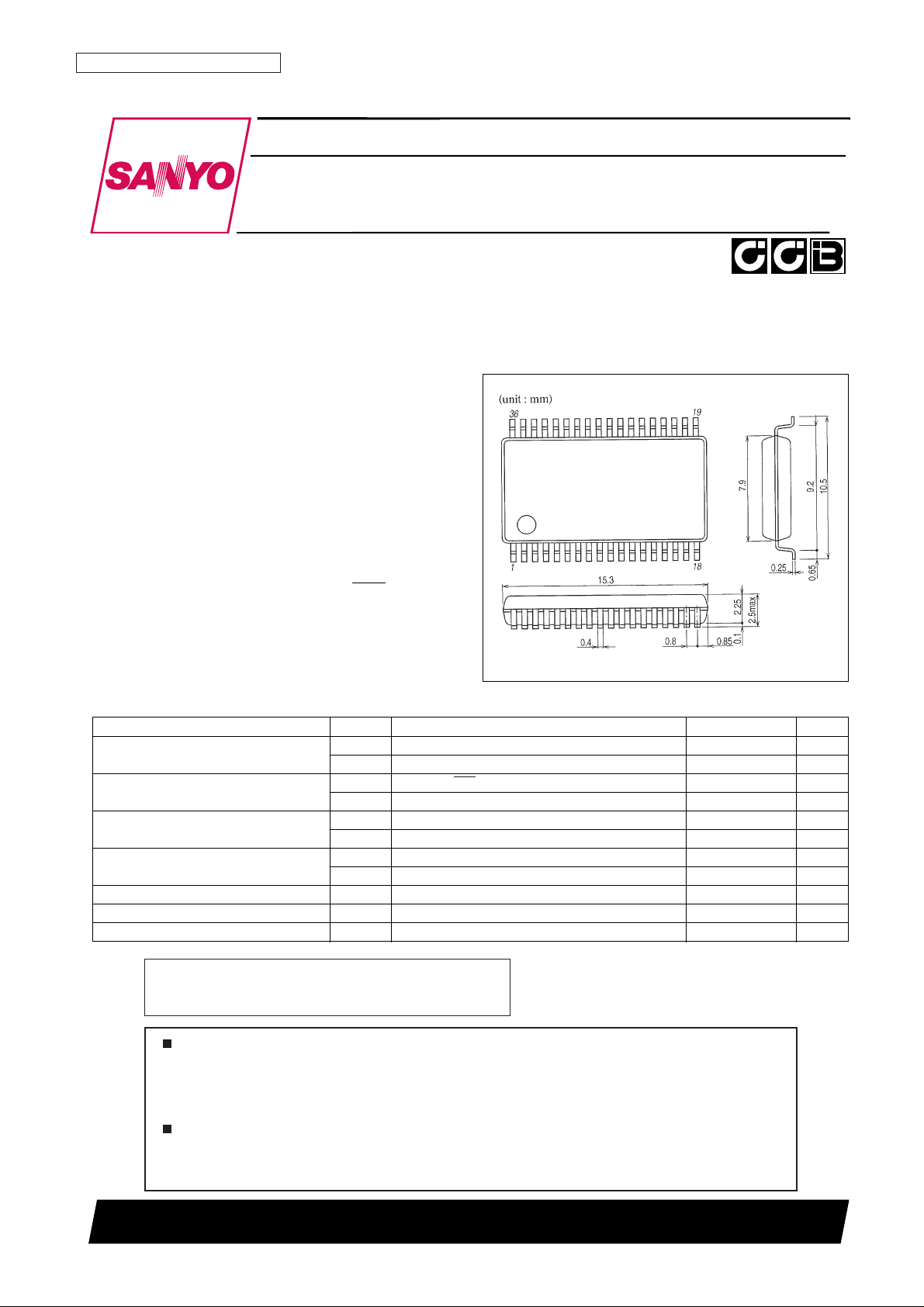
Package Dimensions
unit: mm
3129-MFP36S
SANYO: MFP36S
[LC75754M]
Parameter Symbol Conditions Ratings Unit
Maximum supply voltage
V
DD
max V
DD
–0.3 to +6.5 V
V
FL
max V
FL
–0.3 to +21.0 V
Input voltage
V
IN
1 DI, CL, CE, BLK –0.3 to +6.5 V
V
IN
2 OSCI –0.3 to VDD+0.3 V
Output voltage
V
OUT
1 S1 to S24, G1 to G3 –0.3 to VFL+0.3 V
V
OUT
2 OSCO –0.3 to VDD+0.3 V
Output current
I
OUT
1 S1 to S24 6 mA
I
OUT
2 G1 to G3 60 mA
Allowable power dissipation Pd max Ta = 85°C 300 mW
Operating temperature Topr –40 to +85 °C
Storage temperature Tstg –50 to +150 °C
Specifications
Absolute Maximum Ratings at Ta = 25°C, VSS= 0V
• CCB is a trademark of SANYO ELECTRIC CO., LTD.
• CCB is SANYO’s original bus format and all the bus
addresses are controlled by SANYO.
Page 2
No. 5950-2/10
LC75754M
Allowable Operating Ranges at Ta = –40 to +85°C, VDD= 4.5 to 5.5V, VSS= 0V
Parameter Symbol Conditions
Ratings
Unit
min typ max
Supply voltage
V
DDVDD
4.5 5.0 5.5 V
V
FL
V
FL
8 12 18 V
Input high-level voltage
V
IH
1 DI, CL, CE, BLK 0.8 V
DD
5.5 V
V
IH
2 OSCI 0.8 V
DD
V
DD
V
Input low-level voltage V
IL
DI, CL, CE, BLK, OSCI 0 0.2 V
DD
V
Guaranteed oscillator range f
OSC
OSCI, OSCO 0.9 2.4 3.7 MHz
Recommended external resistance R
OSC
OSCI, OSCO 2.2 12 47 KΩ
Recommended external capacitance C
OSC
OSCI, OSCO 15 33 100 pF
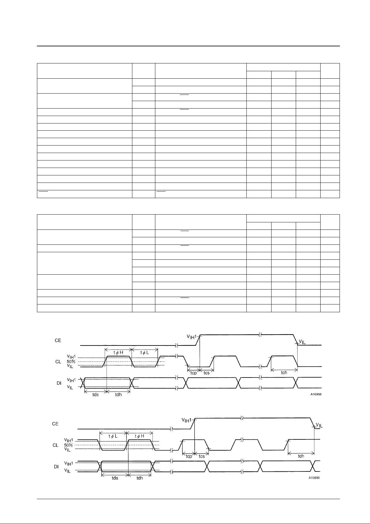
Low level clock pulse width t
øL
CL : Figure 1 160 ns
High level clock pulse width t
øH
CL : Figure 1 160 ns
Data setup time t
ds
DI, CL : Figure 1 160 ns
Data hold time t
dh
DI, CL : Figure 1 160 ns
CE wait time t
cp
CE, CL : Figure 1 160 ns
CE setup time t
cs
CE, CL : Figure 1 160 ns
CE hold time t
ch
CE, CL : Figure 1 160 ns
BLK switching time t
c
BLK, CE : Figure 3 10 µs
Electrical Characteristics in the Allowable Operating Ranges
• When CL is stopped at the low level
Parameter Symbol Conditions
Ratings
Unit
min typ max
Input high-level current
I
IH
1 DI, CL, CE, BLK : VIN= 5.5V 5 µA
I
IH
2 OSCI : VIN= V
DD
5 µA
Input low-level current I
IL
DI, CL, CE, BLK, OSCI : VIN= 0 V –5 µA
V
OH
1 S1 to S24 : IO= –2 mA VFL– 0.6 V
Output high-level voltage V
OH
2 G1 to G3 : IO= –50 mA VFL– 1.3 V
V
OH
3 OSCO : IO= –0.5 mA VDD– 2.0 V
Output low-level voltage
V
OL
1 S1 to S24, G1 to G3 : IO= 50 µA 0.5 V
V
OL
2 OSCO : IO= 0.5 mA 2.0 V
Oscillator frequency f
OSCROSC
= 12kΩ, C
OSC
= 33 pF 2.4 MHz
Hysteresis voltage V
H
DI, CL, CE, BLK 0.1 V
DD
V
Current drain I
DD
Output open : f
OSC
= 2.4MHz 10 mA
• When CL is stopped at the high level
Figure 1
Page 3
No. 5950-3/10
LC75754M
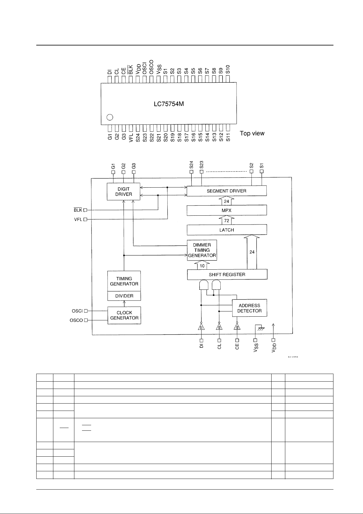
Pin Assignment
Block Diagram
Pin Functions
Pin No. Pin Function I/O Handling when unused
4 V
FL
Driver block power supply. A voltage of between 8.0 and 18.0 V must be supplied. — —
32 V
DD
Logic block power supply. A voltage of between 4.5 and 5.5 V must be supplied. — —
29 V
SS
Power supply. Must be connected to the system ground. — —
31 OSCI Oscillator connection. An oscillator circuit is formed by connecting an external resistor and I GND
30 OSCO capacitor to these pins. O OPEN
Display off control input.
33 BLK
BLK = L (V
SS
) ...........Display off (S1 to S24, G1 to G3 = L)
I GND
BLK = H (V
DD
) ..........Display on
Note that serial data can be transferred while the display is turned off.
35 CL
Serial data transfer inputs. These pins must be connected to the system microcontroller.
36 DI
CL : Synchronization clock DI : Transfer data CE : Chip enable
I GND
34 CE
1 to 3 G1 to G3 Digit outputs. The frame frequency fo is (f
OSC
/6144)Hz. O OPEN
28 to 5 S1 to S24 Segment outputs for displaying the display data transferred by serial data input O OPEN
Page 4
No. 5950-4/10
LC75754M
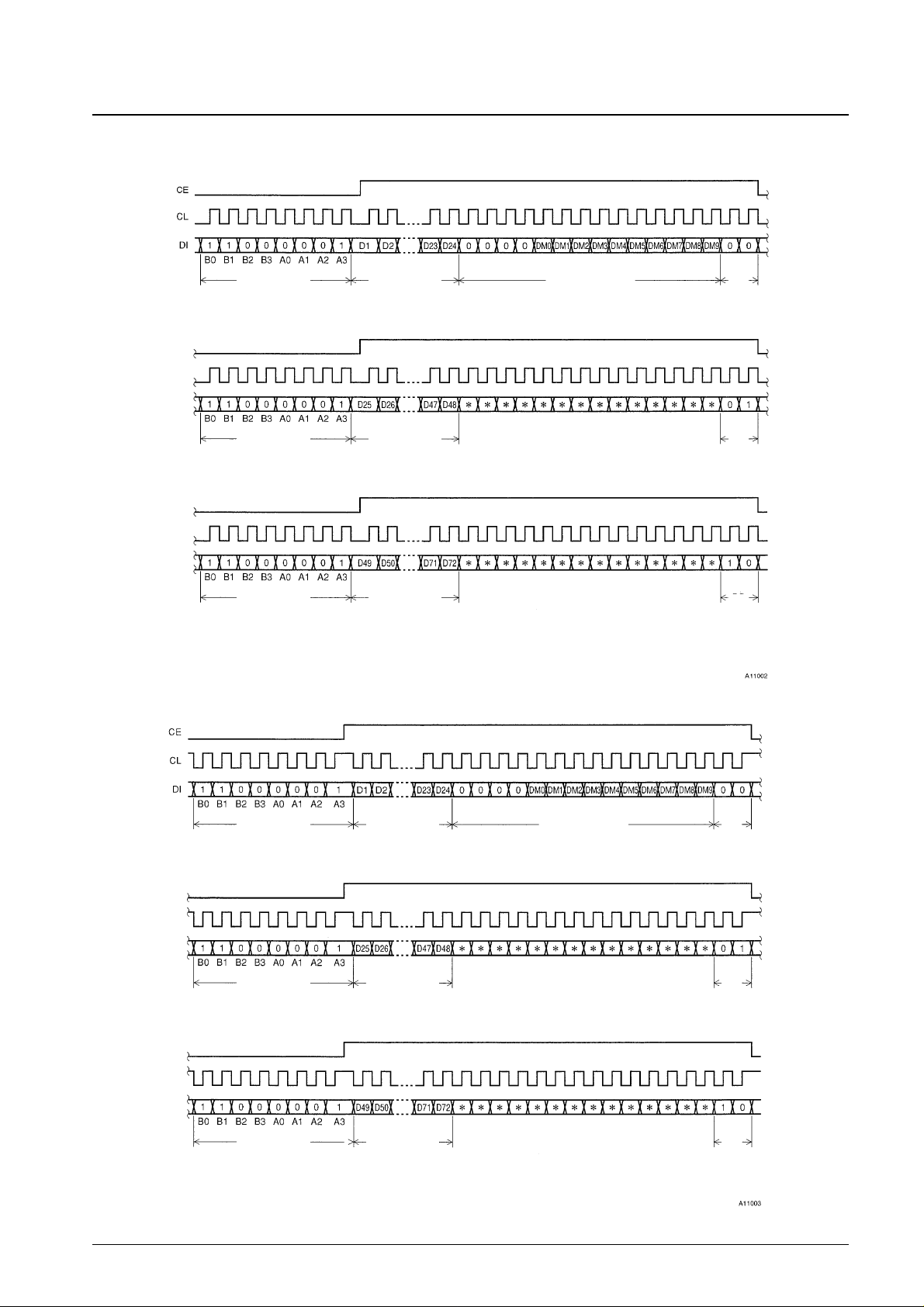
Serial Data Transfer Format
• When CL is stopped at the low level
• When CL is stopped at the high level
Figure 2
* : don’t care
DD: direction data
* : don’t care
DD: direction data
CCB address
8 bits
Display data
24 bits
Control data
14 bits
DD
2 bits
CCB address
8 bits
Display data
24 bits
Control data
14 bits
DD
2 bits
CCB address
8 bits
Display data
24 bits
DD
2 bits
CCB address
8 bits
Display data
24 bits
DD
2 bits
CCB address
8 bits
Display data
24 bits
DD
2 bits
CCB address
8 bits
Display data
24 bits
DD
2 bits
Page 5

No. 5950-5/10
LC75754M
CCB address : Transfer 11000001B(83H) as shown in Figure 2
DM0 to DM9 : Dimmer data
This data controls the duty of the G1 to G3 digit output pins, and consists of 10 bits with DM0 being
the LSB. Note that the intensity of the display can be adjusted by controlling the duty of the G1 to G3
digit output pins.
The relationship between the dimmer data and the dimmer value is as follows.
D1 to D24 : Display data for the G1 digit output pin.
Dn (n = 1 to 24) = 1 : On
Dn (n = 1 to 24) = 0 : Off
D25 to D48 : Display data for the G2 digit output pin.
Dn (n = 25 to 48) = 1 : On
Dn (n = 25 to 48) = 0 : Off
D49 to D72 : Display data for the G3 digit output pin.
Dn (n = 49 to 72) = 1 : On
Dn (n = 49 to 72) = 0 : Off
t3, t4 : See Figure 4.
DM9 DM8 DM7 DM6 DM5 DM4 DM3 DM2 DM1 DM0 Dimmer value (t4/t3)
0 0 0 0 0 0 0 0 0 0 0/1024
0 0 0 0 0 0 0 0 0 1 1/1024
0 0 0 0 0 0 0 0 1 0 2/1024
1 1 1 1 1 1 1 1 0 0 1020/1024
1 1 1 1 1 1 1 1 0 1 1021/1024
1 1 1 1 1 1 1 1 1 0 1022/1024
1 1 1 1 1 1 1 1 1 1 Not used
Correspondence between Display Data (D1 to D72) and Segment Output Pins
Example : Segment output pin S11 is controlled as follows :
Segment output pins G1 G2 G3
S1 D1 D25 D49
S2 D2 D26 D50
S3 D3 D27 D51
S4 D4 D28 D52
S5 D5 D29 D53
S6 D6 D30 D54
S7 D7 D31 D55
S8 D8 D32 D56
S9 D9 D33 D57
S10 D10 D34 D58
S11 D11 D35 D59
S12 D12 D36 D60
Segment output pins G1 G2 G3
S13 D13 D37 D61
S14 D14 D38 D62
S15 D15 D39 D63
S16 D16 D40 D64
S17 D17 D41 D65
S18 D18 D42 D66
S19 D19 D43 D67
S20 D20 D44 D68
S21 D21 D45 D69
S22 D22 D46 D70
S23 D23 D47 D71
S24 D24 D48 D72
Display data
Segment output pin S11 state
D11 D35 D59
0 0 0 The segments corresponding to the G1, G2, and G3 digit output pins are off
0 0 1 The segments corresponding to the G3 digit output pin are on
0 1 0 The segments corresponding to the G2 digit output pin are on
0 1 1 The segments corresponding to the G2 and G3 digit output pins are on
1 0 0 The segments corresponding to the G1 digit output pin are on
1 0 1 The segments corresponding to the G1 and G3 digit output pins are on
1 1 0 The segments corresponding to the G1 and G2 digit output pins are on
1 1 1 The segments corresponding to the G1, G2, and G3 digit output pins are on
Page 6

No. 5950-6/10
LC75754M
BLK and the Display Control
Since the IC internal data (D1 to D72 and the control data) is undefined when power is first applied, the display is off (S1
to S24, G1 to G3 = low) by setting the BLK pin low at the same time as power is applied. Then, meaningless display at
power on can be prevented by transferring all 144 bits of serial data from the controller and setting BLK pin high after
the transfer completes while the display is off. (See figure 3.)
Power Supply Sequence
The following sequences must be observed when power is turned on and off. (See Figure 3.)
• Power on : Logic block power supply (VDD) on → Driver block power supply (VFL) on
• Power off : Driver block power supply (VFL) off → Logic block power supply (VDD) off
Figure 3
ton > 0
toff1 > 0
toff2 > 0 (toff1 > toff2)
tc...10 µs min
Internal data
(D1 to D24, control data)
Internal data
(D25 to D48)
Internal data
(D40 to D72)
Transfer of display and control data
Undefined UndefinedDefined
Undefined UndefinedDefined
Undefined UndefinedDefined
V
DD
VFL
BLK
CE
Page 7

No. 5950-7/10
LC75754M
Output Waveforms (S1 to S24)
S1 to S24 output waveforms on G1 side being lighted
S1 to S24 output waveforms on G2 side being lighted
S1 to S24 output waveforms on G3 side being lighted
S1 to S24 output waveform on G1 and G2 sides being lighted
S1 to S24 output waveform on G1 and G3 sides being lighted
S1 to S24 output waveform on G2 and G3 sides being lighted
S1 to S24 output waveform on G1 to G3 sides being lighted
S1 to S24 output waveform on G1 to G3 sides being unlighted
G1
G2
G3
Page 8

No. 5950-8/10
LC75754M
Relationship between Segment and Digit outputs
Figure 4
Example 1
S1 to S24
Example 2
Example 3
• Consider the examples shown in Figure 4, where display data is set up so that the segment outputs S1 to S24 output
VSSlevel on the G1 and G3 digit output timing and VFLlevel on the G2 digit output timing. (Here, the G2 side being
lighted) The relationship between the time t3 and the oscillator frequency f
OSC
is t3 = 2048/f
OSC
.
• The digit output G1 to G3 waveforms in Example 1 are output when the dimmer data (DM0 to DM9) are set to
3FEH. The relationship between the time t1 and the oscillator frequency f
OSC
is t1=2/f
OSC
. Note that the time t1 and
the time t2 are the same period in Example 1.
• The digit output G1 to G3 waveforms in Example 2 are those when the dimmer data (DM0 to DM9) are set to a
smaller value. Although the time t1 does not change, the time t2 becomes longer.
When the dimmer data (DM0 to DM9) are set to 1FFHand the oscillator frequency fosc is 2.4 [MHz], then the time
t2 is :
t2 = t3 – t1 × (1FFH+ 1)
1024
= ——
f
OSC
= 0.43[ms]
• When the dimmer data (DM0 to DM9) are set to an even smaller value, the time t2 becomes even longer, as in
example 3. Note that the time t1 does not change here, either.
Page 9

No. 5950-9/10
LC75754M
Sample Application Circuit
Notes on the Segment and Digit Waveforms
The segment waveform is distorted by the VFD panel used and the wiring, and furthermore, in the case of being used
with essentially no dimming as in the digit waveform 1, as shown in Figure 5, the VFD panel glow dimly. By carefully
considering the segment waveform, it can be seen that this problem can be resolved by applying an adequate amount of
dimming, as shown in digit waveform 2.
Notes on Transferring Display Data from the Controller
Since display data is transferred in three operations as shown in Figure 2, we recommend that all display data be
transferred within 30 [ms] to prevent degradation of the visual quality of the displayed image.
VFD panel (up to 72 segments)
From the controller
Segment waveform
Digit waveform 1
Digit waveform 2
Figure 5
Page 10

PS No. 5950-10/10
LC75754M
This catalog provides information as of October, 1998. Specifications and information herein are subject
to change without notice.
Specifications of any and all SANYO products described or contained herein stipulate the performance,
characteristics, and functions of the described products in the independent state, and are not guarantees
of the performance, characteristics, and functions of the described products as mounted in the customer’s
products or equipment. To verify symptoms and states that cannot be evaluated in an independent device,
the customer should always evaluate and test devices mounted in the customer’s products or equipment.
SANYO Electric Co., Ltd. strives to supply high-quality high-reliability products. However, any and all
semiconductor products fail with some probability. It is possible that these probabilistic failures could
give rise to accidents or events that could endanger human lives, that could give rise to smoke or fire,
or that could cause damage to other property. When designing equipment, adopt safety measures so
that these kinds of accidents or events cannot occur. Such measures include but are not limited to protective
circuits and error prevention circuits for safe design, redundant design, and structural design.
In the event that any or all SANYO products (including technical data, services) described or contained
herein are controlled under any of applicable local export control laws and regulations, such products must
not be exported without obtaining the export license from the authorities concerned in accordance with the
above law.
No part of this publication may be reproduced or transmitted in any form or by any means, electronic or
mechanical, including photocopying and recording, or any information storage or retrieval system,
or otherwise, without the prior written permission of SANYO Electric Co., Ltd.
Any and all information described or contained herein are subject to change without notice due to
product/technology improvement, etc. When designing equipment, refer to the “Delivery Specification”
for the SANYO product that you intend to use.
Information (including circuit diagrams and circuit parameters) herein is for example only; it is not
guaranteed for volume production. SANYO believes information herein is accurate and reliable, but
no guarantees are made or implied regarding its use or any infringements of intellectual property rights
or other rights of third parties.
 Loading...