

Page 1
Ordering number : EN*4907
31595TH (OT) No. 4907-1/21
Overview
The LC75710NE series products are dot matrix VFD
controller/driver LSIs that display characters, numbers,
and symbols. These LSIs generate dot matrix VFD drive
signals based on serial data sent from a microprocessor,
and allow display systems to be implemented easily using
the built-in character generator ROM and RAM.
The LC75710NE series products are fabricated in a
CMOS process and can contribute to achieving low-power
operation in user applications.
Features
•5 × 7 dot matrix VFD display controller/driver
(Driver outputs can be connected directly to VFD
devices: pull-down resistors are not required.)
• Display technique: Dynamic lighting technique
• Display digits: 1 to 16 digits (programmable)
• Display control data
CGROM: 5 × 7 dots, 160 characters
CGRAM: 5 × 7 dots, 8 characters
ADRAM: 16 × 8 bits
DCRAM: 64 × 8 bits
• Instruction functions
Display on/off control
Display shift
Display blink
Intensity adjustment (dimmer)
• Serial data input (DI, CL, and CE pins)
• Built-in reset circuit
• 64-pin flat package
Differences between the LC75710NE,
LC75711NE, and LC75712E
• The data in the built-in character generator ROM
(CGROM) differs between these products. All other
functions are identical.
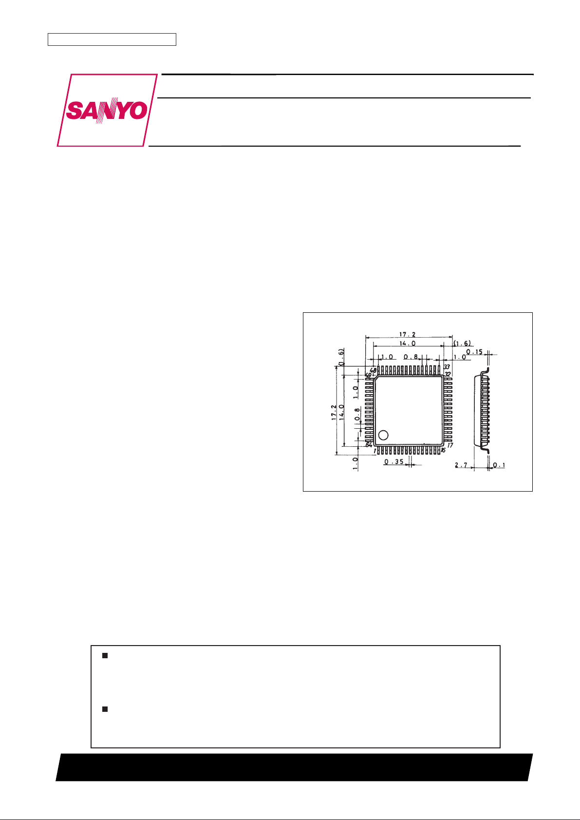
Package Dimensions
unit: mm
3159-QFP64E
Preliminary
SANYO: QIP64E
[LC75710NE, 75711NE, 75712E]
LC75710NE, 75711NE, 75712E
SANYO Electric Co.,Ltd. Semiconductor Bussiness Headquarters
TOKYO OFFICE Tokyo Bldg., 1-10, 1 Chome, Ueno, Taito-ku, TOKYO, 110-8534 JAPAN
Dot Matrix VFD Display Controller/Driver
CMOS LSI
Any and all SANYO products described or contained herein do not have specifications that can handle
applications that require extremely high levels of reliability, such as life-support systems, aircraft’s
control systems, or other applications whose failure can be reasonably expected to result in serious
physical and/or material damage. Consult with your SANYO representative nearest you before using
any SANYO products described or contained herein in such applications.
SANYO assumes no responsibility for equipment failures that result from using products at values that
exceed, even momentarily, rated values (such as maximum ratings, operating condition ranges, or other
parameters) listed in products specifications of any and all SANYO products described or contained
herein.
Page 2
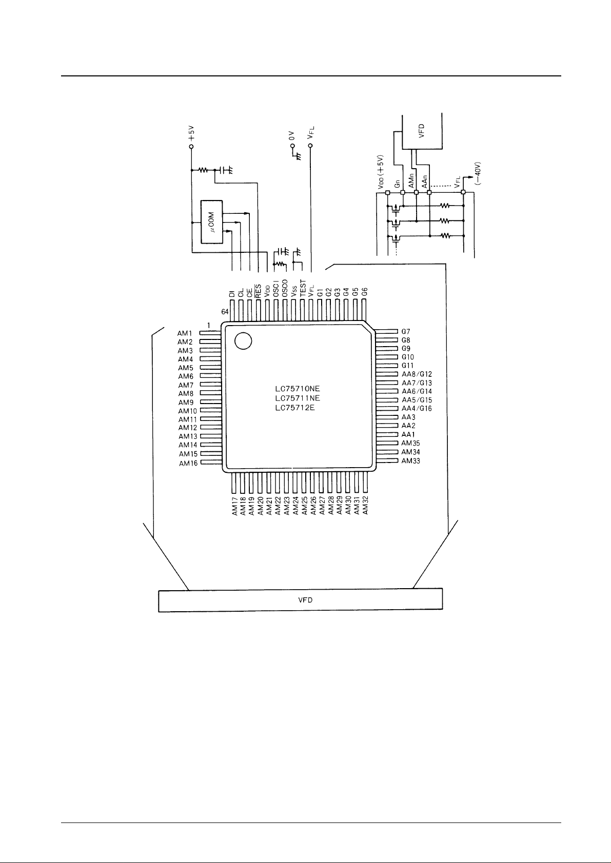
Pin Assignment and Sample Application Circuit
No. 4907-2/21
LC75710NE, 75711NE, 75712E
Page 3
Specifications
Absolute Maximum Ratings at Ta = 25°C, VSS= 0 V
Allowable Operating Ranges at Ta = –40 to +85°C, VDD= 4.5 to 5.5 V, VSS= 0 V
No. 4907-3/21
LC75710NE, 75711NE, 75712E
Parameter Symbol Conditions Ratings Unit
Maximum supply voltage
V
DD
max V
DD
–0.3 to +6.5
V
V
FL
max V
FL
VDD– 55 to VDD+ 0.3
Input voltage
V
IN
1 OSCI –0.3 to VDD+ 0.3
V
V
IN
2 DI, CL, CE, RES –0.3 to +6.5
I
OUT
1 AM1 to AM35 1
Output current I
OUT
2 AA1 to AA3 10 mA
I
OUT
3 AA4 to AA8, G1 to G16 20
Allowable power dissipation Pd max
Ta ≤ 85°C, with up to 70% of the AM1 to AM35
400 mW
outputs driven
Operating temperature Topr –40 to +85 °C
Storage temperature Tstg –50 to +125 °C
Parameter Symbol Conditions min typ max Unit
Supply voltage
V
DD
V
DD
4.5 5.0 5.5
V
V
FL
V
FL
VDD– 50 V
DD
VIH1 DI, CL, CE 0.8 V
DD
5.5
Input high level voltage V
IH
2 RES 0.7 V
DD
5.5 V
V
IH
3 OSCI 0.7 V
DD
V
DD
Input low level voltage
V
IL
1 DI, CL, CE 0 0.2 V
DD
V
V
IL
2 RES, OSCI 0 0.3 V
DD
Guaranteed oscillator range f
OSC
OSCI, OSCO 1.0 2.7 3.5 MHz
Recommended external resistor R
OSC
OSCI, OSCO 10 kΩ
Recommended external capacitor C
OSC
OSCI, OSCO 30 pF
Minimum reset pulse width t
WRES
RES 1 µs
Low level clock pulse width t
øL
CL 0.5 µs
High level clock pulse width t
øH
CL 0.5 µs
Data setup time t
DS
DI, CL 0.5 µs
Data hold time t
DH
DI, CL 0.5 µs
CE wait time t
CP
CE, CL 0.5 µs
CE setup time t
CS
CE, CL 0.5 µs
CE hold time t
CH
CE, CL 0.5 µs
Page 4
Electrical Characteristics within the Allowable Operating Ranges
Note: Since this IC incorporates high voltage ports it is easily damaged by static discharges. Therefore, extra care is required when handling this IC.
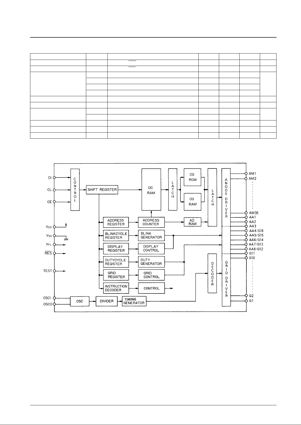
Block Diagram
No. 4907-4/21
LC75710NE, 75711NE, 75712E
Parameter Symbol Conditions min typ max Unit
Input high level current I
IH
DI, CL, CE, RES, OSCI: Vi = 5.5 V 5 µA
Input low level current I
IL
DI, CL, CE, RES, OSCI: Vi = 0 V –5 µA
V
OH
1 AM1 to AM35: IO= 1 mA VDD– 1.0
Output high level voltage
V
OH
2 AA1 to AA3: IO= 10 mA VDD– 1.0
V
V
OH
3 AA4 to AA8, G1 to G16: IO= 20 mA VDD– 2.0
V
OH
4 OSCO: IO= 0.5 mA VDD– 2.0 V
DD
Output low level voltage V
OL
OSCO: IO= –0.5 mA 0 2.0 V
Output off voltage V
OFF
AM1 to AM35, AA1 to AA8, G1 to G16: VFL= VDD– 50 V VDD– 49 V
Pull-down resistors
R
1
AM1 to AM35: VDD– VFL= 48 V 140 650
kΩ
R
2
AA1 to AA8, G1 to G16: VDD– VFL= 48 V 70 325
Oscillator frequency f
OSC
R = 10 kΩ, C = 30 pF 2.16 2.7 3.24 MHz
Hysteresis voltage V
H
DI, CL, CE 0.5 V
Supply current I
DD
Outputs open, f
OSC
= 2.7 MHz, VFL= VDD– 50 V 5 mA
Page 5
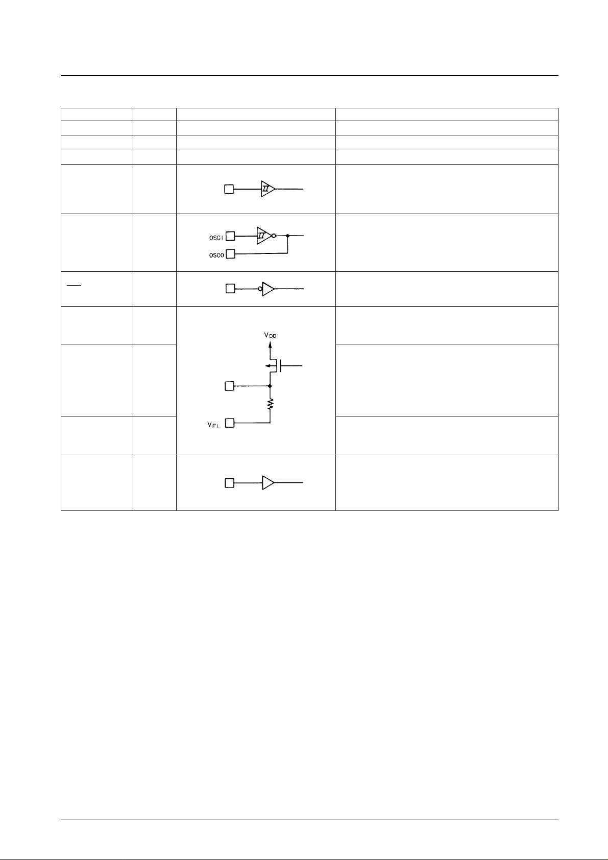
Pin Functions
No. 4907-5/21
LC75710NE, 75711NE, 75712E
Pin No. Pin circuit Function
V
DD
V
SS
V
FL
DI
CL
CE
OSCI
OSCO
RES
AM1 to AM35
AA1 to AA3
AA4/G16
AA5/G15
AA6/G14
AA7/G13
AA8/G12
G1 to G11
TEST
1
1
1
1
1
1
1
1
1
38
5
11
1
Logic block power supply: +5 V (typical)
Logic block power supply: ground
Driver block power supply
Serial data interface
DI: Transfer data
CL: Synchronization clock
CE: Chip enable
External oscillator RC circuit connections
System reset input
Anode outputs
Pull-down resistors are built in.
Anode/grid outputs
These pins function as grid output pins when the number of
displayed digits is selected to be between 12 and 16 digits with
the “Grid register load” instruction.
Pull-down resistors are built in.
Grid outputs
Pull-down resistors are built in.
LSI testing
This pin must be connected to V
SS
during normal operation.
Page 6
Block Functions
1. AC (address counter)
AC is a counter that provides addresses for DCRAM and ADRAM.
The address is modified automatically by internal operations to maintain the VFD display state.
2. DCRAM (data control RAM)
DCRAM is RAM that holds the display data, which is expressed as 8-bit character codes. (These character codes are
converted to 5 × 7 dot matrix patterns using the CGROM and CGRAM memories.) DCRAM has a capacity of 64 × 8
bits, and can hold the data for 64 characters. The relationship between the 6-bit DCRAM address in AC and the
display position on the VFD display is described below.
• When the DCRAM address in AC is 00H. (16 digits displayed)
However, the DCRAM address moves as follows when a display shift is performed by specifying MDATA.
Note: The 6-bit DCRAM addresses are expressed in hexadecimal.
3. ADRAM (additional data RAM)
ADRAM is RAM used to store ADATA display data. ADRAM has a 16 × 8-bit capacity and the stored display data
is output directly without using CGROM and CGRAM. The relationship between the 4-bit ADRAM address in AC
and the display position on the VFD display is described below.
• When the ACRAM address in AC is 0H. (16 digits displayed)
However, the ADRAM address moves as follows when a display shift is performed by specifying ADATA.
Note: DCRAM and ADRAM addresses are expressed in hexadecimal.
Example: When the DCRAM address is 3E
H
.
No. 4907-6/21
LC75710NE, 75711NE, 75712E
Display digit 16 15 14 13 12 11 10 9 8 7 6 5 4 3 2 1
DCRAM address (hexadecimal) 0F 0E 0D 0C 0B 0A 09 08 07 06 05 04 03 02 01 00
Right shift
Display digit 16 15 14 13 12 11 10 9 8 7 6 5 4 3 2 1
DCRAM address (hexadecimal) 10 0F 0E 0D 0C 0B 0A 09 08 07 06 05 04 03 02 01
Left shift
Display digit 16 15 14 13 12 11 10 9 8 7 6 5 4 3 2 1
DCRAM address (hexadecimal) 0E 0D 0C 0B 0A 09 08 07 06 05 04 03 02 01 00 3F
Display digit 16 15 14 13 12 11 10 9 8 7 6 5 4 3 2 1
ADRAM address (hexadecimal) F E D C B A 9 8 7 6 5 4 3 2 1 0
Right shift
Display digit 16 15 14 13 12 11 10 9 8 7 6 5 4 3 2 1
ADRAM address (hexadecimal) 0 F E D C B A 9 8 7 6 5 4 3 2 1
Left shift
Display digit 16 15 14 13 12 11 10 9 8 7 6 5 4 3 2 1
ADRAM address (hexadecimal) E D C B A 9 8 7 6 5 4 3 2 1 0 F
DA5 DA4 DA3 DA2 DA1 DA0
1 1 1 1 1 0
DCRAM address
Hexadecimal Hexadecimal
ADRAM address
Hexadecimal
LSBMSB
DA0DA1DA2DA3DA4DA5
LSBMSB
RA0RA1RA2RA3
Page 7

4. CGROM (character generator ROM)
CGROM is ROM that is used to generate the 160 different 5 × 7 dot matrix character patterns. It has a capacity of
160 × 35 bits. When 8-bit character codes are written to DCRAM, the CGROM character pattern corresponding to
this 8-bit character code is displayed at the VFD display position corresponding to the DCRAM address in AC.
Tables 3 to 5 show the correspondence between the character codes and the character patterns.
5. CGRAM (character generator RAM)
CGRAM is RAM to which user programs can write arbitrary data. Up to eight 5 × 7 dot matrix character patterns can
be stored in the CGRAM. CGRAM has a capacity of 8 × 35 bits.
To display a character pattern stored in CGRAM, write one of the character codes shown at the left of tables 3 to 5 to
DCRAM. The CGRAM character pattern will be displayed at the VFD position corresponding to the DCRAM
address in AC.
Reset Function
The LC75710NE series accepts a reset when a low level is applied to the RES pin. On a reset the LC75710NE series
creates a display with all VFD lamps turned off. However, note that the values in DCRAM, ADRAM, and CGRAM, as
well as the values of the duty cycle register (intensity) and the grid register (number of digits) are undefined following a
reset. Therefore, before turning on display with a display on/off control instruction, these values must be initialized. In
particular, the following instructions must be executed when power is first applied.
• Display blink
• DCRAM data write
• ADRAM data write (if ADRAM is used)
• CGRAM data write (if CGRAM is used) Initial state settings
• Set AC address
• Grid register load
• Intensity adjustment (dimmer)
After executing the above instructions the display must be turned on by executing a “Display on/off control” instruction.
Note that incorrect display may occur if the number of displayed digits and the intensity are not set up in advance. This
can occur in cases where a display on/off control instruction is executed before the grid register load and intensity
adjustment instructions are executed. To prevent this problem, always execute the following three instructions together
as a single set.
• Grid register load
• Intensity adjustment (dimmer)
• Display on/off control
No. 4907-7/21
LC75710NE, 75711NE, 75712E
Page 8

Data Input
1. Serial control data consists of an 8-bit address and a 24-bit instruction. The address is used as a chip select function
when multiple ICs are connected to the same bus. The table shows the address for the LC75710NE series.
Note: Only one instruction, the “CGRAM data write” instruction, consists of 56 bits. See Table 1 for instruction code details.
2. DI, CL, CE signal timing
Data is acquired on the rising edge of the CL signal and latched on the falling edge of the CE signal. When the
microprocessor sends multiple instructions to the LC75710NE series, it must wait long enough for the LC75710NE
series to complete the execution of each instruction before sending the next instruction.
No. 4907-8/21
LC75710NE, 75711NE, 75712E
Address
B0 B1 B2 B3 A0 A1 A2 A3
1 1 1 0 0 1 1 0
Page 9

Table 1 Instruction Table
*: Don’t care.
Note: 1.
2. The table below shows the structure of the CGRAM data write instruction.
3. f
OSC
= 2.7 MHz
No. 4907-9/21
LC75710NE, 75711NE, 75712E
Code
Grid
Blinks the display.
M = 1: MDATA specification, A = 1: ADATA specification
*1
Grid
Turns the display on or off.
O = 1: Display on, O = 0: Display off
Shifts the display.
R/L = 1: Left shift, R/L = 0: Right shift
Sets the number of digits displayed according to the grid
number data.
DCRAM Loads a DCRAM and ADRAM address into AC
address (address counter).
Duty cycle
Adjusts the VFD intensity according to the duty cycle data.
data
DCRAM Write data Specifies the DCRAM (data control RAM) address and
address (character code) writes data.
ADATA
Specifies the ADRAM (additional data RAM) address and
writes data.
CGRAM
Write data
*2
Specifies the CGRAM (character generator RAM)
address address and writes data.
Instruction
D23 D22 D21 D20 D19 D18 D17 D16 D15 D14 D13 D12
Display blink 1 0 1 M A
Blink
cycle data
Display on/off control 0 0 0 1 * M A O
Display shift 0 0 1 0 * M A R/L * * * *
Grid register load 0 0 1 1
Grid
* * * *
number data
Set AC address 0 1 0 0
ADRAM
* *
address
Intensity adjustment (dimmer) 0 1 0 1 * * * *
DCRAM data write 0 1 1 0 * * * * * *
ADRAM data write 0 1 1 1
ADRAM
address
CGRAM data write 1 0 0 0 * * * *
Code
D47 D46 D45 D44 D43 D42 D41 D40 D39 D38 D37 D36 D35 D34 ← → D0
CGRAM address * * * * * Write data
D55 D54 D53 D52 D51 D50 D49 D48
1 0 0 0 * * * *
Description
Execution time
D11 D10 D9 D8 D7 D6 D5 D4 D3 D2 D1 D0
(maximum)
*3
18 µs
18 µs
* * * * * * * * * * * * 18 µs
* * * * * * * * * * * * 0 µs
* * * * * * * * 18 µs
* * * * * * * * 0 µs
18 µs
* * * * * * * * 18 µs
18 µs
Page 10

Detailed Instruction Descriptions
1. Display blink........................................<Blinks the display.>
M, A: Data that specifies the blinking operation
BC0 to BC2: Blink period setting
G1 to G16: Blinking digit specification
Each bit Gn (where n is an integer between 1 and 16) specifies that blinking be applied to grid output pin Gn when
the corresponding bit Gn is 1.
This instruction is used to specify the blinking operation. Not only can an arbitrary digit be specified, but MDATA
and ADATA can also be specified. There are also seven blinking periods.
Note: 1. When the blinking period needs to be controlled precisely the display should be blinked by repeatedly
turning the display on and off using the display on/off control instruction.
2. Display on/off control..........................<Turns the display on or off.>
*: Don’t care.
M, A: Specifies the data to be turned on or off.
O: On/off control
When the display is turned off with an O value of 0, the data can be displayed immediately with an O value of 1
since the display data remains in DCRAM.
No. 4907-10/21
LC75710NE, 75711NE, 75712E
Code
D15 D14 D13 D12 D11 D10 D9 D8 D7 D6 D5 D4 D3 D2 D1 D0
G16 G15 G14 G13 G12 G11 G10 G9 G8 G7 G6 G5 G4 G3 G2 G1
D23 D22 D21 D20 D19 D18 D17 D16
1 0 1 M A BC2 BC1 BC0
M A Display operating state
0 0 Neither MDATA nor ADATA blinks.
0 1 Only ADATA blinks.
1 0 Only MDATA blinks.
1 1 Both ADATA and MDATA blink.
BC2 BC1 BC0 HEX
Blink Period (s)
*1
(when f
OSC
is 2.7 MHz)
0 0 0 0 Blink operation is stopped.
0 0 1 1 0.1
0 1 0 2 0.2
0 1 1 3 0.3
1 0 0 4 0.4
1 0 1 5 0.5
1 1 0 6 0.8
1 1 1 7 1.0
Code
D15 D14 D13 D12 D11 D10 D9 D8 D7 D6 D5 D4 D3 D2 D1 D0
G16 G15 G14 G13 G12 G11 G10 G9 G8 G7 G6 G5 G4 G3 G2 G1
D23 D22 D21 D20 D19 D18 D17 D16
0 0 0 1 * M A O
M A Display operating state
0 0 Both MDATA and ADATA turn off.
0 1 Only ADATA turns on.
1 0 Only MDATA turns on.
1 1 Both ADATA and MDATA turn on.
O Display state
0 Off
1 On
Page 11

G1 to G16: Display digit specification
Each bit Gn (where n is an integer between 1 and 16) specifies that the corresponding grid output pin Gn be turned
on when that bit (Gn) is 1.
This instruction is used to specify the display on/off control operation. Not only can an arbitrary digit be specified,
but MDATA and ADATA can also be specified.
3. Display shift.........................................<Shifts the display.>
*: Don’t care.
M, A: Specifies the data to be shifted.
R/L: Shift direction specification
4. Grid register load .................................<Specifies the number of digits displayed.>
*: Don’t care.
GN0 to GN3: Displayed digits specification
The AA4/G16, AA5/G15, AA6/G14, AA7/G13, and AA8/G12 anode/grid output pins function as grid output pins if
between 12 and 16 digits are selected. Also, this instruction must be executed prior to turn the display on since the
value of the grid register is undefined immediately after power is applied.
No. 4907-11/21
LC75710NE, 75711NE, 75712E
Code
D23 D22 D21 D20 D19 D18 D17 D16
0 0 1 0 * M A R/L
D15 D14 D13 D12 D11 D10 D9 D8 D7 D6 D5 D4 D3 D2 D1 D0
* * * * * * * * * * * * * * * *
M A Shift operating state
0 0 Neither MDATA nor ADATA are shifted.
0 1 Only ADATA is shifted.
1 0 Only MDATA is shifted.
1 1 Both MDATA and ADATA are shifted.
R/L Shift direction
0 Right shift
1 Left shift
Code
D23 D22 D21 D20 D19 D18 D17 D16
0 0 1 1 GN3 GN2 GN1 GN0
D15 D14 D13 D12 D11 D10 D9 D8 D7 D6 D5 D4 D3 D2 D1 D0
* * * * * * * * * * * * * * * *
GN3 GN2 GN1 GN0 HEX Digits Controlled
0 0 0 0 0 G1 to G16
0 0 0 1 1 G1
0 0 1 0 2 G1 to G2
0 0 1 1 3 G1 to G3
0 1 0 0 4 G1 to G4
0 1 0 1 5 G1 to G5
0 1 1 0 6 G1 to G6
0 1 1 1 7 G1 to G7
1 0 0 0 8 G1 to G8
1 0 0 1 9 G1 to G9
1 0 1 0 A G1 to G10
1 0 1 1 B G1 to G11
1 1 0 0 C G1 to G12
1 1 0 1 D G1 to G13
1 1 1 0 E G1 to G14
1 1 1 1 F G1 to G15
Page 12

5. Set AC address.....................................<Specifies the DCRAM and ADRAM addresses for AC.>
*: Don’t care.
DA0 to DA5: DCRAM address
DA0....................LSB (least significant bit)
DA5....................MSB (most significant bit)
RA0 to RA3: ADRAM address
RA0....................LSB
RA3....................MSB
This instruction loads the 6-bit DA0 to DA5 DCRAM address and the 4-bit RA0 to RA3 ADRAM address into AC.
6. Intensity adjustment.............................<Adjusts the VFD intensity.>
*: Don’t care.
DC0 to DC7: Duty cycle data (intensity adjustment data)
DC0....................LSB
DC7....................MSB
The data in the 8 bits DC0 to DC7 sets the VFD intensity to one of 240 levels. Since the value in the duty cycle
register is undefined immediately after power is applied, the display intensity is not determined at that point.
Therefore, applications must execute this instruction before turning on the display. Applications can adjust the
intensity using the duty cycle register and grid register. The duty cycle register value sets the pulse width (A) and the
grid register value sets the period (B). See Figure 3 for the grid timing chart details.
No. 4907-12/21
LC75710NE, 75711NE, 75712E
Code
D23 D22 D21 D20 D19 D18 D17 D16
0 1 0 0 RA3 RA2 RA1 RA0
D15 D14 D13 D12 D11 D10 D9 D8 D7 D6 D5 D4 D3 D2 D1 D0
* * DA5 DA4 DA3 DA2 DA1 DA0 * * * * * * * *
Code
D23 D22 D21 D20 D19 D18 D17 D16
0 1 0 1 * * * *
D15 D14 D13 D12 D11 D10 D9 D8 D7 D6 D5 D4 D3 D2 D1 D0
DC7 DC6 DC5 DC4 DC3 DC2 DC1 DC0 * * * * * * * *
Page 13

7. DCRAM data write..............................<Specifies the DCRAM address and stores data at that address.>
*: Don’t care.
DA0 to DA5: DCRAM address
DA0....................LSB
DA5....................MSB
AC0 to AC7: DCRAM write data (character code)
AC0....................LSB
AC7....................MSB
This instruction writes the 8 bits of data AC0 to AC7 to DCRAM. This data is a character code (see Tables 3 to 5)
and is converted to 5 × 7 dot matrix display data using CGROM and CGRAM.
8. ADRAM data write..............................<Specifies the ADRAM address and stores data at that address.>
*: Don’t care.
RA0 to RA3: ADRAM address
RA0....................LSB
RA3....................MSB
AD1 to AD8: ADATA display data
There are 8 bits of additional display data, referred to as ADATA, in addition to the 5 × 7 dot matrix of display data
(MDATA). This data is used to generate arbitrary dot patterns without using CGROM or CGRAM. The figures show
the correspondence between these data types. In particular, when ADn = 1 (where n is an integer between 1 and 8),
the dot AAn will be turned on.
No. 4907-13/21
LC75710NE, 75711NE, 75712E
Code
D23 D22 D21 D20 D19 D18 D17 D16
0 1 1 0 * * * *
D15 D14 D13 D12 D11 D10 D9 D8 D7 D6 D5 D4 D3 D2 D1 D0
* * DA5 DA4 DA3 DA2 DA1 DA0 AC7 AC6 AC5 AC4 AC3 AC2 AC1 AC0
Code
D23 D22 D21 D20 D19 D18 D17 D16
0 1 1 1 RA3 RA2 RA1 RA0
D15 D14 D13 D12 D11 D10 D9 D8 D7 D6 D5 D4 D3 D2 D1 D0
AD8 AD7 AD6 AD5 AD4 AD3 AD2 AD1 * * * * * * * *
ADATA Corresponding output pin
AD1 AA1
AD2 AA2
AD3 AA3
AD4 AA4/G16
AD5 AA5/G15
AD6 AA6/G14
AD7 AA7/G13
AD8 AA8/G12
Page 14

9. CGRAM data write..............................<Specifies the CGRAM address and stores data at that address.>
*: Don’t care.
CA0 to CA7: CGRAM address
CA0....................LSB
CA7....................MSB
CD1 to CD35: CGRAM write data (5 × 7 dot matrix display data)
The bit CDn (where n is an integer between 1 and 35), corresponds to the AMn dot display data. The figure below
shows the positional relationship for this display data.
No. 4907-14/21
LC75710NE, 75711NE, 75712E
Code
D55 D54 D53 D52 D51 D50 D49 D48
1 0 0 0 * * * *
D47 D46 D45 D44 D43 D42 D41 D40
CA7 CA6 CA5 CA4 CA3 CA2 CA1 CA0
Code
D39 D38 D37 D36 D35 D34 D33 D32
* * * * *
CD35 CD34 CD33
D31 D30 D29 D28 D27 D26 D25 D24
CD32 CD31 CD30 CD29 CD28 CD27 CD26 CD25
Code
D23 D22 D21 D20 D19 D18 D17 D16
CD24 CD23 CD22 CD21 CD20 CD19 CD18 CD17
D15 D14 D13 D12 D11 D10 D9 D8
CD16 CD15 CD14 CD13 CD12 CD11 CD10 CD9
Code
D7 D6 D5 D4 D3 D2 D1 D0
CD8 CD7 CD6 CD5 CD4 CD3 CD2 CD1
Page 15

Usage Notes
1. Power supply sequence
The sequences shown below must be followed when turning the power supply on and off. (See Figure 1.)
Power on: Logic block power supply (VDD) on → Driver block power supply (VFL) on → Display on (by the
execution of a display on/off control instruction)
Power off: Display off (by the execution of a display on/off control instruction) → Driver block power supply (VFL)
off → Logic block power supply (VDD) off
Fig. 1 Power Supply Sequence
2. Anode output pins
The anode output pins AM1 to AM35 are used as the anode outputs that form the 5 × 7 dot matrix due to output
current considerations. We recommend using the anode output pins AA1 to AA8 for other anode output functions.
If the anode waveform is distorted and the VFD glows slightly (smearing) due to the VFD panel used or wiring
considerations, try using a lower oscillator frequency. Refer to Figure 2 when determining the oscillator frequency.
Fig. 2 Oscillator Frequency
No. 4907-15/21
LC75710NE, 75711NE, 75712E
Page 16

Fig. 3 Grid Timing Chart (16 display digits)
No. 4907-16/21
LC75710NE, 75711NE, 75712E
Page 17

Table 2 Instruction/Display Correspondence (LC75710NE)
* Don’t care.
Note: The example above assumes the use of an 8 digit 5 × 7 dot matrix VFD, and CGRAM and ADRAM are not used.
No. 4907-17/21
LC75710NE, 75711NE, 75712E
No. Instruction (hexadecimal) Display Operation
1
2
3
4
5
6
7
8
9
10
11
12
13
14
15
16
17
18
19
Power application
(Initialization with the RES pin)
DCRAM data write
6 * 0 0 2 0
DCRAM data write
6 * 0 1 4 F
DCRAM data write
6 * 0 2 5 9
DCRAM data write
6 * 0 3 4 E
DCRAM data write
6 * 0 4 4 1
DCRAM data write
6 * 0 5 5 3
DCRAM data write
6 * 0 6 2 0
DCRAM data write
6 * 0 7 2 0
DCRAM data write
6 * 3 D 4 9
DCRAM data write
6 * 3 E 5 3
DCRAM data write
6 * 3 F 4 C
Grid register load
3 8 * * * *
Intensity adjustment
5 * F F * *
Display on/off control
1 5 0 0 F F
Display shift
2 5 * * * *
Display shift
2 5 * * * *
Display shift
2 5 * * * *
Set AC address
4 * 0 0 * *
S A N Y O
S A N Y O L
S A N Y O L S
A N Y O L S I
S A N Y O
Initializes the IC.
The display will be in the off state.
Writes display data “ ” to DCRAM address 00H.
Writes display data “O” to DCRAM address 01H.
Writes display data “Y” to DCRAM address 02H.
Writes display data “N” to DCRAM address 03H.
Writes display data “A” to DCRAM address 04H.
Writes display data “S” to DCRAM address 05H.
Writes display data “ ” to DCRAM address 06H.
Writes display data “ ” to DCRAM address 07H.
Writes display data “I’ to DCRAM address 3DH.
Writes display data “S” to DCRAM address 3EH.
Writes display data “L” to DCRAM address 3FH.
Specifies that the display has 8 digits.
Sets the VFD intensity to the maximum.
Turns on the VFD for only the digits G1 to G8 in MDATA.
Shifts the display (MDATA only) to the left.
Shifts the display (MDATA only) to the left.
Shifts the display (MDATA only) to the left.
Returns the display to the original state.
Page 18

Table 3 LC75710NE CGROM (Version for use in USA and Japan)
Note: The character pattern (output data) is undefined if the character codes 00001000Bto 00011111B, 10000000Bto 10011111B, or 11100000Bto
11111111
B
are written to DCRAM.
No. 4907-18/21
LC75710NE, 75711NE, 75712E
Page 19

Table 4 LC75711NE CGROM (Version for use in Europe)
Note: The character pattern (output data) is undefined if the character codes 00001000Bto 00011111Bor 11000000Bto 11111111Bare written to DCRAM.
No. 4907-19/21
LC75710NE, 75711NE, 75712E
Page 20

Table 5 LC75712E CGROM (Version for use in Europe)
Note: 1. The character pattern (output data) is undefined if the character codes 00001000Bto 00011111Bor 11000000Bto 11111111Bare written to
DCRAM.
2. Both the LC75711NE and the LC75712E are for use in the European market. These products differ in that the LC75712E CGROM takes handling
a 5 × 8 dot matrix into consideration. In particular, this product allows the AA1 to AA5 anode output pins to be used to form a 5 ×8 dot matrix
artificially, with the combination of AM1 to AM35 and AA1 to AA5. Adopting this structure allows applications to provide improved display quality for
European characters, especially those requiring an umlaut.
No. 4907-20/21
LC75710NE, 75711NE, 75712E
Page 21

No. 4907-21/21
LC75710NE, 75711NE, 75712E
This catalog provides information as of August, 1998. Specifications and information herein are subject to
change without notice.
Specifications of any and all SANYO products described or contained herein stipulate the performance,
characteristics, and functions of the described products in the independent state, and are not guarantees
of the performance, characteristics, and functions of the described products as mounted in the customer’s
products or equipment. To verify symptoms and states that cannot be evaluated in an independent device,
the customer should always evaluate and test devices mounted in the customer’s products or equipment.
SANYO Electric Co., Ltd. strives to supply high-quality high-reliability products. However, any and all
semiconductor products fail with some probability. It is possible that these probabilistic failures could
give rise to accidents or events that could endanger human lives, that could give rise to smoke or fire,
or that could cause damage to other property. When designing equipment, adopt safety measures so
that these kinds of accidents or events cannot occur. Such measures include but are not limited to protective
circuits and error prevention circuits for safe design, redundant design, and structural design.
In the event that any and all SANYO products described or contained herein fall under strategic
products (including services) controlled under the Foreign Exchange and Foreign Trade Control Law of
Japan, such products must not be exported without obtaining export license from the Ministry of
International Trade and Industry in accordance with the above law.
No part of this publication may be reproduced or transmitted in any form or by any means, electronic or
mechanical, including photocopying and recording, or any information storage or retrieval system,
or otherwise, without the prior written permission of SANYO Electric Co., Ltd.
Any and all information described or contained herein are subject to change without notice due to
product/technology improvement, etc. When designing equipment, refer to the “Delivery Specification”
for the SANYO product that you intend to use.
Information (including circuit diagrams and circuit parameters) herein is for example only; it is not
guaranteed for volume production. SANYO believes information herein is accurate and reliable, but
no guarantees are made or implied regarding its use or any infringements of intellectual property rights
or other rights of third parties.
 Loading...