

Page 1
Ordering number : EN6108
40799RM (OT) No. 6108-1/26
Overview
The LC75397 is an electronic volume control system
providing control over volume, balance, 4-band equalizer,
bass, and input switching based on serial inputs.
Functions
• Volume control:
The chip provides 81 levels of volume attenuation: in 1dB step between 0 dB and –79 dB and –∞.
This circuit can control a total of 5 independent
channels.
• Equalizer:
The chip provides control in 2-dB steps over the range
between +10 dB and –10 dB. Three of the four bands
have peaking equalization; the remaining one, shelving
equalization.
• Selector:
The left and right channels each offer a choice of six
inputs. The L6 and R6 inputs can be turned on and off
independently. An external constant determines the
amplification for the input signal.
• Input gain:
The input signal can be amplified by 0 to +30 dB in 2dB steps.
• Bass control:
The bass can be controlled over a ±10 dB range in 2-dB
steps.
Features
• Built-in buffer amplifiers reduce the number of external
parts required.
• Silicon gate CMOS process reduces the noise of built-in
switch.
• Built-in analog ground reference voltage generator
circuit
• All functions are controlled by serial input data. This IC
supports the CCB standard.
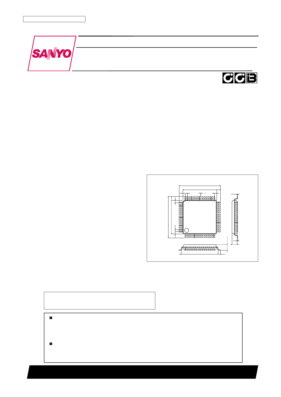
Package Dimensions
unit: mm
3159-QFP64E
14.0
17.2
1.0
1.0
1.6
0.15
0.35
0.1
15.6
0.8
0.8
3.0max
1
16
17
32
33
48
49
64
2.7
14.0
17.2
1.0
1.0
1.6
0.8
SANYO: QFP64E (QIP64E)
[LC75397]
LC75397E
SANYO Electric Co.,Ltd. Semiconductor Company
TOKYO OFFICE Tokyo Bldg., 1-10, 1 Chome, Ueno, Taito-ku, TOKYO, 110-8534 JAPAN
Single Chip Electronic Volume and Tone Control System
CMOS IC
Any and all SANYO products described or contained herein do not have specifications that can handle
applications that require extremely high levels of reliability, such as life-support systems, aircraft’s
control systems, or other applications whose failure can be reasonably expected to result in serious
physical and/or material damage. Consult with your SANYO representative nearest you before using
any SANYO products described or contained herein in such applications.
SANYO assumes no responsibility for equipment failures that result from using products at values that
exceed, even momentarily, rated values (such as maximum ratings, operating condition ranges, or other
parameters) listed in products specifications of any and all SANYO products described or contained
herein.
• CCB is a trademark of SANYO ELECTRIC CO., LTD.
• CCB is SANYO’s original bus format and all the bus
addresses are controlled by SANYO.
Page 2
No. 6108-2/26
LC75397E
Parameter Symbol Conditions Ratings Unit
Maximum supply voltage V
DD
max V
DD
11 V
Maximum input voltage V
IN
max
CL, DI, CE, L1 to L6, R1 to R6, LTIN, RTIN, LVR1IN, V
SS
– 0.3 to
V
RVR1IN, LVR2IN, RVR2IN, LVR3IN V
DD
+ 0.3
Allowable power dissipation Pd max Ta ≤ 75°C, with PC board* 1000 mW
Operating temperature Topr –30 to +75 °C
Storage temperature Tstg –40 to +125 °C
Specifications
Absolute Maximum Ratings at Ta = 25°C, VSS= 0 V
Note : * Printed circuit board size: 76.1 × 114.3 × 1.6 mm, printed circuit board material: glass/Epoxy resin
Parameter Symbol Conditions
Ratings
Unit
min typ max
Supply voltage V
DD
V
DD
6.0 10.5 V
Input high level voltage V
IH
CL, DI, CE 4.0 V
DD
V
Input low level voltage V
IL
CL, DI, CE V
SS
1.0 V
Input voltage amplitude V
IN
CL, DI, CE, L1 to L6, R1 to R6, LTIN, RTIN, LVR1IN,
V
SS
V
DD
Vp-p
RVR1IN, LVR2IN, RVR2IN, LVR3IN
Input pulse width t
øW
CL 1.0 µs
Setup time t
SETUP
CL, DI, CE 1.0 µs
Hold time t
HOLD
CL, DI, CE 1.0 µs
Operating frequency fopg CL 500 kHz
Allowable Operating Ranges at Ta = – 30 to + 75°C, VSS= 0 V
Parameter Symbol Conditions
Ratings
Unit
min typ max
[Input block]
Input resistance Rin L1 to L6, R1 to R6 50 kΩ
Clipping level Vcl LSELO, RSELO: THD = 1.0% 3.00 Vrms
Output load resistance R
L
LSELO, RSELO 10 kΩ
[Volume control block]
Input resistance Rin LVR1IN, RVR1IN, LVR2IN, RVR2IN, LVR3IN 50 kΩ
[Bass control block]
Control range Geq Max, boost/cut ±8 ±10 ±12 dB
Step resolution Estep 1 2 3 dB
Internal feedback resistance
Rbb1 1.3
kΩ
Rbb2 58
[F1/F2 band equalizer control block]
Control range Geq Max. boost/cut ±8 ±10 ±12 dB
Step resolution Estep 1 2 3 dB
Internal feedback resistor Rfeed 31 51.8 73 kΩ
[F3/F4 band equalizer control block]
Control range Geq Max. boost/cut ±8 ±10 ±12 dB
Step resolution Estep 1 2 3 dB
Internal feedback resistor Rfeed 17 28 39 kΩ
[Overall characteristics]
Total harmonic distortion THD V
IN
= 1 Vrms, f = 1 kHz, with all controls flat overall 0.01 %
Crosstalk CT
V
IN
= 1 Vrms, f = 1 kHz, with all controls flat overall,
80 dB
Rg = 1 kΩ
Output noise voltage
VN1 With all controls flat overall, 80 kHz, L.P.F 10.2 µV
V
N
2
Bass band = +10dB, With all controls overall, 80 kHz, L.P.F
10.6 µV
Output at maximum attenuation V
O
min With all controls flat overall –90 dB
Current drain I
DD
VDD– VSS= 10.5 V 58 mA
Input high level current I
IH
CL, DI, CE, VIN= 10.5 V 10 µA
Input low level current I
IL
CL, DI, CE, VIN= 0 V –10 µA
Electrical Characteristics at Ta = 25°C, VDD= 10 V, VSS= 0 V
Page 3
No. 6108-3/26
LC75397E
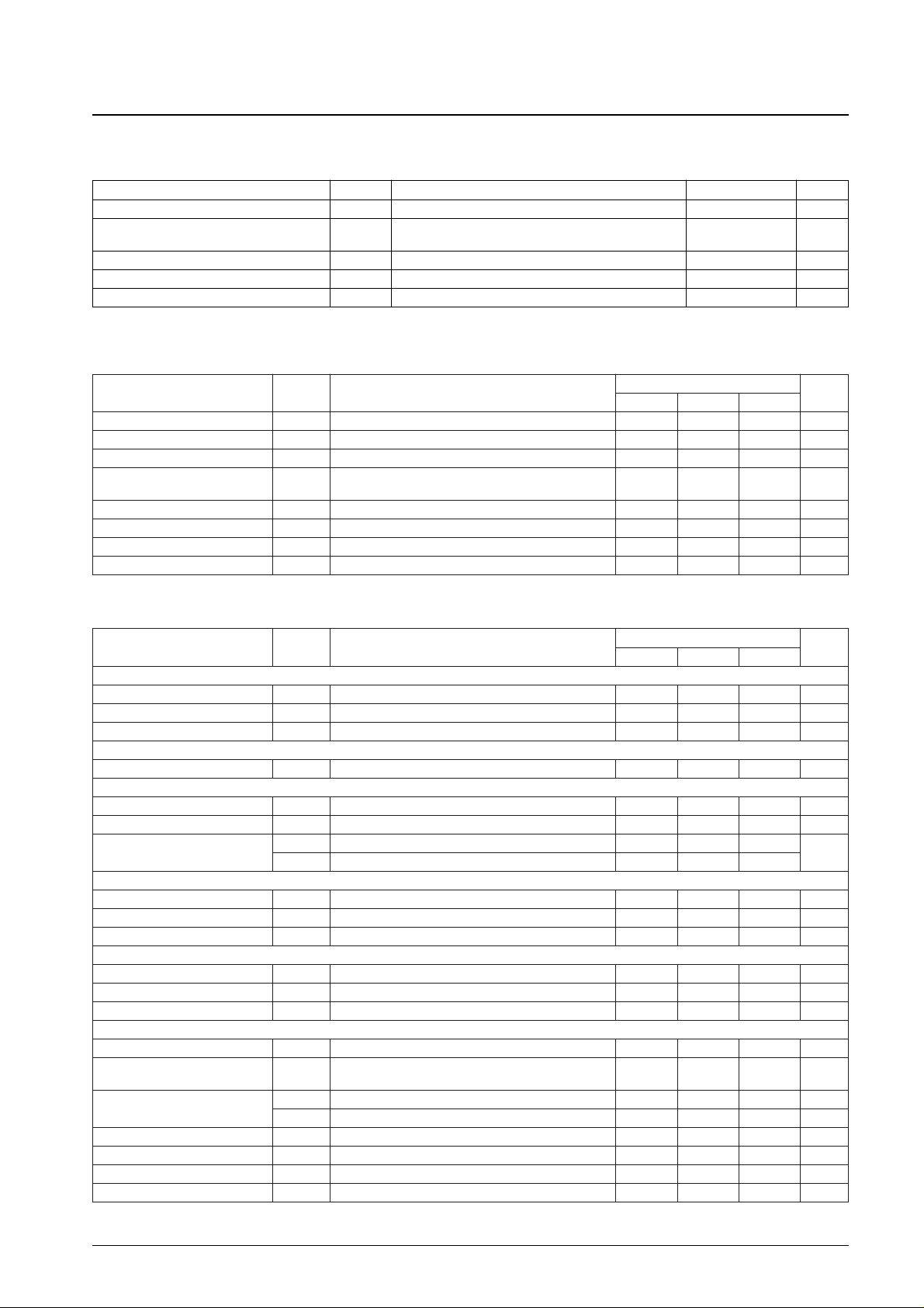
Pin Assignment
LC75397E
Top view
Page 4
No. 6108-4/26
LC75397E
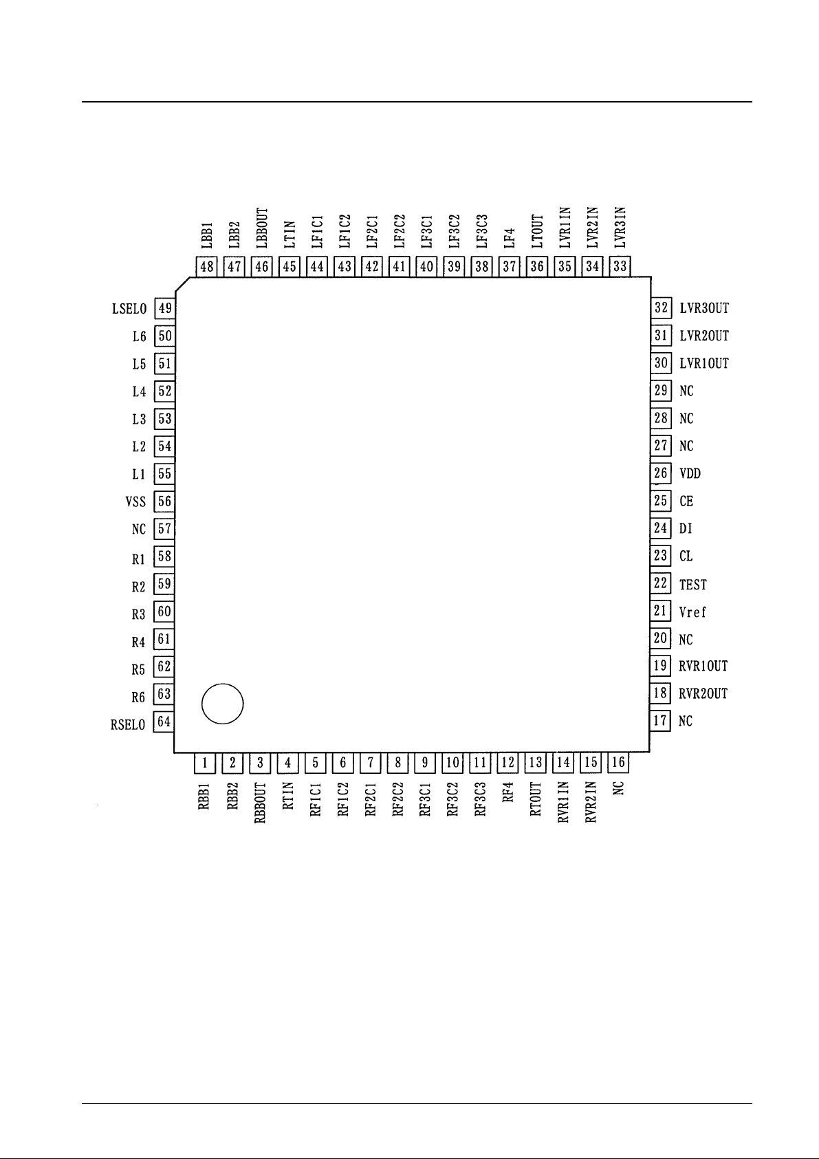
Sample Application Circuit
CCB
interface
Logic circuit
[f0 ≈ 39 Hz] [f0 ≈ 1984 Hz] [f0 ≈ 69 Hz] [fc ≈ 20000 Hz]
[f0 ≈ 39 Hz] [f0 ≈ 1984 Hz] [f0 ≈69 Hz] [fc ≈ 20000 Hz][f0 ≈ 148 Hz]
Control
circuit
LC75397E
[f0 ≈ 148 Hz]
Page 5
No. 6108-5/26
LC75397E
Control System Timing and Data Formats
To control the LC75397E, specified sequences are required to be input through the pins CE, CL, and DI. Each sequence
consists of 48 bits: an 8-bit address followed by 56 bits of data.
1. Address Code (B0 to A3)
This product uses an 8-bit address code, and supports the same specifications as other Sanyo CCB serial bus
products.
Address code (LSB)
2. Control Code Allocations
Input switching control
(L1, L2, L3, L4, L5,
R1, R2, R3, R4, R5)
Input switching control
(L6, R6)
D0 D1 D2 Operation
0 0 0 L1 (R1) ON
1 0 0 L2 (R2) ON
0 1 0 L3 (R3) ON
1 1 0 L4 (R4) ON
0 0 1 L5 (R5) OFF
1 0 1 Switch all OFF
0 1 1 Switch all OFF
1 1 1 Switch all OFF
D3 Operation
1 L6 (R6) OFF
0 L6 (R6) ON
1us ≤ T DEST
Page 6
No. 6108-6/26
LC75397E
Input gain control
D4 D5 D6 D7 Operation
0 0 0 0 0 dB
1 0 0 0 +2 dB
0 1 0 0 +4 dB
1 1 0 0 +6 dB
0 0 1 0 +8 dB
1 0 1 0 +10 dB
0 1 1 0 +12 dB
1 1 1 0 +14 dB
0 0 0 1 +16 dB
1 0 0 1 +18 dB
0 1 0 1 +20 dB
1 1 0 1 +22 dB
0 0 1 1 +24 dB
1 0 1 1 +26 dB
0 1 1 1 +28 dB
1 1 1 1 +30 dB
Bass and 4-band equalizer control
D8 D9 D10 D11 Bus
D12 D13 D14 D15 f1 band
D16 D17 D18 D19 f2 band
D20 D21 D22 D23 f3 band
D24 D25 D26 D27 f4 band
1 0 1 0 +10 dB
0 0 1 0 +8 dB
1 1 0 0 +6 dB
0 1 0 0 +4 dB
1 0 0 0 +2 dB
0 0 0 0 0 dB
1 0 0 1 –2 dB
0 1 0 1 –4 dB
1 1 0 1 –6 dB
0 0 1 1 –8 dB
1 0 1 1 –10 dB
Page 7
No. 6108-7/26
LC75397E
Volume control
D28 D29 D30 D31 D32 D33 D34 D35 Operation
0 0 0 0 0 0 0 0 0 dB
1 0 0 0 0 0 0 0 –1 dB
0 1 0 0 0 0 0 0 –2 dB
1 1 0 0 0 0 0 0 –3 dB
0 0 1 0 0 0 0 0 –4 dB
1 0 1 0 0 0 0 0 –5 dB
0 1 1 0 0 0 0 0 –6 dB
1 1 1 0 0 0 0 0 –7 dB
0 0 0 1 0 0 0 0 –8 dB
1 0 0 1 0 0 0 0 –9 dB
0 1 0 1 0 0 0 0 –10 dB
1 1 0 1 0 0 0 0 –11 dB
0 0 1 1 0 0 0 0 –12 dB
1 0 1 1 0 0 0 0 –13 dB
0 1 1 1 0 0 0 0 –14 dB
1 1 1 1 0 0 0 0 –15 dB
0 0 0 0 1 0 0 0 –16 dB
1 0 0 0 1 0 0 0 –17 dB
0 1 0 0 1 0 0 0 –18 dB
1 1 0 0 1 0 0 0 –19 dB
0 0 1 0 1 0 0 0 –20 dB
1 0 1 0 1 0 0 0 –21 dB
0 1 1 0 1 0 0 0 –22 dB
1 1 1 0 1 0 0 0 –23 dB
0 0 0 1 1 0 0 0 –24 dB
1 0 0 1 1 0 0 0 –25 dB
0 1 0 1 1 0 0 0 –26 dB
1 1 0 1 1 0 0 0 –27 dB
0 0 1 1 1 0 0 0 –28 dB
1 0 1 1 1 0 0 0 –29 dB
0 1 1 1 1 0 0 0 –30 dB
1 1 1 1 1 0 0 0 –31 dB
0 0 0 0 0 1 0 0 –32 dB
1 0 0 0 0 1 0 0 –33 dB
0 1 0 0 0 1 0 0 –34 dB
1 1 0 0 0 1 0 0 –35 dB
0 0 1 0 0 1 0 0 –36 dB
1 0 1 0 0 1 0 0 –37 dB
0 1 1 0 0 1 0 0 –38 dB
1 1 1 0 0 1 0 0 –39 dB
0 0 0 1 0 1 0 0 –40 dB
1 0 0 1 0 1 0 0 –41 dB
0 1 0 1 0 1 0 0 –42 dB
1 1 0 1 0 1 0 0 –43 dB
0 0 1 1 0 1 0 0 –44 dB
1 0 1 1 0 1 0 0 –45 dB
0 1 1 1 0 1 0 0 –46 dB
1 1 1 1 0 1 0 0 –47 dB
0 0 0 0 1 1 0 0 –48 dB
1 0 0 0 1 1 0 0 –49 dB
0 1 0 0 1 1 0 0 –50 dB
Continued on next page.
Page 8
No. 6108-8/26
LC75397E
D28 D29 D30 D31 D32 D33 D34 D35 Operation
1 1 0 0 1 1 0 0 –51 dB
0 0 1 0 1 1 0 0 –52 dB
1 0 1 0 1 1 0 0 –53 dB
0 1 1 0 1 1 0 0 –54 dB
1 1 1 0 1 1 0 0 –55 dB
0 0 0 1 1 1 0 0 –56 dB
1 0 0 1 1 1 0 0 –57 dB
0 1 0 1 1 1 0 0 –58 dB
1 1 0 1 1 1 0 0 –59 dB
0 0 1 1 1 1 0 0 –60 dB
1 0 1 1 1 1 0 0 –61 dB
0 1 1 1 1 1 0 0 –62 dB
1 1 1 1 1 1 0 0 –63 dB
0 0 0 0 0 0 1 0 –64 dB
1 0 0 0 0 0 1 0 –65 dB
0 1 0 0 0 0 1 0 –66 dB
1 1 0 0 0 0 1 0 –67 dB
0 0 1 0 0 0 1 0 –68 dB
1 0 1 0 0 0 1 0 –69 dB
0 1 1 0 0 0 1 0 –70 dB
1 1 1 0 0 0 1 0 –71 dB
0 0 0 1 0 0 1 0 –72 dB
1 0 0 1 0 0 1 0 –73 dB
0 1 0 1 0 0 1 0 –74 dB
1 1 0 1 0 0 1 0 –75 dB
0 0 1 1 0 0 1 0 –76 dB
1 0 1 1 0 0 1 0 –77 dB
0 1 1 1 0 0 1 0 –78 dB
1 1 1 1 0 0 1 0 –79 dB
0 0 0 0 1 0 1 0 –∞
Continued from preceding page.
Channel selection control
Volume 1 control
Right channel control is enabled when D36 is set to 1.
Left channel control is enabled when D37 is set to 1.
D36 D37 Operation
0 0 Initial setting
1 0 Righ channel
0 1 Left channel
1 1 Simulataneous left and right
D38 Operation
0 Control off
1 Control enabled
Volume 2 control
Right channel control is enabled when D36 is set to 1.
Left channel control is enabled when D37 is set to 1.
D39 Operation
0 Control off
1 Control enabled
Volume 3 control
Control of this function is enabled when D37 is set to 1.
D40 Operation
0 Control off
1 Control enabled
Test mode control
D41 D42 D43 D44 D45 D46 D47
0 0 0 0 0 0 0
These bits are for chip testing and must all be set to 0 in application systems.
Page 9

No. 6108-9/26
LC75397E
Pin Functions
Pin No. Pin Function Equivalent circuit
Signal inputs
55
54
53
52
51
50
58
59
60
61
62
63
L1
L2
L3
L4
L5
L6
R1
R2
R3
R4
R5
R6
Input selector outputs
49
64
LSELO
RSELO
Bass circuit inputs and outputs
48
47
1
2
46
3
LBB1
LBB2
RBB1
RBB2
LBBOUT
RBBOUT
Equalizer inputs
45
4
LTIN
RTIN
Connections for the resistors and capacitors that form the F1
band equalizer.
44
43
5
6
LF1C1
LF1C2
RF1C1
RF1C2
Connections for the resistors and capacitors that form the F2
band equalizer.
42
41
7
8
LF2C1
LF2C2
RF2C1
RF2C2
Continued on next page.
Page 10

No. 6108-10/26
LC75397E
Pin No. Pin Function Equivalent circuit
Connections for the capacitors that form the equqlizer F4
band filters
Connections for external capacitors
37
12
LF4
RF4
Connections for the resistors and capacitors that form the F3
band equalizer.
40
39
38
9
10
11
LF3C1
LF3C2
LF3C3
RF3C1
RF3C2
RF3C3
Connections for the resistors and capacitors that form the F3
band equalizer.
36
13
LTOUT
RTOUT
• Left channel volume input 1
• Left channel volume input 2
• Left channel volume input 3
• Right channel volume input 1
• Right channel volume input 2
35
34
33
14
15
LVR1IN
LVR2IN
LVR3IN
RVR1IN
RVR2IN
• Left channel volume output 3
• Left channel volume output 2
• Left channel volume output 1
• Right channel volume output 2
• Right channel volume output 1
32
31
30
18
19
LVR3OUT
LVR2OUT
LVR1OUT
RVR2OUT
RVR1OUT
Continued on next page.
Continued from preceding page.
Page 11

No. 6108-11/26
LC75397E
Continued from preceding page.
Pin No. Pin Function Equivalent circuit
• A capacitor with a value of a few tens of µF must be inserted
between Vref and AV
SS(VSS
) to reduce power supply ripple
in the 0.5 × V
DD
voltage generator block used for analog
ground.
21 Vref
• Chip enable
When this pin goes from high to low, data is written to an
internal latch and the analog switches operate. Data transfers
are enables when this pin is at the high level.
25 CE
• Electronic volume control test pin.
This pin must be held at the V
SS
potential.
22 TEST
• Unused pins. These pins must either be left open or
connected to V
SS
.
16
17
20
27
28
29
57
NC
• Serial data and clock inputs for chip control
24
23
DI
CL
Ground56
V
SS
Power supply26
V
DD
Page 12

No. 6108-12/26
LC75397E
Equivalent Circuit Diagram
(1) Selector Control Block
Right channel same as left
Unit (resistance : kΩ)
Page 13

(2) Bass control block internal equivalent circuit
No. 6108-13/26
LC75397E
The right channel is identical.
Units (resistance: kΩ)
Page 14

No. 6108-14/26
LC75397E
(4) F3/F4 band equalizer block internal equivalent circuit
(3) F1/F2 band equalizer block internal equivalent circuit
When providing boost, switches SW1 and SW3 are on, and when providing cut,
switches SW2 and SW4 are on. In 0-dB mode (through), the 0-dB switch and
switches SW2 and SW3 are on.
Right channel same as left
Unit (resistance: kΩ)
Right channel same as left
Unit (resistance: kΩ)
Page 15

Volume block internal equivalent circuit
No. 6108-15/26
LC75397E
Right channel same as left
Unit (resistance: kΩ)
Page 16

No. 6108-16/26
LC75397E
Test Circuits
Total Harmonic Distortion
The left channel is identical
Unit (capacitance : F)
Page 17

No. 6108-17/26
LC75397E
Output Noise Voltage
The left channel is identical
Unit (resistance : Ω, capacitance : F)
Page 18

No. 6108-18/26
LC75397E
Crosstalk
The left channel is identical
Unit (resistance : Ω, capacitance : F)
Page 19

External Capacitor Calculations
1. Bass circuit
The value of the external capacitor used by the LC75397E bass control can be calculated as shown in the example below.
Sample calculation: For a center frequency f0 of 39 Hz
Substitute the LC75397E internal resistors R1 and R2 shown below into the above formula.
This allows the value of the capacitor, C, to be calculated.
R1 = 1.3 kΩ
R2 = 57.993 kΩ
Assume C1 = C2 = C.
1
C = ——————
2πf0 R1R2
1
C = ——————————— ≠ 0.47 µF
2π × 39 × 1300 × 58000
Formula for calculating the gain:
R1 = 1.3 kΩ
R2U = 1.476 kΩ
R2L = 56.517 kΩ
R1 R1 (R2U + R2L)
G = (—————)2+ (—————————————)2= 3.16 = 10 dB
R1 + R2U (R1 + R2U) R1 (R2U + R2L)
Formula for calculating Q:
R1 (R2U + R2L)
Q = —————————————— ≠ G
(R1 + R2U) R1 (R2U + R2L)
No. 6108-19/26
LC75397E
Page 20

2. F1/F2 band circuits
This section presents the equivalent circuit and the formulas used to calculate the external resistor and capacitor values to
provide a center frequency of 148 Hz.
• F1/F2 band equivalent circuit
• Sample calculation
Specifications: Center frequency: f0 = 148 Hz
Gain at maximum boost: G
+10dB
= 10 dB
Assume R1 = 51.8 kΩ and C1 = C2 = C.
(1) Determine R2 from the specification that G
+10dB
= 10 dB.
R1
G
+10dB
= 20 × LOG101 + ——
2R2
R1 51800
R2 = ———————— = ——————— = 11979.7 ≠ 12 kΩ
2 (10
G+10dB/20
– 1) 2 × (3.162 – 1)
(2) Determine C from the specification that the center frequency f0 = 148 Hz.
1
f0 = ————————
2πf R1R2C1C2
1 1
C = —————— = ——————————— = 0.0431 × 10⁻⁶≠ 0.044 µF
2πf0 R1R2 2π × 148 51800 × 12000
(3) Determine Q.
C · C · R1 1 51800
Q = ————— · ————— = ———————— = 1.039
2C R1R2CC 2 51800 × 12000
No. 6108-20/26
LC75397E
()
Page 21

3. F3/F4 band circuits
The F3 band circuit supports peaking characteristics and the F4 band circuit supports shelving characteristics.
(1) Peaking characteristics (F3 band)
The external capacitor is used to construct a simulated inductor. This section presents the equivalent circuit and the
formulas for determining the desired center frequency.
(a) Simulated inductor equivalent circuit
(b) Sample calculation
Specifications: 1) Center frequency: f0 = 107 Hz
2) Q at maximum boost: Q
+10dB
= 0.8
(1) Determine the sharpness, Q0, of the simulated inductor itself.
Q0= (R1 + R4) / R1 × Q
+10dB
≈ 4.270
(2) Determine C1.
C1 = 1/2πf0R1Q0≈ 0.536 (µF)
(3) Determine C2.
C2 = Q0/ 2πf0R2 ≈ 0.021 (µF)
(c) Reference values for C1 and C2
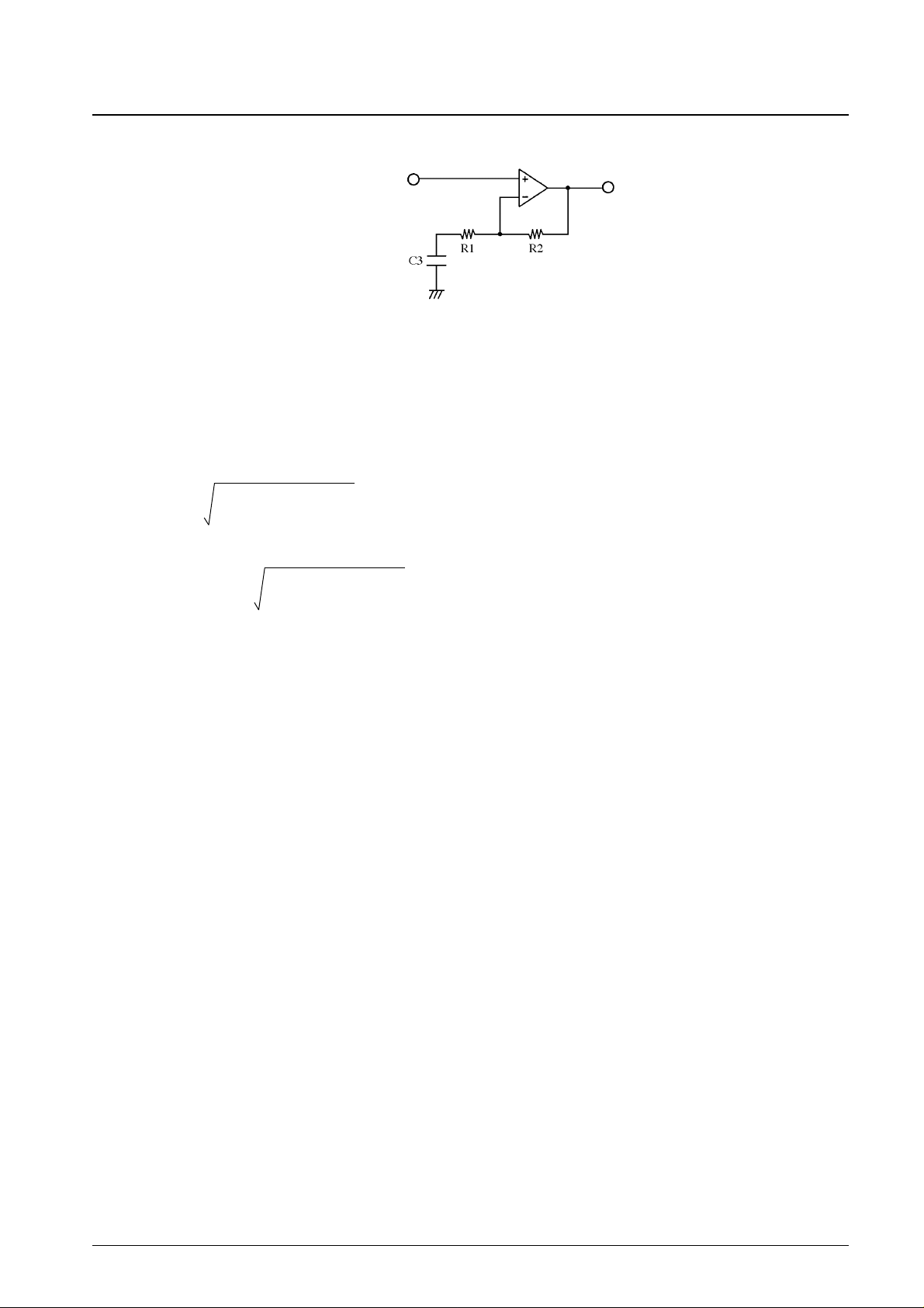
(2) Shelving characteristics (F4 band)
Gains of ±10 dB (in 2-dB steps) with respect to a target frequency can be achieved by using an external capacitor C3 with
a calculated according to the formula F shown below.
No. 6108-21/26
LC75397E
Z0: Impedance at resonance
(F3 band)
(F4 band)
Center frequency f0 (Hz) C1 (F) C2 (F)
107 0.536 µ 0.021 µ
340 0.169 µ 6663P
1070 0.054 µ 2117P
3400 0.017 µ 666P
Page 22
No. 6108-22/26
LC75397E
Sample calculation
Specifications: 1) Target frequency: f = 17,000 Hz
2) R1= 2,819 kΩ, R2 = 7.5 kΩ
1
C = ————————————
R2
2
2πf ————— – R1
2
10
G/20
– 1
1
= ——————————————
7500
2
2π × 17000 ———— – (2819)
2
3.16 – 1
≠ 4600 (pF)
()
()
Equivalent circuit and formula when boosting.
Page 23

No. 6108-23/26
LC75397E
V
DD
= +10 V
V
SS
= 0 V
V
IN
= 0 dBV
f = 1 kHz
Over all
Volume Step Characteristics
Step — dB
Volume attenuation — dBV
V
DD
= +10 V
V
SS
= 0 V
V
IN
= –20 dBV
External capacitance
C = 0.47 µF
Settings: +10 dB
to –10 dB, starting
at the top
Bass Band Frequency Characteristics
Frequency, f — Hz
Gain, G — dBV
V
DD
= +10 V
V
SS
= 0 V
V
IN
= –20 dBV
External C = 0.044 µF
External R = 12 kΩ
Settings: +10 dB
to –10 dB, starting
at the top
F1 Band Frequency Characteristics
Frequency, f — Hz
Gain, G — dBV
<Conditions>
V
DD
= +10 V
V
SS
= 0 V
V
IN
= –20 dBV
External C = 3200 pF
External R = 12 kΩ
Settings: +10 dB
to –10 dB, starting
at the top
F2 Band Frequency Characteristics
Frequency, f — Hz
Gain, G — dBV
Page 24

No. 6108-24/26
LC75397E
<Conditions>
V
DD
= +10 V
V
SS
= 0 V
V
IN
= –20 dBV
External C1 = 0.18 µF
External C2 = 0.15 µF
Settings: +10 dB
to –10 dB, starting
at the top
F3 Band Frequency Characteristics
Frequency, f — Hz
<Conditions>
V
DD
= +10 V
V
SS
= 0 V
V
IN
= –20 dBV
External C =
4700 pF
Settings: +10 dB
to –10 dB, starting
at the top
F4 Band Frequency Characteristics
Frequency, f — Hz
Gain, G — dBV
<Conditions>
V
DD
= +10 V
V
SS
= 0 V
V
IN
= 0 dBV
80 kHz low
pass weighting
Gain : 0 dB
Graphic
equalizer : flat
Volume : –10 dB position
Volume : 0 dB position
THD—Frequency Chapacteristics (1)
Frequency, f — Hz
Total harmonic distortion, THD — %
<Conditions>
V
DD
= +10 V
V
SS
= 0 V
V
IN
= 0 dBV
80 kHz low pass
weighting
Gain : 0 dB
Graphic
equalizer : flat
Volume : –10 dB position
Volume : 0 dB position
THD—Frequency Chapacteristics (2)
Frequency, f — Hz
Total harmonic distortion, THD — %
Gain, G — dBV
Page 25

No. 6108-25/26
LC75397E
<Conditions>
V
DD
= 0 V
V
IN
= 0 dBV
f = 1 kHz
80 kHz low pass
weighting
Gain : 0 dB
Graphic equalizer : flat
Volume : –10 dB position
Volume : 0 dB position
THD — Supply Voltage Characteristics (1)
Supply voltage, V
DD
— V
Total harmonic distortion, THD — %
<Conditions>
V
SS
= 0 V
V
IN
= –10 dBV
80 kHz low pass weighting
Gain : 0 dB
Graphic equalizer : flat
Volume : –10 dB position
Volume : 0 dB position
THD — Supply Voltage Characteristics (2)
Supply voltage, V
DD
— V
<Conditions>
V
DD
= 10 V
V
SS
= 0 V
80 kHz low pass weighting
Volume : 0 dB
position
Graphic equalizer : flat
f = 20 kHz
f = 1 kHz
THD — Input Level Characteristics (1)
Input level, V
IN
— dBV
Total harmonic distortion, THD — %
<Conditions>
V
DD
= 10 V
V
SS
= 0 V
80 kHz low pass weighting
Volume : –10 dB
position
Graphic equalizer : flat
THD — Input Level Characteristics (2)
Input level, V
IN
— dBV
Total harmonic distortion, THD — %
f = 20 kHz
f = 1 kHz
Page 26

PS No. 6108-26/26
LC75397E
This catalog provides information as of April, 1999. Specifications and information herein are subject to
change without notice.
Specifications of any and all SANYO products described or contained herein stipulate the performance,
characteristics, and functions of the described products in the independent state, and are not guarantees
of the performance, characteristics, and functions of the described products as mounted in the customer’s
products or equipment. To verify symptoms and states that cannot be evaluated in an independent device,
the customer should always evaluate and test devices mounted in the customer’s products or equipment.
SANYO Electric Co., Ltd. strives to supply high-quality high-reliability products. However, any and all
semiconductor products fail with some probability. It is possible that these probabilistic failures could
give rise to accidents or events that could endanger human lives, that could give rise to smoke or fire,
or that could cause damage to other property. When designing equipment, adopt safety measures so
that these kinds of accidents or events cannot occur. Such measures include but are not limited to protective
circuits and error prevention circuits for safe design, redundant design, and structural design.
In the event that any or all SANYO products (including technical data, services) described or contained
herein are controlled under any of applicable local export control laws and regulations, such products must
not be exported without obtaining the export license from the authorities concerned in accordance with the
above law.
No part of this publication may be reproduced or transmitted in any form or by any means, electronic or
mechanical, including photocopying and recording, or any information storage or retrieval system,
or otherwise, without the prior written permission of SANYO Electric Co., Ltd.
Any and all information described or contained herein are subject to change without notice due to
product/technology improvement, etc. When designing equipment, refer to the “Delivery Specification”
for the SANYO product that you intend to use.
Information (including circuit diagrams and circuit parameters) herein is for example only; it is not
guaranteed for volume production. SANYO believes information herein is accurate and reliable, but
no guarantees are made or implied regarding its use or any infringements of intellectual property rights
or other rights of third parties.
Usage Notes
• When the power is first applied, the internal analog switches are in indeterminate states. The chip therefore requires
muting or other external measures until it has received the proper data.
• After power is first applied, applications must initialize this chip by sending the initial data (1) and (2) described below.
• Provide grounding patterns or shielding for the lines to the CL, DI, and CE pins so as to prevent their high-frequency
digital signals from interfering with the operation of nearby analog circuits.
 Loading...