

Page 1
Overview
The LC7538JM is a fully equipped electronic volume IC
which permits significant reductions in externally
connected components while providing ample volume,
balance, loudness, fader, bass and treble control functions.
Features
• Volume : 81 positions ranging from 0 dB to -79
dB (in 1 dB increments) plus -∞.
Separate left and right control provides
excellent balance function.
• Loudness : Loudness operation provided by
externally attached CR to activate tap
at the -20 dB position of the volume
ladder resistor.
• Fader : Fader function traversing 16 positions
with rear or front attenuated output
only (these 16 positions consist of 2
dB step intervals ranging from 0 dB to
-20 dB, 5 dB step intervals ranging
from -20 dB to -45 dB, plus the end
settings of -60 dB and -∞).
•
Bass and Treble
: Using externally attached C
(capacitor), the LC7538JM provides
bass-treble mutual 15-position control
and formats a NF-form tone control
circuit (LUX form).
Ordering number : EN4799B
93098 HA (OT) / 83194 TH (OT) B8-0913 No. 4799-1/14
Specifications
Absolute Maximum Ratings at Ta = 25°C, VSS= 0 V
• On-chip op amplifier for caching applications reduces
external components.
• Reduced switching noise with silicon gate CMOS
processor.
• All controls performed using serial data input (CCB).
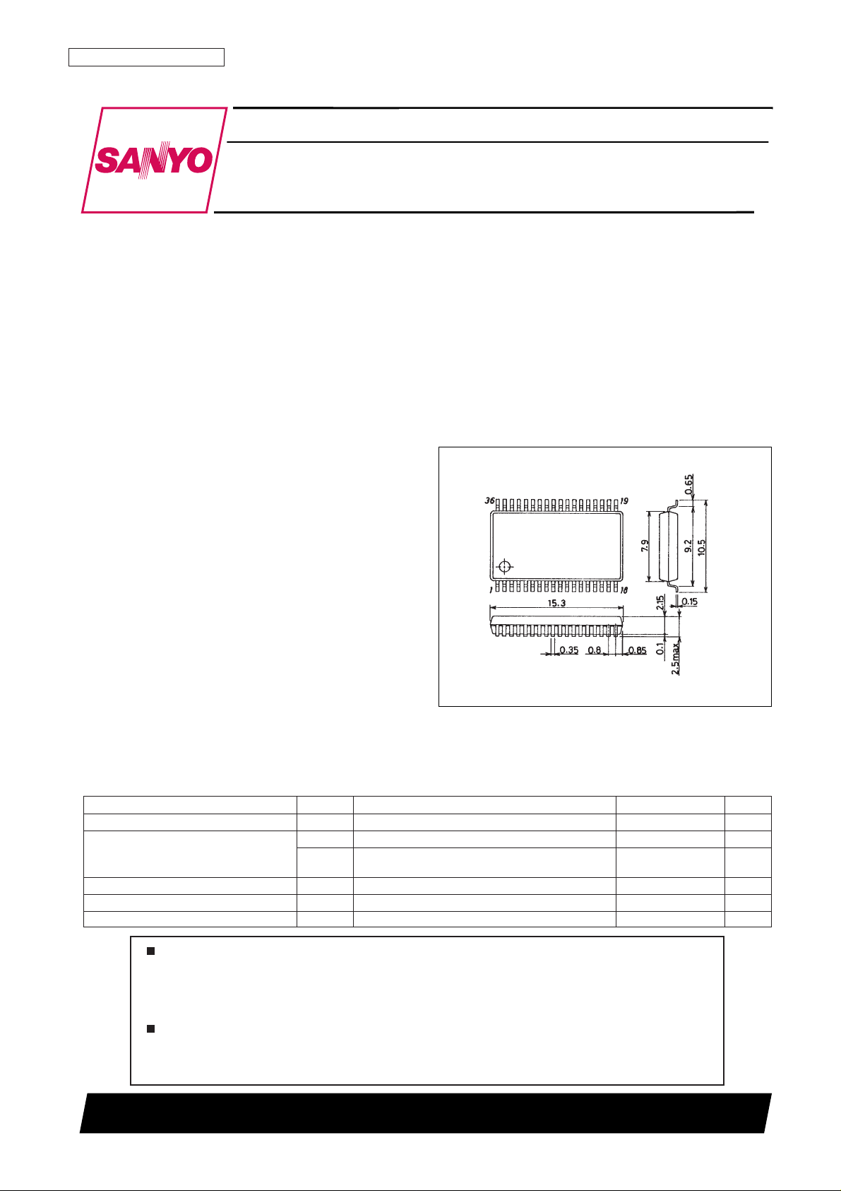
Package Dimensions
unit : mm
3204-MFP36S
Parameter Symbol Conditions Ratings Unit
Maximum supply voltage V
DD
max V
DD
11 V
V
IN
max1 CL, DI, CE VSS– 0.3 to V
DD
+ 0.3 V
Maximum input voltage
V
IN
max2
LTIN, RTIN, L5dBIN, R5dBIN, L1dBIN, R1dBIN,
VSS– 0.3 to VDD+ 0.3 V
LFIN, RFIN
Allowable power dissipation Pd max Ta ≤ 85°C 210 mW
Operating temperature Topr –40 to +85 °C
Storage temperature Tstg –50 to +125 °C
LC7538JM
Electronic Volume Control System
for Car Audio
CMOS IC
SANYO Electric Co.,Ltd. Semiconductor Bussiness Headquarters
TOKYO OFFICE Tokyo Bldg., 1-10, 1 Chome, Ueno, Taito-ku, TOKYO, 110-8534 JAPAN
Any and all SANYO products described or contained herein do not have specifications that can handle
applications that require extremely high levels of reliability, such as life-support systems, aircraft’s
control systems, or other applications whose failure can be reasonably expected to result in serious
physical and/or material damage. Consult with your SANYO representative nearest you before using
any SANYO products described or contained herein in such applications.
SANYO assumes no responsibility for equipment failures that result from using products at values that
exceed, even momentarily, rated values (such as maximum ratings, operating condition ranges, or other
parameters) listed in products specifications of any and all SANYO products described or contained
herein.
SANYO: MFP36S
[LC7538JM]
Page 2
LC7538JM
No. 4799-2/14
Allowable Operation Conditions at Ta = 25°C, VSS= 0 V
Note: 1. A capacitor rated at 2000 pF or less should be installed between all power supply pins and VSS.
Electrical Characteristics at Ta = 25°C, VDD= 9 V, VSS= 0 V
Parameter Symbol Conditions
Ratings
Unit
min typ max
Supply voltage V
DD
*1 7.0 10.0 V
Input high level voltage V
IH
CL, DI, CE 4.0 V
DD
V
Input low level voltage V
IL
CL, DI, CE V
SS
1.0 V
Input amplitude voltage V
IN
LTIN, RTIN, L5dBIN, R5dBIN, L1dBIN,
V
SS
V
DD
Vp-p
R1dBIN, LFIN, RFIN
Input pulse width t
øW
CL 1 µs
Setup time t
SETUP
CL, DI, CE 1 µs
Hold time t
HOLD
CL, DI, CE 1 µs
Operating Frequency fopg CL 500 kHz
Parameter Symbol Conditions
Ratings
Unit
min typ max
Total harmonic distortion
THD (1) V
IN
= 1 Vrms, f = 1 kHz, total overall flat 0.04 %
THD (2) V
IN
= 1 Vrms, f = 20 kHz, total overall flat 0.06 %
Crosstalk CT
V
IN
= 1 Vrms, f = 1 kHz,
60 87 dB
total overall flat, Rg = 1 kΩ
V
IN
= 1 Vrms, f = 1 kHz,
Maximum Output Reduction Vo min main volume –∞, fader volume –∞, 82 dB
C = 1000 µF between Vref and V
SS
for L/R
R
VOL
(1) 5 dB step 15 25 35 kΩ
R
VOL
(2) 1 dB step 12 20 28 kΩ
All Resistance Value R
FADER
12 20 28 kΩ
R
BASS
48 80 112 kΩ
R
TREBLE
30 50 70 kΩ
Input high level current I
IH
VI = 8 V (CL, CE, DI pins) 10 µA
Input low level current I
IL
VI = 0 V (CL, CE, DI pins) –10 µA
Output noise voltage V
N
All overall flat (IHF-A), Rg = 1 kΩ 7.5 15 µV
Current dissipation I
DD
VDD-VSS= 10 V 15 21 mA
CT1 1.8 3.0 4.2 kΩ
Between CT2 and Vref 0.6 1.0 1.4 kΩ
Analog switch on resistance R
ON
Fader S1 to S4 1.8 3.0 4.2 kΩ
–∞ 0.6 1.0 1.4 kΩ
All other cases 6.0 10.0 14.0 kΩ
Page 3
LC7538JM
No. 4799-3/14
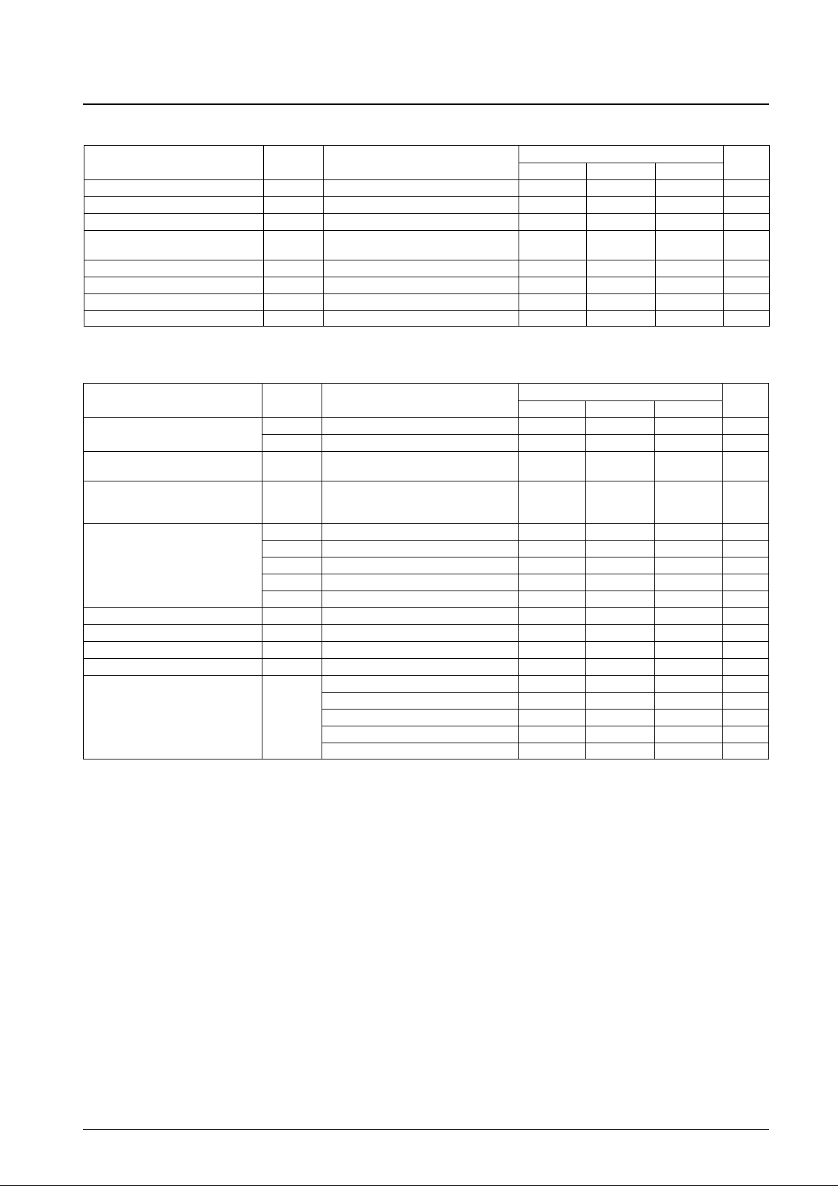
Equivalent Circuit Block Diagram
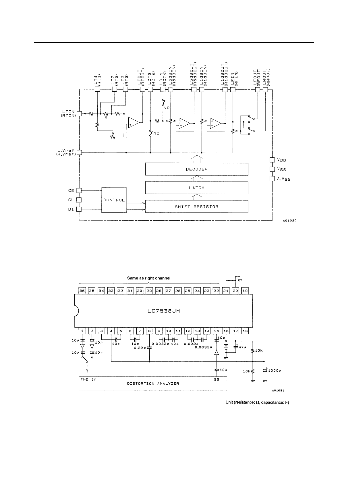
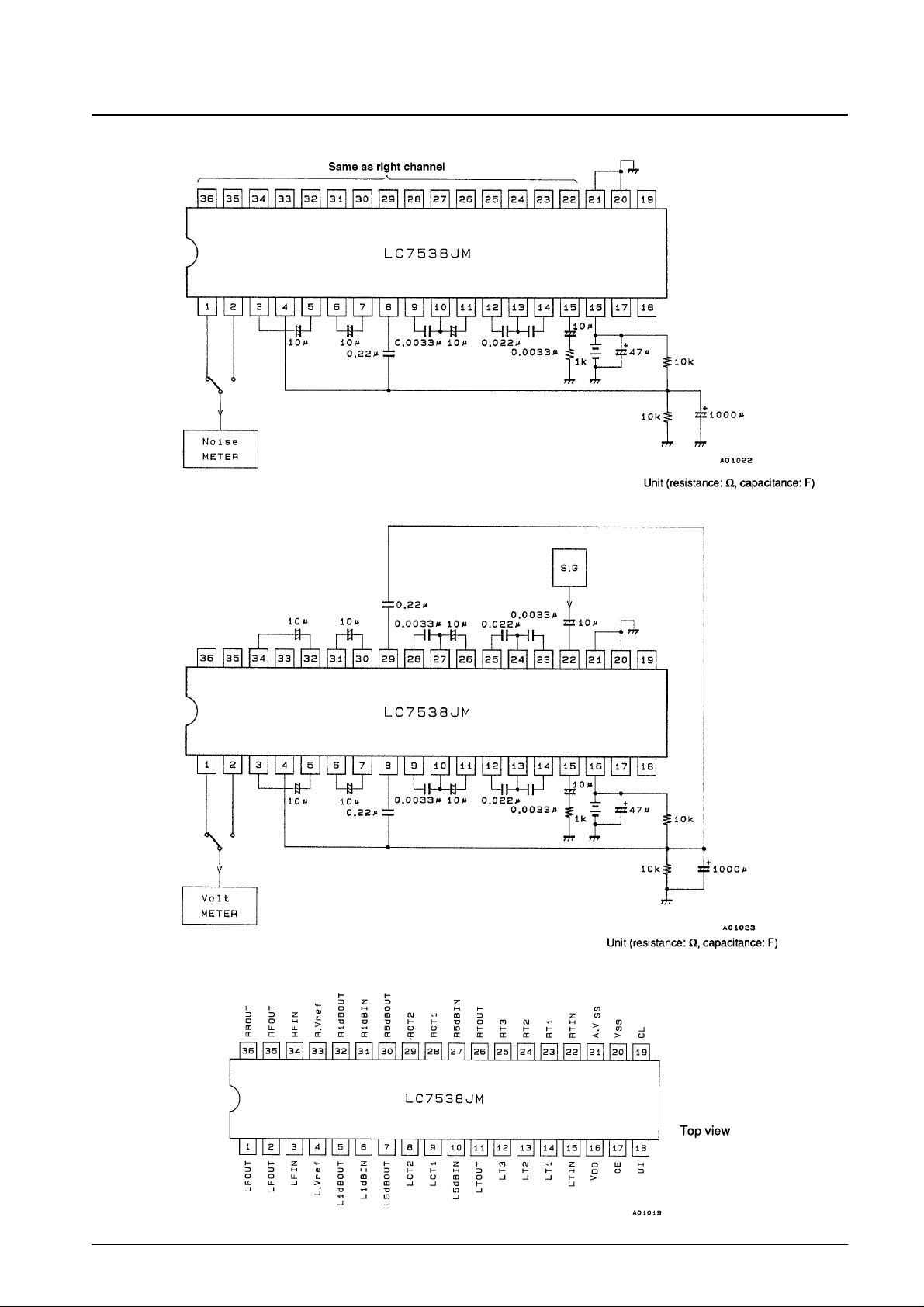
Test Circuit
a) Total Harmonic Distortion
Page 4
LC7538JM
No. 4799-4/14
b) Output Noise Voltage
c) Crosstalk
Pin Assignment
Page 5
LC7538JM
No. 4799-5/14
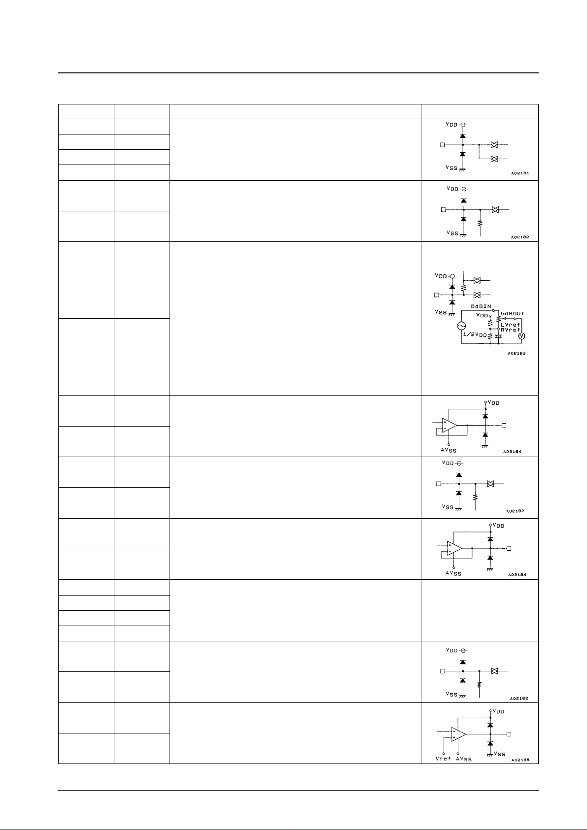
Pin Descriptions
Pin name Pin No. Description Remarks
LROUT 1
LFOUT 2
RROUT 36
RFOUT 35
LFIN 3
RFIN 34
LVref 4
RVref 33
L1dBOUT 5
R1dBOUT 32
L1dBIN 6
R1dBIN 31
L5dBOUT 7
R5dBOUT 30
LCT1 9
LCT2 8
RCT1 28
RCT2 29
L5dBIN 10
R5dBIN 27
LTOUT 11
RTOUT 26
•
These pins function as output pins for the fader. Output reduction for rear and
front is performed separately for each. Attenuation capacity is unified for
both left and right. Step positioning is designed using an open circuit so that
reception is performed using high impedance
.
• When utilizing the fader function, these pins function as input pins.
• Low impedance driven.
• These pins are common pins for fader volume, tone and main volume.
The pattern impedance connected here should be lowered as much as
possible.
• LVref and RVref are not connected to V
SS
.
• Connections for LVref and RVref to V
SS
should be established externally to
match all specifications. Notably, attention should be paid to capacity since
capacitors are subject to residual resistance during volume output reduction
when installed between LVref (RVref) and V
SS
as is the case with single
power sources.
• Normally, high voltage applied from VDD.
• These pins are output pins for the 1 dB step attenuator located in the section
main volume.
• These pins are input pins for the 1 dB step attenuator located in the section
main volume.
• Low impedance driven.
• These pins are output pins for the 5 dB step attenuator located in the section
main volume.
• These pins are for loudness control. Connect a high-band compensation
capacitor between CT1 to 5dB IN and a low-band compensation capacitor
between CT2 to Vref.
• These pins are input pins for the 5 dB step attenuator located in the section
main volume.
• Low impedance driven.
• These pins are output pins for tone control.
Continued on next page.
Page 6

LC7538JM
No. 4799-6/14
Continued from preceding page.
Pin name Pin No. Description Remarks
LT3 12
LT2 13
LT1 14
RT3 25
RT2 24
RT1 23
LTIN 15
RTIN 22
V
DD
16
A. V
SS
21
V
SS
20
CE 17
DI 18
CL 19
• These pins are for connecting bass and treble compensation for the tone
circuit.
Connect a high-band compensation capacitor between T1 and T2.
Connect a low-band compensation capacitor between T2 and T3.
• These pins are tone control input pins.
• Low impedance driven.
• Supply voltage pin.
• Ground pin for on-chip op amp.
• Ground pin for internal logic.
• This is the chip enable pin. According to the timing of the switch from high to
low, data is written to an internal latch and all analog switches operate.
Data transfer with high-level switches to enable.
• These are input pins for the clock and serial data for control.
Page 7

LC7538JM
No. 4799-7/14
Equivalent Circuit for Main Volume Section
Page 8

LC7538JM
No. 4799-8/14
Equivalent Circuit for Fader Volume Section
When data of -∞ is transferred to main volume
control 1 dB step, S1 and S2 open and S3, S4 are
turned on simultaneously.
Equivalent Circuit for Tone Section
Unit (resistance: Ω)
Page 9

LC7538JM
No. 4799-9/14
Control System Timing and Data Format
Controlling of LC7538JM involves the input of regulating serial data to CE, CL and DI pins. Data format consists of 36
bits composed of an 8-bit address and 28-bit data.
Page 10

LC7538JM
No. 4799-10/14
Sample Application Circuit
Same as right channel
Note: Bipolar electrolytic capacitors should be used as widely as possible where others are not recommended directly.
Page 11

LC7538JM
No. 4799-11/14
Page 12

LC7538JM
No. 4799-12/14
Page 13

LC7538JM
No. 4799-13/14
Loudness External Constant Calculation Sample
First, refer to page 7 where the 5 dB step internal equivalent circuit for the LC7538JM is shown. Using this information,
an external constant for loudness can be added to establish a simplified circuit for computation as shown in Figure 1.
Computations gaining a 5 dB boost with f = 100 Hz using this configuration are shown in the following.
(f = 100 Hz and 5 dB boost)
Within Figure 1, when R and C are defined as:
R1 = R2 = 10 kΩ
R3 = 1 kΩ
C1 =Z1, C2 = Z2, then the following equation can be established:
R2 (R3 + Z2)
R2 + R3 + Z2
V
OUT
= = –20dB
R1· Z1 +R2 (R3 + Z2)
(at = 1kHz)
R1 + Z1 R2 + R3 + Z2
R2 (R3 + 10 · Z2)
R2 + R3 + 10 · Z2
V
OUT
= = –15dB
R1 · 10 · Z1+R2(R3 + 10 · Z2)
(at = 100Hz)
R1 + 10 · Z1 R2 + R3 + 10 · Z2
thereby resulting in,
Z1 ≠ 178.3 kΩ and Z2 = 176 Ω.
Under such conditions where f = 1 kHz, specifications may be satisfied if C (capacitor) having these impedances is
supplied externally. The end result is that C1 = 893 pF and C2 = 0.9 µF.
R1, R2 and R3 : LC7538JM on-chip resistors
C1 : External high-band compensation capacitor
C2 : External low-band compensation capacitor
Figure 1
Notes for Above Applications
• When the power supply is turned on, the internal analog switch becomes inexact. Until data is set, counter measures
such as those required for muting are performed externally.
• In order to prevent crossover into the analog system of high-frequency digital signals transferred to the CL, DI and
CE pins, transfer along these signal lines should occur along shielded lines, or the signal lines should be protected by
using the grounding pattern or the circuit.
• Capacitors of at least 2000 pF must be inserted between each power supply pin and the VSSpin.
• For volume steps with large attenuation levels (over –20 dB), when the loudness circuit is off the high frequency
region (above about 4 kHz) will be attenuated by about 3 dB relative to the low frequency region (about 400 Hz) due
to the influence of the resistance of the loudness circuit analog switch. Therefore we recommend using tone control
compensation together with the volume step described above.
• When sending data immediately after power on, send data as follows:
— When sending independent left and right data, send data at least four times.
— Alternatively, when sending data that drives the left and right channels at the same time, send the data at least twice.
Page 14

LC7538JM
PS. No. 4799-14/14
This catalog provides information as of September, 1998. Specifications and information herein are
subject to change without notice.
Specifications of any and all SANYO products described or contained herein stipulate the performance,
characteristics, and functions of the described products in the independent state, and are not guarantees
of the performance, characteristics, and functions of the described products as mounted in the customer’s
products or equipment. To verify symptoms and states that cannot be evaluated in an independent device,
the customer should always evaluate and test devices mounted in the customer’s products or equipment.
SANYO Electric Co., Ltd. strives to supply high-quality high-reliability products. However, any and all
semiconductor products fail with some probability. It is possible that these probabilistic failures could
give rise to accidents or events that could endanger human lives, that could give rise to smoke or fire,
or that could cause damage to other property. When designing equipment, adopt safety measures so
that these kinds of accidents or events cannot occur. Such measures include but are not limited to protective
circuits and error prevention circuits for safe design, redundant design, and structural design.
In the event that any or all SANYO products (including technical data, services) described or contained
herein are controlled under any of applicable local export control laws and regulations, such products must
not be exported without obtaining the export license from the authorities concerned in accordance with the
above law.
No part of this publication may be reproduced or transmitted in any form or by any means, electronic or
mechanical, including photocopying and recording, or any information storage or retrieval system,
or otherwise, without the prior written permission of SANYO Electric Co., Ltd.
Any and all information described or contained herein are subject to change without notice due to
product/technology improvement, etc. When designing equipment, refer to the “Delivery Specification”
for the SANYO product that you intend to use.
Information (including circuit diagrams and circuit parameters) herein is for example only; it is not
guaranteed for volume production. SANYO believes information herein is accurate and reliable, but
no guarantees are made or implied regarding its use or any infringements of intellectual property rights
or other rights of third parties.
 Loading...